-
Paper Information
- Paper Submission
-
Journal Information
- About This Journal
- Editorial Board
- Current Issue
- Archive
- Author Guidelines
- Contact Us
Microelectronics and Solid State Electronics
p-ISSN: 2324-643X e-ISSN: 2324-6456
2016; 5(1): 14-18
doi:10.5923/j.msse.20160501.03

Fabrication and Analysis of Carbon Doped Hydrogenated Amorphous Silicon Thin Film Transistors
 Abstract
 Reference
 Full-Text PDF
 Full-text HTML
T. K. Subramanyam, Vinuth Nagendra, Goutham P., Pavan Kumar S., Subramanya K. N.
Interdisciplinary Research Centre, RV College of Engineering, Bengaluru, India
Correspondence to: Vinuth Nagendra, Interdisciplinary Research Centre, RV College of Engineering, Bengaluru, India.
| Email: |  |
Copyright © 2016 Scientific & Academic Publishing. All Rights Reserved.
This work is licensed under the Creative Commons Attribution International License (CC BY).
http://creativecommons.org/licenses/by/4.0/

Thin film transistors (TFT) are mainly used in display devices such as a LCD display or a LED display, as a current switch. This paper focuses on analysis of thin film transistors fabricated using carbon doped amorphous silicon as the semiconductor layer (a-Si:C:H). Radio Frequency Plasma Enhanced Chemical Vapour Deposition (RF-PECVD) technique was used to deposit the semiconductor active layer of a-Si:C: H as well as the dielectric silicon nitride layer. Thermal evaporation was used for depositing Aluminium as the gate, source and drain electrodes. Results from UV-VIS-NIR spectrophotometer suggests that the optimised semiconductor active layer with a thickness of 113 nm, exhibited a bandgap value of 1.88 eV. The TFT based on this a-Si:C:H showed linear I-V characteristics as measured using a semiconductor device analyser. Further a thin layer of diborone (B2H6) doped p type a-Si: H was added on top of the active layer (a-Si:C:H) and the TFT thus built showed diode characteristics at the Aluminium- p doped a-Si: H interface. It was thus learnt that using n–doped semiconductor layer with aluminium as the contact electrode provides better TFT characteristics than using Aluminium directly as the source drain material.
Keywords: a-SiC: H, RF-PECVD, Tauc Plot, TFT
Cite this paper: T. K. Subramanyam, Vinuth Nagendra, Goutham P., Pavan Kumar S., Subramanya K. N., Fabrication and Analysis of Carbon Doped Hydrogenated Amorphous Silicon Thin Film Transistors, Microelectronics and Solid State Electronics , Vol. 5 No. 1, 2016, pp. 14-18. doi: 10.5923/j.msse.20160501.03.
Article Outline
1. Introduction
- Thin film transistors (TFT) form a very important component in the displays such as LCDs and LEDs, where they are mainly used as switching elements that drive the current to the pixels. With the growing demand for flat panel displays, extensive research has been carried out in this field to find the optimum semiconductor active layer material, which can drive large currents, when incorporated in a TFT. As pointed out in [2], extensive research has been carried out on compound materials such as CdSe, to test their applicability in TFTs. However, they have not been introduced into the industry. Among all such materials researched, hydrogenated amorphous silicon (a-Si:H) was chosen as the semiconductor layer, which could be deposited using a Plasma Enhanced Chemical Vapour Deposition technique (PECVD) and has lesser process steps, making it easier to produce on large scale. However, a-Si:H TFTs have low charge mobilities (>1 cm2/Vs) [2]. Hence they can be used to drive current only to LCD pixels functioning at low frequencies and not OLEDs which generally need a larger drive current. This requirement prompted further research into TFTs and alternative materials such as poly-Si and organic semiconductors have been tested for the same. In poly-Si TFTs, the number of stages required to create poly-Si structures are more and alternative methods such as metal-induced crystallization and pulsed rapid thermal annealing have been used but they don’t possess uniform grain sizes. On the other hand, organic semiconductor thin films could be easily deposited using vacuum less technologies such as spin coating and hence can be looked up as cheaper alternatives for the conventional vacuum oriented thin film coatings. But these materials need very high gate driving voltages and are also unstable in air.A material such as SiC was also tested as the semiconductor material in TFTs in [1]. Accordingly, an amorphous layer of hydrogenated SiC (a-SiC: H) was first coated and then crystallized using KrF UV excimer laser annealing. The bandgap obtained for this material coating was between 1.9 -2.1 eV [1]. Use of SiC in a TFT has breakdown voltages as high as 2.4x10⁶ V/cm [4] and hence it will work efficiently even at very high applied electric fields. However the larger bandgap values of SiC will make the switching happen at relatively larger gate voltages.Considering all the above factors, TFTs made up of a-Si: H doped with small amounts of carbon were tested as the semiconductor material and its analysis is provided in this paper.The organization of the paper is as follows:1. Introduction2. Chemical composition and material analysis of SiC3. Structure of the Thin film transistor4. TFT Gate, Source and Drain material- Aluminium5. TFT dielectric material-Silicon Nitride6. TFT semiconductor material- a-Si:C:H7. Material Characterization8. Results9. Conclusion and future scope
2. Experimental
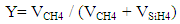
- a. Chemical composition and material analysis of a- Si:C:HPECVD was used to deposit a-Si:C: H layers, using Silane (SiH4), Methane (CH3) and Hydrogen (H2) as the precursor gases. Accordingly, the ratio of the gases used determines the composition of the coated material [3]. This is further substantiated in the parameter ‘Y’ equation [3].
 | (1) |
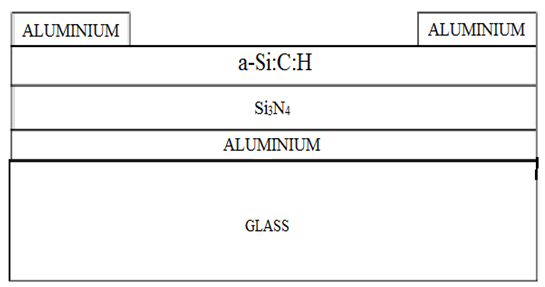 | Figure 1. Bottom gate TFT structure |
 | (2) |
3. Results
- The thickness of the optimised aluminium electrodes was around 300 nm thick with a contact resistance of 0.8 Ω. Similarly the Si3N4 thin films had a thickness of 400 nm and exhibited a band gap of 2.81 eV with a contact resistance of 2.94 GΩ. The a-Si:C:H semiconductor active layer has been optimized for a layer thickness of around 113 nm and a bandgap of 1.88 eV. Raman spectroscopy was carried out on the active layer samples to confirm the presence of Si-C bonding of a-Si:C:H. Fig. 2 shows the recorded Raman spectrum of the active layer which confirms the amorphous nature of the films and the peak obtained at 494 cm-1, confirms the presence of a-Si:C:H which clearly indicates the Raman shift from that of the pure a-Si:H at 481 cm-1 wave number.
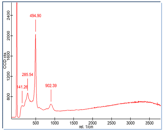 | Figure 2. Raman spectrum of a-Si:C:H |
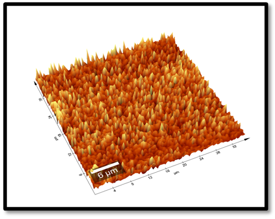 | Figure 3. Surface topology of a-Si:C:H as seen by an AFM |
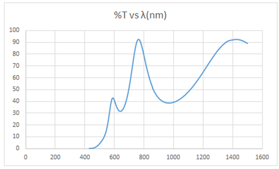 | Figure 4. Transmission curve for a-Si:C:H thin film |
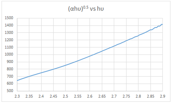 | Figure 5. Tauc plot for calculating bandgap of a-SiC: H |
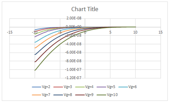
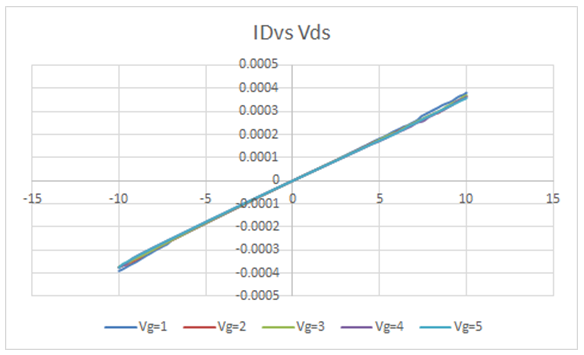 | Figure 6. Id vs Vds characteristics of a-Si:C: H TFT without an extra added layer of boron doped a-Si |
 | Figure 7. Id vs Vds characteristics of a-Si:C:H TFT with a small added layer of boron doped a-Si |
4. Conclusions and Future Scope
- a-Si:C: H is corrosion resistant, has relatively large band gap and also has good stability at high frequencies. Hence owing to its semiconductor nature, TFTs based on them were fabricated and analysed for a particular precursor gas ratio of SiH4, CH4 and H2. The presence of a-Si:C: H as an active layer was confirmed by Raman spectroscopy.The TFTs were fabricated on a glass substrate with bottom gate configuration. Oxygen plasma treatment was used to achieve good adhesion of the gate material aluminium on to the substrate. The electrical contact resistance of the obtained aluminium thin film was found to be 0.8 Ω. Suitable thickness of a-Si:C: H and Si3N4 dielectric were chosen and they were accordingly coated on the Gate material aluminium. Aluminium was again coated on top of these materials as the source and drain regions. In addition, TFTs were prepared by adding a thin layer of boron doped a-Si in between the semiconductor active layer and the source-drain regions. The band gap of the same material was calculated using a Tauc plot obtained from its transmission characteristics. The I-V characteristics of the two different TFTs were compared and it was found that: 1. With the lack of major charge carriers such as the holes and electrons, aluminium and a-SiC: H junction acts like a resistor with very high resistance and hence we obtain a linear graph as shown in Fig.6. The large thickness of Aluminium, helps in detecting any small change in current that passes through the transistor.2. It may be learnt from the experiment that the lack of depletion region in the Al- a-Si:C: H junction is due to the lower value of ‘Y’ selected for the PECVD growth of a-Si:C:H thin film.3. Upon addition of a thin layer of boron doped a-Si on the a-SiC thin film, the current ‘Ids’ increased with increasing gate voltage but the junction of aluminium and boron doped a-Si layer now shows diode characteristics (schottky contact) as shown in Fig.7. Boron doping, unlike in the previous step provides charge carriers but due to the schottky contact developed with the aluminium layer, all current that flows through is contact has an inherent rectifying action associated with it.4. To obtain good TFT characteristics, the source and drain regions could be a doped semiconductor thin film and aluminium can be used as their contact electrodes, instead of using aluminium directly as the source and drain regions.
ACKNOWLEDGEMENTS
- Authors are grateful to the Department of Science and Technology, New Delhi for the financial support through which the present work has been carried out.