-
Paper Information
- Previous Paper
- Paper Submission
-
Journal Information
- About This Journal
- Editorial Board
- Current Issue
- Archive
- Author Guidelines
- Contact Us
Microelectronics and Solid State Electronics
p-ISSN: 2324-643X e-ISSN: 2324-6456
2015; 4(1): 12-24
doi:10.5923/j.msse.20150401.03
Gate Stack High-κ Materials for Si-Based MOSFETs Past, Present, and Futures
 Abstract
 Reference
 Full-Text PDF
 Full-text HTML
Saeed Mohsenifar, M. H. Shahrokhabadi
Faculty of Electrical and Computer Engineering, Hakim Sabzevary University, Sabzevar, Iran
Correspondence to: Saeed Mohsenifar, Faculty of Electrical and Computer Engineering, Hakim Sabzevary University, Sabzevar, Iran.
| Email: |  |
Copyright © 2015 Scientific & Academic Publishing. All Rights Reserved.
An extensive discussion on the High-κ Metal Gate (HKMG) Stack for Si-based MOSFETs has been reviewed in this paper. The implementation of High-κ oxides is a developing strategy to allow more miniaturization of microelectronic components, for the sake of scaling down that predicted by Moore's Law. The main advantage of Silica (SiO2) as a traditional gate oxide is that it can be thermally grown conveniently on Si-substrate whereas its dielectric is an issue compared to the state of the art oxides. The term of High-κ oxide refers to a material with a high dielectric constant of κ, as compared to Silica, that candidate to replace Silica gate dielectrics in advanced CMOS applications. However, many issues such as electrical quality, thermodynamic stability, kinetic stability, gate compatibility and process compatibility remain to be resolved in the terms of implementation and process integration.
Keywords: High-κ Metal Gate (HKMG), MOSFET, High-κ oxides, Scaling down, Moore's Law, Silica, CMOS
Cite this paper: Saeed Mohsenifar, M. H. Shahrokhabadi, Gate Stack High-κ Materials for Si-Based MOSFETs Past, Present, and Futures, Microelectronics and Solid State Electronics , Vol. 4 No. 1, 2015, pp. 12-24. doi: 10.5923/j.msse.20150401.03.
Article Outline
1. Introduction
- Microelectronics has penetrated into our lives for the last sixty years. The simple multimedia experience that we have enjoyed from the first days of radio and TV right up to today’s world of the Internet that even a child can collect the information from it, would not have been possible without Microelectronics. The massive penetration of Microelectronics into consumer, communication and automotive markets mean that in 2014 a worldwide 82 billion USD investment in semiconductor materials and equipment led to 336 billion USD worth of semiconductor sales, which were built into 1,746 billion USD worth of electronics equipment as shown in Figure 1; so the Microelectronic is one of the main high technological knowledge and this property results high tech economy. So according to mentioned the cornerstone of high tech economy is semiconductor with its materials and equipment [1, 2].
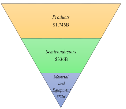 | Figure 1. Microelectronics world market for 2014 |
2. Scaling and Challenges
2.1. MOSFET Structure
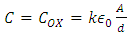
- The metal oxide field effect transistor (MOSFET) made from silicon is the main and fundamental electronic device among the any other devices such as Resistor and Capacitor devices, Diodes, Bipolar Junction Transistor (BJT), Thyristor, Metal–semiconductor field effect transistor (MESFET) and etc. It works as a solid state switch by applying a voltage across the source and drain as shown in Figure 2. As a voltage is applied to the gate electrode carriers are attracted to the surface of the Si channel and current can flow from the source to the drain where the current depends on the gate capacitance and is most simply expressed a:
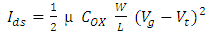 | (1) |
 | (2) |
 is the permittivity of free space, k is the relative dielectric constant, A is the area equal to L*W where L is the gate length, W is the channel width and d is the oxide thickness. The relative dielectric constant, κ, is defined according to Equation (3), where
  is the permittivity of the dielectric.
 | (3) |
 | Figure 2. Simple structure of MOSFET |
2.2. Scaling and Moore’s Law
- For decades, research and development of semiconductor processing technology and device integration have dedicated on improving performance and reducing costs using silica as the gate dielectric and doped polysilicon as the gate electrode. The most effective way to improve performance and reduce costs is to shrink or scale the device gate length and gate oxide as predicted by Moore’s Law.Moore’s Law motivated the economics of the semiconductor industry over the past half century, which is really the observation that as semiconductor manufacturing technology continually improves, the minimum manufacturing cost per device is continually decreasing and is realized by doubling the number of devices per unit area every two years. This very real trend first said by Gordon Moore in 1965, has continued steadily through nodes named in microns on to nanometer-scale nodes and very soon to nodes that one might expect will be termed in angstroms [2-5].The terminology of device nodes is the minimum feature size has arisen as a common way to reference each new technology as the minimum feature size in a transistor decreases exponentially each year (Figure 3). The device node at one time equated to the half-pitch or spacing between the tightest metal lines in Dynamic Random Access Memory (DRAM) chips, then migrated to become the minimum feature size in a given chip (typically Flash memory), and now the device node is effectively a marketing term that continues to decrease linearly even if no feature on the chip can be found to match it [2, 4].
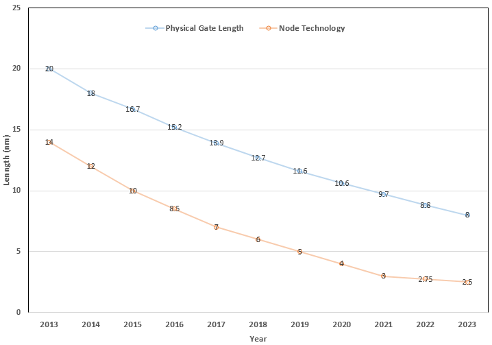 | Figure 3. The scaling of feature size and gate length according to the 2013 Semiconductor Roadmap [6] |
2.3. Problems Arisen from Shrinking
- This is probable that gate dielectric thickness will be the first parameter to reach atomic dimensions. This is because the dielectric thickness indirectly controls the gate length. In general, when the channel length becomes of the same order of magnitude as the depletion-layer widths of the source and drain, a MOSFET device is considered to be short and the so-called short-channel effects (SCE’s) arise. Thus, In order to continue scaling the planar MOSFET without harmful SCE’s, the effective gate length needs to be 40 times the dielectric thickness so the dielectric thickness must be decrease along with the physical dimensions of the device according to a general relation first proposed by Robert Dennard and his colleagues at IBM in 1974 [2, 3, 4, 8]. Dennard’s scaling rules were followed for decades on MOSFETs with Silica gate dielectrics to scaling with better performance.Despite succeeding Dennard’s scaling rules, by thinning of the gate oxide (Silica) beyond 20Å, uninvited gate leakage currents and gate oxide unreliability are perceived, so stand by power consumption and heat of the chips, which had originally been effectively constant, had arisen disturbingly [1, 9].The Silica layer used as the gate dielectric now is so thin (~1.2 nm) that produced at the 90 nm node; It is equal to only about four molecular layers of Silica and the gate leakage current due to direct tunneling phenomenon of electrons through the Silica becomes too high to continue scaling its physical thickness, exceeding 1A/cm2 at 1V (Figure 4). This means that the static power dissipation would be unsuitable [4, 5, 10]. In addition it becomes increasingly difficult to make such unreliable thin films. Thus at 65 nm the gate dielectric failed to scale, and it became necessary to introduce new materials as a dielectric at the 45 nm and below nodes [4].
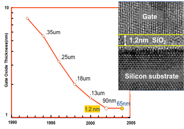 | Figure 4. 90nm node has a dielectric thickness of 1.2nm-Intel [11] |
2.4. Solution
- The solution to the tunneling problem is to replace Silica with a physically thicker layer of new material of higher k, as shown in transmission electron microscope images in Figure 5 [10, 12].
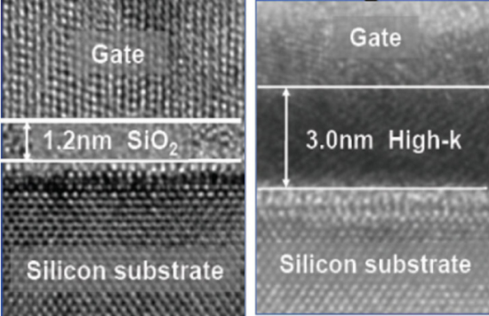 | Figure 5. TEM image of Silica based gate stack vs. image of High-κ gate stack [5] |
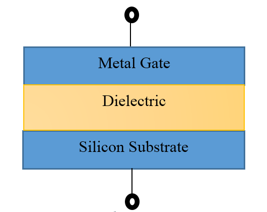 | Figure 6. A basic MOS capacitor |
 | (4) |
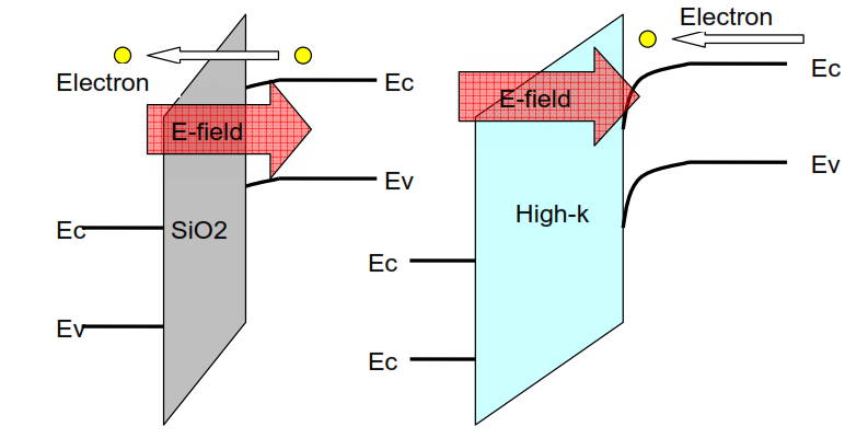 | Figure 7. Band diagrams of High-κ material and Silica [4] |
3. A Survey on High-κ Oxides
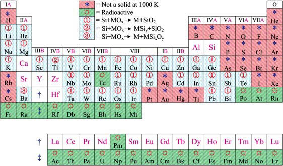
- Silicon is also used extensively as it is much more economical than other semiconductors but maybe the main reason that microelectronics uses Si technology is Silica. As a semiconductor, Si has average performance, but in most respects Silica is an excellent insulator. It has the key advantage that it can be made from Si simply by thermal oxidation, whereas every other semiconductor (Ge, GaAs, GaN, SiC . . .) has a poor native oxide or poor interface with its oxide. Silica is amorphous, has good quality of insulation, very few electronic defects and forms an excellent, abrupt interface with Si. It has the property of hard mask in different diffusion and doping process and can be etched or patterned to a nanometer scale. It has Chemical and thermal stability at high temperature and high breakdown fields of 13 MV/cm. So because of all above reasons Silica with the low k value of 3.9 has been used as the primary gate dielectric for over four decades since the tunneling occurred by scaling [5, 9].For CMOS application, High-κ oxides are defined as those with a relative dielectric constant greater than about 9 and refer to a class of simple binary and ternary metal oxide insulators, including transition metals from groups 3–5, the lanthanides and Aluminum [4].In the past ten years, significant development has been made on the screening and selection of High-κ oxides, understanding their physical properties, and their integration into CMOS technology. Among them are group IIIA metal oxides such as aluminum oxide (Al2O3), group IVB Metal Oxides and silicates such as titanium oxide (TiO2), zirconium oxide (ZrO2), zirconium silicate (ZrSiO4), Hafnium oxide (HfO2), hafnium silicate (HfSixOy), rare earth oxides, various lanthanides, and their silicates such as lanthanum oxide (La2O3), yttrium oxide (Y2O3), gadolinium oxide (Gd2O3), erbium oxide (Er2O3), neodymium oxide (Nd2O3), cerium oxide (CeO2), praseodymium oxide (Pr2O3), lanthanum aluminate (LaAlO3), tantalum oxide (Ta2O5), strontium titanate (SrTiO3), cerium zirconate (CeZrO4) and rare-earth scandates such as LaScO3, GdScO3, DyScO3 , and SmScO3 [3, 4, 9, 13].
4. Requisites for the Best Choice
- While the use of High-κ oxides sounds good in theory, many issues remain to be resolved in terms of implementation; e.g. the material must be compatible with the surrounding silicon and the fabrication processes that used. There are four key problems for successful introduction of High-κ oxides: (1) Be able to continue scaling to lower EOTs, (2) Stop the gate threshold voltage instabilities caused by the high defect densities (3) limit the loss of carrier mobility in the Si channel when using High-κ oxides (4) warrant reliability of the gate insulator. To do this, a material must be found that meets many criteria [1, 2, 5, 9].
4.1. Κ Value, Band Gap and Band Offset
- It is clearly essential that the first key requirement is the κ value. It must be high enough to use economically for a reasonable number of scaling nodes. The appropriate dielectric constant of the metal oxide should be over 12, rather 25–35. However, very large κ value will make unwanted strong fringing field from the gate to the source/drain regions. These fringing fields further induce electric fields from the source/drain to channel which declines the gate control and damages short-channel performances [9].
4.1.1. Band offset and Band Gap
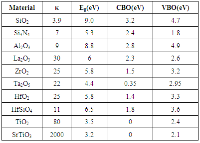
- The High-κ oxide must act as an insulator with a band gap larger than 5 eV, having the potential barrier at each band must be over 1eV as shown in Figure 8, in order to minimize the injection by the Schottky emission of carrier into the oxide bands that cause unacceptable high leakage currents. Also to prevent from the direct tunneling, it is necessary to find an insulator with a high κ value and high barrier to ensure low gate leakage current density. Table 1 lists the main dielectric materials with their κ and band gap (Eg) values as well as the conduction (valence) band offset, CBO (VBO). For example, the band gap of Silica is 9eV, so it has large barriers for both electrons and holes; the conduction and valence band offsets with Si are 3.1eV and 4.8eV, respectively. However, for oxides with a narrower band gap like SrTiO3, Ta2O5, TiO2 the CBO is very low and their bands must be aligned almost symmetrically with respect to those of Si for both barriers to be over 1eV. This limits the choice of oxide to those with band gaps over 5 eV. The oxides that satisfy this criterion are Al2O3, ZrO2, HfO2, Y2O3, La2O3 and various lanthanides, and their silicates and aluminates [5, 9].
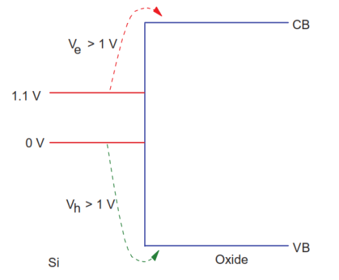 | Figure 8. Need for band offsets of over 1V in Si-Oxide |
|
4.1.2. Trade-off
- There is a trade-off between k value and the band offset, which requires a reasonably large band gap. Generally, the k-value of the High-κ dielectrics tends to vary inversely with their band gap, as shown in Figure 9; so we must accept a relatively low k value. For example, There are numerous ferroelectric oxides with extremely too high κ value, such as SrTiO3 (k = 200, Eg = 3.3 eV) unsuitable for MOSFET applications due to their rather small band gaps [9, 10].
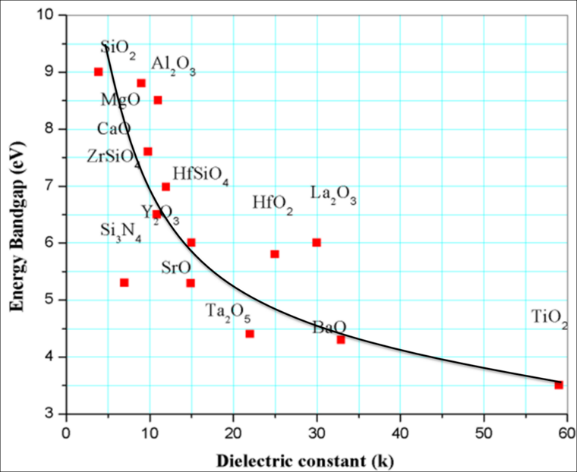 | Figure 9. Dielectric constant vs. band gap for candidate gate oxides [5] |
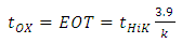
 , tunneling mass (m*) and dielectric constant (κ) and t is the EOT.
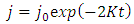 | (5) |
 | (6) |
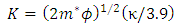
 | Figure 10. Leakage current density vs. EOT for various High-κ oxides [5] |
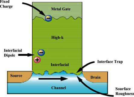
4.2. Interface Quality and Structural Defects
4.2.1. Electrically Active Defects
- Dielectrics must have few electrically active defects as a gate oxide. Electrically active defects are defined as atomic configurations which give rise to electronic states in the oxide band gap that can trap carriers. Normally, these are sites of extra or deficit of oxygen or impurities. They can be in the oxide or at the interface [1, 5]. Defects are unwanted because of:1. They cause unreliability; they are the starting point for electrical failure and oxide breakdown charges or high leakage current at best.2. Trapped charge scatters carriers in the channel and decreases the carrier mobility.3. Trapped charge in defects shift the gate threshold voltage of the transistor, Vth, the voltage at which it turns on. Also, the trapped charge changes with time too, so Vth shifts with time, leading to instability of operating characteristics.
4.2.2. Defects in High-κ Oxides
- The high electrical quality of the Si: SiO2 interface was the key advantage of Si as a semiconductor. There is a low concentration of defects in the Silica which give rise to states in the gap. The defects in Silica are primarily because of its low coordination number and dangling bond. The dangling bond can be removed by relaxing and re-bonding the network especially at the Si/SiO2 interface. Most of the remaining defects are readily passivized by hydrogen [5, 9].The electrical quality of the Si: High-κ interface also must be of the highest quality in terms of roughness and absence of defects in order to avoid scattering carriers. However, the High-κ oxides differ from Silica in that they are not basically low defect density materials; their bonding structure is ionic, and they have higher coordination number; so they have intrinsic defects such as oxygen vacancies, oxygen interstitials, or oxygen deficiency defects due to possible multiple valence of the metal. Among them, the large amount of oxygen vacancies is the primary source of oxide traps [5, 9]. In addition there is different processing between the metal oxides and conventional thermal oxide Silica; the electrically active defects can also be introduced into the High-κ oxide during the gate electrode deposition or Rapid Thermal Annealing (RTA) process due to high diffusivity of various species in High-κ oxides. These defects can be a source of fixed charges and electron traps, where the second may affect both the device performance and reliability [15].Therefore, the High-κ gate oxide has higher defect concentration than Silica; so much of the present engineering on High-κ oxides is trying to reduce defect densities by process control and annealing. For example Metal oxides are deposited on the silicon substrate instead of thermally grown like Silica. The intrinsic quality of the deposited film is poorer to thermally grown; so a post-deposition annealing (PDA) under dilute oxygen ambient is necessary to receive high performance devices [13, 16, 17, 18].
4.2.3. Channel Mobility Degradation
- The objective of device scaling is to create smaller, faster devices. High speed requires high source–drain current, which in turn depends on the carrier mobility. Carriers in the FET behave like a two-dimensional electron gas. The carrier density is determined by the vertical (gate) electric field which induces them. The carrier mobility in a 2D electron gas is found to depend in a ‘universal’ way on the gate field, according to a so-called ‘universal mobility model’ [5]. The individual scattering process VI add up in to a total scattering rate v:
 | (7) |
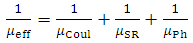 | (8) |
 | Figure 11. Factors contributing to carrier mobility degradation in a High-κ oxide layer [19] |
4.2.4. Reliability
- The reliability of the gate insulator has always been a main concern thru all CMOS generations. The High-κ dielectrics incline to show two important general reliability trends: (1) the breakdown strength is lower for the High-κ oxides versus Silica while (2) the local electric field is larger. Fortunately, most of the models and concepts that had been advanced for Silica or SiON reliability could be maintained on High-κ stacks. Similar to Silica, the High-κ oxides show some reliability phenomena including negative bias temperature instability (NBTI), positive bias temperature instability (PBTI), stress-induced leakage current (SILC), and time-dependent dielectric breakdown (TDDB) [9].The bias temperature instability was identified as one of the most limiting reliability issues in scaled CMOS technologies. It causes an increase in the threshold voltage and following decrease in drain current and transconductance of a MOSFET. The High-κ oxides such as Hf-based dielectrics present serious instabilities for negative and positive bias, after negative bias temperature and positive bias temperature stresses. NBTI is produced by two mechanism: the first is generation of new defects under the influence of the existence of holes at the High-κ/Si interface and the second is positive charge formation in the gate oxide. Whereas the PBTI only exists in the form of donor-like interface state generation that affects nMOS transistor when positively biased [20].Additional bulk traps in High-κ oxides are made during positive constant voltage stress, leading to dielectric breakdown when a critical trap density is reached that refers to TDDB. The breakdown is triggered by formation of a conducting path through the gate oxide to substrate due to electron tunneling current, when MOSFETs are operated close to or beyond their specified operating voltages. The generated traps give rise to SILC, which has to be taken into account in the actual process [21]. Again, defects are formed in the gate oxide at the Silica/Si interface due to flow of charge carriers. This may cause quasi-breakdown on the gate oxide layer [9].
4.3. Thermodynamic Stability on Silicon
- In MOS structure the gate oxide is in very close contact to the Si channel, so for all gate dielectrics, the interface reactivity with Si substrate is very important and, in most cases, is the dominant factor in defining the general electrical properties. Stability requires no or little reaction of the High-κ oxide with Si to prevent form either silica or a silicide layers by the reactions as described below [5, 6, 13].As mentioned in section 4.4.2 in the gate-first process the PDA is necessary, therefore the oxide must to be processed at the dopant activation anneal for 5 seconds at 1000◦C [1]. Most High-κ oxides, however, form a crystalline structure after a relatively high temperature annealing. Therefore the oxygen limited in the ambient of the PDA diffuses through the grain boundaries of the metal oxides and reacts with silicon substrate, which forms a Silica interlayer, so the Silica layer usually grows during the PDA stage, not during High-κ oxide growth [13, 16, 17, 18].
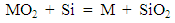 | (9) |
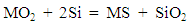 | (10) |
4.3.1. Interlayer
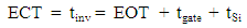
- An interlayer of silica or silicate usually exists between the Si channel and the High-κ oxide layer that degrade the properties of the dielectric and the underlying silicon or of both [22]. From an electrical perspective the silica interface layer and High-κ oxide layer can be treated as two capacitors connected in series and the overall EOT is given by the series capacitance formula:
 | (11) |
 | (12) |
4.3.2. Some Solutions
- The continued scaling of EOT below 1.0 nm and towards 0.5 nm requires us to either reduce the thickness of the silica interlayer, or increase the k values. Unluckily, many of the High-κ candidates are thermodynamically unstable at the interfaces with Si, as shown in Figure 12. Maybe a proper way to avoid reactions between a High-κ oxide and silicon is to select the oxides have a larger heat of formation (per O atom) than Silica. In other words we can use High-κ oxides with low oxygen diffusion coefficients to overcome this problem [5, 9]. There are very few oxides that pass this criteria.
 | Figure 12. Thermodynamic stability of binary oxides in contact with Si [9] |
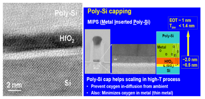 | Figure 13. (a) HRTEM cross section showing Silica interlayer below the HfO2 layer (b) Schematic of need for MIPS to minimize oxygen ingress |
4.4. Kinetic Stability
- The third condition is kinetic stability that is related to PDA in ‘gate first’ process [5, 9]. In first step we must choose to use a crystalline or amorphous oxide.
4.4.1. Polycrystalline and Amorphous
- The grain boundaries of crystallized gate dielectrics in thermal processes may behave as high leakage paths for the oxygen, dopant, and impurities diffuse fleetly in the polycrystalline; this might cause higher leakage currents and degrade the electrical properties of the gate stack; also the roughness of the film surface influence both the leakage current and reliability of High-κ oxide films [9, 13, 17, 18].Another potential concern is controlling the grain size among small devices and wafers, grain size and orientation changes throughout the film lead to fluctuating K values from grain to grain. So this may lead to the need for an amorphous interfacial layer to reduce leakage current.Amorphous metal oxides can easily be deposited, reduce O and dopant diffusion and lower defectively, so the oxides don’t suffer from grain boundaries; however, they usually have a lower dielectric constant than those metal oxides with a polycrystalline structure [13].
4.4.2. Crystallization Problem
- The most High-κ oxides usually have low crystalline temperature and can easily crystallize when subjected to RTA. In practice, HfO2, ZrO2, TiO2, and rare-earth oxides crystallize at lower temperatures would be nanocrystalline [1, 9, 17, 30]. However, it is preferable that gate insulators stay amorphous after a conventional activation annealing (800°C) because it is a concern that grain boundaries may serve as the paths of dopant diffusion and produce a variation of electrical properties. So it is desired to select another High-κ gate dielectric material that remains amorphous during the necessary processing treatments. However, Lee [31] and Kim [32] found that leakage currents of amorphous and nanocrystalline HfO2 are similar, so there was no specific conduction along grain boundaries.The crystallization problem can be solved by alloying the oxide with a glass former such as Silica or Al2O3, giving either a silicate or an aluminate [33, 34]. This holds a stability against crystallization up to nearly 1000°C. However, silicates have significantly smaller k values. Also the adding of nitrogen is very operative to reducing diffusion rates and increasing crystallization temperatures, so that Hf silicates can then pass this criterion [35].
5. Gate Compatibility
5.1. Metal Gate and Effective Capacitance Thickness
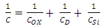
- Viewing the Si–gate stack band diagram of a MOSFET (Figure 14), the gate capacitance is the series combination of three terms, the oxide capacitance, the depletion capacitance of the gate electrode, and the capacitance of the Si channel carriers. These three capacitances add as:
 | (13) |
 | Figure 14. The three contributions to the capacitance of the gate/electrode stack; channel, dielectric and gate depletion [5] |
 | (14) |
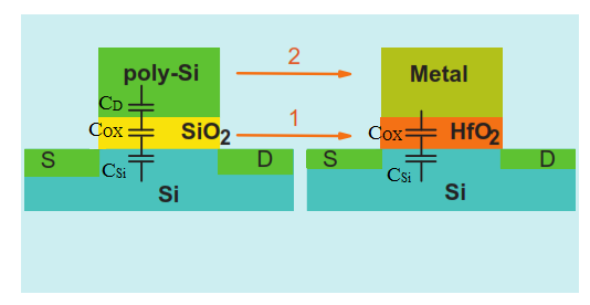 | Figure 15. Schematic of replacement of Silica gate oxide and the poly-Si gate by High-κ gate oxide and metal gate, showing effect on gate capacitances |
5.2. Threshold Voltage Control
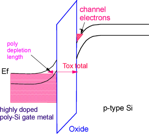
- Another key challenge with respect to the High-κ gate oxides system is threshold voltage (Vth) control [9]. Unlike Silica, High-κ oxide usually has large amounts of fixed charge [36]. The charge-trapping centers responsible for the fixed charge pose a serious issue for Vth control. But this is not the only reason, it has been found that Fermi-level pinning also plays an important character in Vth control in actual application of High-κ oxides. Fermi-level pinning occurs at the poly-Si/High-κ gate interface due to the defect formation through metal–Si bonding such as Hf–Si bonds [36, 37, 38, 39]. Calculation showed that the interaction between metal and Si atoms could produce surface dipoles at the poly-Si/High-κ interface that modify the interface barrier height and then the flat-band voltage (Vfb). It would result an unusable Effective Work Function (EWF) with asymmetric Vth shift (i.e., 0.3 V shift for n-MOSFETs and 0.9–1.0 V shift for p-MOSFETs) has been observed for all High-κ oxides when utilizing poly-Si gate electrodes, meaning the Vth cannot be set near enough to the mid-gap of Si to allow the CMOS architecture to function [4]. Moreover, replacing the poly-Si gate electrode by metal gate electrodes could be a possible solution to these issues. Metal electrode materials with work functions near the mid-gap may suffer less from this Fermi-level pinning effect. Another source of the instability in EWF could be diffusion of dopants (mostly boron). Adding a relatively small amount of nitrogen to the High-κ oxide is expected to suppress the boron diffusion through the dielectric, as has been generally effective with current SiOxNy applications [9].
5.3. Some Challenges with Metal Gates
- As noted above, scaling would ultimately needs the replacement of Silica by a High-κ oxide, and of the poly-Si gate by a metal gate, it was expected that the two technical changes could happen discretely. However, it became clear that there was a reaction between Si and High-κ oxide. Whereas the poly-Si gate electrode is compatible with Silica, the HfO2 atoms diffuse much more easily and reactions with metal gates arise at lower temperatures [5]. In instance, it was found that the reducing ambient during the CVD deposition poly-Si from silane makes a gross reduction of the High-κ oxides such as ZrO2 or HfO2, leading to silicide formation [37]. The interface between the gate metal and the gate oxide is at least as serious to the MOFET performance as that between channel and the oxide because this interface sets the Vth. So it was accepted that High-κ oxides and metal gates must be introduced at once with proper fabrication process. This led to the conclusion to develop a ‘gate last’ process against ‘gate first’ process.In addition, a metal gate material must be carefully chosen. It is chosen primarily for its work function and its thermal robustness. The work function of the metal is a critical property to enable suitable MOSFET operation [5].
6. Current and Future Applications
- The gate leakage problem has been obvious since the late 1990s, but the standards for choosing the new dielectric were unclear. In about 2001, the choice of oxide had limited to HfO2, but the problems of making HfO2 into a successful electronic material were great as mentioned in section 4. However, the increasing importance the low power electronics in cell-phones, lap-tops, and portable electronics mean that the problem had to be solved. Low standby power CMOS requires a leakage current of below 1.5
 10-2A/cm2 [5]. In order to continue device scaling to the 45 nm and below nodes, semiconductor device makers have implemented High-κ and Metal Gate (HKMG) stacks within the MOSFETs used in digital CMOS technology, which forms the basis for low power logic circuits within microprocessors and systems on a chip [40].In 2007 Intel became the first logic device maker to report Hf-based HKMG transistors in CMOS manufacturing. Since then, Hf-based HKMG technology has gained wide acceptance within the industry [6]. A basic planar bulk HKMG transistor, illustrated graphically in Figure 16, the gate dielectric included of a very thin silica interlayer and an Hf-based High-κ layer [4].
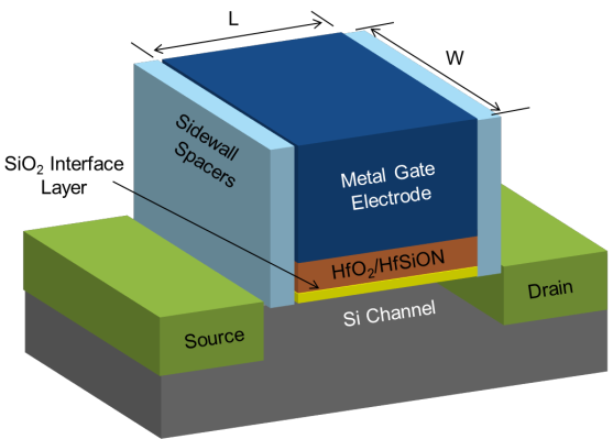 | Figure 16. Schematic diagram of a basic planar HKMG MOSFET [4] |
6.1. Incorporated Materials
- Most High-κ oxides result in an unusable EWF as mentioned in section 4.2. So, adjusting interlayer thickness for EOT minimization, while maintaining EWF control, mobility and reliability, has become the main effort for EOT scaling in Si based devices [4]. One potential alternative High-κ oxides which does not suffer from the problem with the EWF shift has recently seen renewed interest as well, namely ZrO2. ZrO2 is infinitely miscible with HfO2, and due to their well-known similarity, Zr and Hf tend to have analogous precursors that do not react with each other deleteriously during Atomic Layer Deposition (ALD). Thus it is possible to form mixed Hf-Zr oxides easily with any desirable ratio of Hf: Zr by ALD [43, 44]. Thus, doping ZrO2 into HfO2, or using pure ZrO2 is one potential way to increase the κ value of the High-κ oxide stack due to their crystallization form [45]. In addition gate stacks incorporating ZrO2 along with HfO2 exhibit improved reliability, mobility, and charge trapping [46, 47]. Also, since HfO2 films show poor thermal stability causing in a rise in leakage current after succeeding thermal processing, incorporation of Al into HfO2 films helps to improve the thermal stability [3]. So, one of the options to improve an Hf-based dielectric properties as a gate dielectric consists in adding another metal.
6.2. Rare Earth Oxides
- The rare earth oxides, various lanthanides, and their silicates are also be counted as potentially promising candidates, despite the fact that in some cases the permittivity increase is only moderate [48]. Rare earth scandates have also been introduced as High-κ candidates for next generation of HKMG stack; for example, LaScO3, TbScO3, and SmScO3 has been reported to have permittivity value above 37 in the regime below than 0.3nm thicknesses and optical band gap of 5 to 7eV, which is considerably higher than those of the constituent oxides, Gd2O3 and Sc2O3 [49].
6.3. ITRS
- Device parameters of next generation is provided in the International Technology Roadmap for Semiconductor (ITRS). In the 2014 version of the ITRS, the scaling of the MOSFETs is expected to the near-term (through 2020) when the channel length should be 10.6nm, also the High-κ oxides with EOT< 0.5nm and low leakage current are projected. So reduction of the EOT will continue to be a difficult challenge in the near term despite the introduction of HKMG. Integration of materials with higher κ value while limiting the fundamental increase in gate tunneling currents due to band-gap narrowing are also grand challenges to be faced in the near-term (through 2020) and long-term (2021 and beyond). The complete gate stack material systems need to be optimized together for best device characteristics (performance) and cost [6].
6.4. New Structures
- However, even with High-κ oxides it has not been possible to continue scaling planar bulk MOSFETs below the 20 nm node for leading edge device makers, primarily because the EOT of the gate dielectric cannot be scaled according to Dennard’s scaling rules. In fact, the era of improving transistor performance according to Dennard scaling has passed and device makers are now using new knobs beyond pure dimensional scaling to improve device performance. In order to make up for the lag in EOT scaling device makers have introduced strained Si technology at 90 nm and below nodes which improves the mobility of the transistor by straining the Si channel, and at the 22 nm node and below device makers are introducing fully depleted device architectures that have improved short-channel performances enough to allow the channel length to scale without scaling the dielectric EOT as shown in Figure 17 [4].
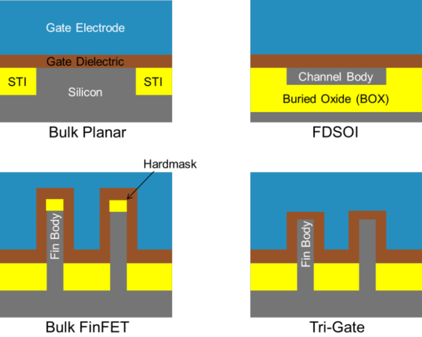 | Figure 17. Schematic cross-sections across the channel, looking from source to drain, of the transistor comparing traditional Bulk Planar with Fully Depleted Silicon on Insulator (FDSOI), Bulk FinFET and Tri-Gate device architectures which have been or will be implemented at the 22 nm and below device nodes [4] |
7. Conclusions
- Many different high-κ oxides have been proposed for replacing Silica as a MOS gate dielectric. Also, many challenges such as electrical quality, thermodynamic stability, kinetic stability, gate compatibility and process compatibility should be resolved in the terms of implementation and process integration. From these oxides and according to the challenges, HfO2 and HfO2-based materials emerges as a leading candidate to replace Silica gate dielectric in advanced CMOS applications due to some properties such as their compatibility with Si technology and high dielectric permittivity. In addition one of the way to enhance an Hf-based dielectric properties as gate dielectric consists in incorporating another metal such as Al. The rare earth oxides, various lanthanides, their silicates and recently rare earth scandates are also be counted as potentially promising candidates for MOS dielectric.According to ITRS, reduction of the EOT will continue to be a difficult challenge in the near term despite the introduction of HKMG. So new device architecture such as multiple-gate MOSFETs (e.g., FinFETs) and ultra-thin body FD-SOI are expected.