-
Paper Information
- Next Paper
- Paper Submission
-
Journal Information
- About This Journal
- Editorial Board
- Current Issue
- Archive
- Author Guidelines
- Contact Us
Microelectronics and Solid State Electronics
p-ISSN: 2324-643X e-ISSN: 2324-6456
2015; 4(1): 8-11
doi:10.5923/j.msse.20150401.02
KrF Excimer Laser Doping of Si into GaN
 Abstract
 Reference
 Full-Text PDF
 Full-text HTML
Essam Ali AL-Nuaimy
Department of Electrical Engineering, Zarqa University, Zarqa, Jordan
Correspondence to: Essam Ali AL-Nuaimy, Department of Electrical Engineering, Zarqa University, Zarqa, Jordan.
| Email: |  |
Copyright © 2015 Scientific & Academic Publishing. All Rights Reserved.
Silicon doping in undoped GaN has been performed by irradiating amorphous silicon film deposited by ion beam sputtering on GaN using 248 nm KrF excimer laser. Sheet resistances and depth profiles of the Si-doped GaN as functions of a number of laser pulses and laser fluence have been measured in order to clarify the relation between properties of doped GaN and irradiation conditions. The minimum sheet resistance of about 60 Ω / □ was obtained. SIMS analysis showed that Si is successfully diffused into GaN. The depths of doped regions ranging from 38 nm to 110 nm were obtained and can be readily controlled by irradiation conditions. Temperature-dependent Hall measurements for doped regions were investigated as a function of laser fluence.
Keywords: GaN, Capping layer, Excimer laser doping, Sheet resistance, Dopant profile, Hall measurements
Cite this paper: Essam Ali AL-Nuaimy, KrF Excimer Laser Doping of Si into GaN, Microelectronics and Solid State Electronics , Vol. 4 No. 1, 2015, pp. 8-11. doi: 10.5923/j.msse.20150401.02.
Article Outline
1. Introduction
- GaN as a wide band gap III-V compound semiconductor has been widely studied for applications in high-power and high electron mobility transistors (HEMT’s) [1-2]. High performance GaN HFET and MOSFET have been both demonstrated [3-5]. The GaN processing techniques are crucial in order to achieve good performance of GaN based devices. Most of the GaN devices are doped by ion implantation, which offers good uniformity and precise control of the dose as a function of depth and position on the substrate. However, implantation damage must be removed by a suitable annealing treatment to achieve better structural reordering and a high doping efficiency [6-8]. In production, ion implanted semiconductors have been annealed exclusively with furnaces or heat lamps. With these techniques, high temperatures are present over the entire sample, including the unimplanted layers, causing diffusion of atoms between layers. The laser doping method has been reported to produce superior device characteristics compared with other conventional doping methods. The short time duration (a few tens of nanosecond) of the ultraviolet excimer-laser pulse emitted makes it possible to confine the doped impurities to very shallow surface regions with extremely high dopant and high carrier concentrations [9-11]. By now a few published works devoted to the investigation of doping GaN substrate using an excimer laser to obtain conductive GaN [12-14]. In this paper, Si doping in undoped GaN with irradiation of 248 nm wavelength KrF excimer laser to melt amorphous silicon (a-Si) layer deposited on GaN is described. The variation of sheet resistance of doped GaN and depth profiles of silicon as functions of the laser fluences and the number of laser pulses will be discussed. Hall measurements suggested that the decrease of sheet resistance is due to the increase of charge carrier density.
2. Experiment
- Figure 1 shows the schematic cross-sectional view of the grown samples prepared for laser irradiation. First a 1.4 µm thick undoped GaN layer was grown by metalorganic chemical vapor deposition on 2 inch c-plane sapphire substrate. After this layer was grown, each sample was transferred via room ambient to ion sputtering chamber. A 60 nm amorphous silicon layer (a-Si) was deposited at room temperature, followed by 200 nm silicon dioxide (SiO2) as a capping layer to prevent amorphous silicon from blowing up during laser irradiation. Thermal diffusion effect makes the whole SiO2 capping layer to act as a heat capacitor and anti-reflection effect of the capping layer reduces the net light reflected from the sample [15]. Therefore the capping layer plays a role of heat capacitance for silicon melting and the diffusion of silicon into GaN during laser irradiation. The thicknesses for a-Si and SiO2 layer were optimized to allow laser radiation to fully melt a-Si and to be absorbed by GaN allowing the diffusion of Si-atoms into GaN. The propostion of the above multilayered structure was based on thermal calculations for the prediction of a melt threshold for the energy density of the laser [16].
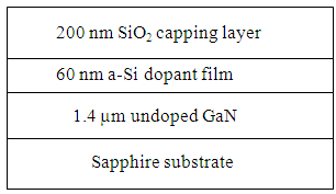 | Figure 1. Schematic structure of growing samples prepared for doping |
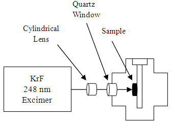 | Figure 2. Schematic diagram of the irradiation system for laser doping used in the present study |
3. Results
3.1. Sheet Resistance of Si Doped GaN
- Figure 3 shows the variations of sheet resistance as a function of the number of laser pulses at laser fluence of 650 mJ/cm2. It can be seen that increasing the number of pulses decreases the sheet resistance. Successive pulses add thermal energy to the surface and this should result in an increase of the lateral conduction of heat and hence the diffusion time so that more dopant can be incorporated into the GaN layer. Figure 4 shows sheet resistance versus laser fluence at 100 pulses. We see that increasing the pulse energy decreases the sheet resistance. It is believed that, as long as the dopant source has not been consumed, the higher the irradiation intensity the more dopant atoms can be incorporated into the GaN surface due to a larger melt depth [17], and because the time during which the layer is molten get longer, which could allow accommodation of more dopant atoms. The laser fluence was limited to 650 mJ/cm2 to avoid ablation of SiO2.
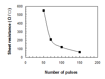 | Figure 3. The sheet resistance versus number of pulses for doped GaN layers made with laser fluence 650 (mJ/cm2) |
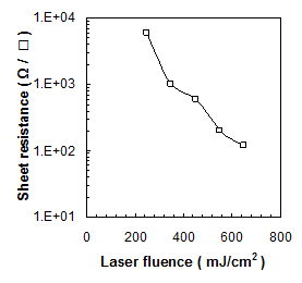 | Figure 4. Sheet resistance versus laser fluence for doped GaN layers fabricated with 100 pulses |
3.2. Dopant Depth Profile
- Si concentration and its depth profile for doped GaN layers were revealed by SIMS measurements. Figure 5 shows the concentration profiles of incorporating Si atoms for GaN layers made with 100 pulses at different laser fluences. The peak concentrations of Si were as high as (2-4) ×1020cm-3 at the surface for all samples. We see that increasing laser fluence causes Si-atoms to extend deeper, suggesting that doping depth is controlled easily by laser fluence. Increasing laser fluence increases the diffusion time and then allowing the Si atoms to diffuse deeper [18-19].
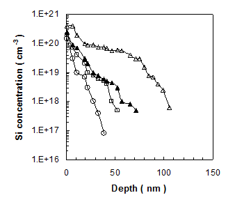 | Figure 5. Si concentration depth profile for doped GaN layers made at 100 pulses with different laser fluences: (Δ) 650 (mJ/cm2), (▲) 450 (mJ/cm2), (□) 350 (mJ/cm2), (○) 250 (mJ/cm2) |
3.3. Hall Measurements
- Hall measurements were used to determine the electron concentration with their ionization energy for Si-doped GaN layers. Figure 6 shows the carrier concentration (averaged over the whole thickness of the GaN layer) versus temperature for three samples made at 100 pulses with different laser fluences.
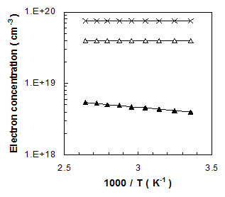 | Figure 6. Electron concentration as a function of inverse temperature for doped GaN layers made at 100 pulses with different laser fluences: (×) 650 (mJ/cm2), (Δ) 550 (mJ/cm2), (▲) 450 (mJ/cm2) |
4. Conclusions
- We have successfully demonstrated Si doping of GaN using a KrF excimer laser method. Dopant atoms were driven into the GaN from pre-deposited a-Si film during irradiation at atmospheric pressure. The laser irradiation causes the amorphous silicon to melt and to be diffused into GaN. Sheet resistance decreases with increasing laser fluence and the number of pulses. The minimum sheet resistance of 60 Ω/□ was obtained at 100 pulses with laser fluence 650 mJ/cm2. By changing the laser fluence and the number of pulses we can control the sheet resistance. SIMS analysis showed a depth of the doped region of about 105 nm. The average dopant concentration can be readily controlled by varying laser fluence. Hall measurements showed a maximum carrier concentration of about 7×1019 cm-3 with almost zero ionization energy obtained at 100 pulses with laser fluence 650 mJ/cm2. It has been shown that KrF excimer laser doping makes possible to fabricate highly conductive GaN layers. The process offers simplicity of operation without the need for sophisticated equipment.
ACKNOWLEDGEMENTS
- The author would like to acknowledge the financial support from Zarqa University.