-
Paper Information
- Paper Submission
-
Journal Information
- About This Journal
- Editorial Board
- Current Issue
- Archive
- Author Guidelines
- Contact Us
Microelectronics and Solid State Electronics
p-ISSN: 2324-643X e-ISSN: 2324-6456
2015; 4(1): 1-7
doi:10.5923/j.msse.20150401.01
Concurrent Dual-Band Power Amplifier Using Coupling Matching Network for 60 GHz WPAN Applications
 Abstract
 Reference
 Full-Text PDF
 Full-text HTML
Hanieh Aliakbari1, Abdolali Abdipour1, Rashid Mirzavand2
1Microwave/mm-Wave & Wireless Communication Research Lab, Radio Communication Center of Excellence, Electrical Engineering Department, Amirkabir University of Technology (Tehran Polytechnic), Tehran, Iran
2Intelligent Wireless Technology Lab, University of Alberta, Edmonton, Canada
Correspondence to: Hanieh Aliakbari, Microwave/mm-Wave & Wireless Communication Research Lab, Radio Communication Center of Excellence, Electrical Engineering Department, Amirkabir University of Technology (Tehran Polytechnic), Tehran, Iran.
| Email: |  |
Copyright © 2015 Scientific & Academic Publishing. All Rights Reserved.
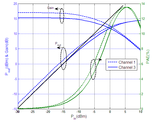
A new fully-integrated concurrent dual band CMOS power amplifier (PA) which covers the first and third channels of IEEE 802.15.3c standard is presented. In order to achieve concurrent operation of the 60 GHz PA in two desired narrow frequency bands, the multi-frequency passive coupling matching networks design is proposed. The full wave electromagnetic analysis (by the conventional Method of Moments (MOM)) and circuit analysis (using Circuit Envelope (CE)) are performed for the passive and active parts, respectively, in order to completely characterize the PA structure. This PA model has also been used in system level simulations. The results have shown two fractional bandwidths of 5% and 3%, P1dB of 8.8 dBm and 7.9 dBm at 58.32 and 62.64 GHz, respectively. Maximum power added efficiency (PAE) of 13% is achieved in both targeted bands. Performance of this PA shows promising availability in the future dual band WPAN applications.
Keywords: Dual band, Nonlinearity, Power amplifier (PA), 60 GHz
Cite this paper: Hanieh Aliakbari, Abdolali Abdipour, Rashid Mirzavand, Concurrent Dual-Band Power Amplifier Using Coupling Matching Network for 60 GHz WPAN Applications, Microelectronics and Solid State Electronics , Vol. 4 No. 1, 2015, pp. 1-7. doi: 10.5923/j.msse.20150401.01.
Article Outline
1. Introduction
- The federal communications commission (FCC) allocates 7 GHz frequency band from 57 GHz to 64 GHz for unlicensed use over the United States which covers the three channels of the IEEE 802.15.3c standard. In the context of high data rate wireless personal area networks (WPANs), which is the class of networks with a range below 10 m [1]; new consumer-oriented applications are emerging. Some radio frequency component design according to dual band scenarios have been suggested in 60 GHz frequency band. One of these dual band approaches is to operate the 60 GHz system in combination with a system that works at a lower [2] or higher frequencies [3]. Due to the minimum bandwidth requirement of about 2 GHz for 60GHz devices [1], allocation of two carrier channels using different classes for two WPAN high data rate arbitrary scenarios, in one transmitter architecture, is suggested. Our dual-band design, which is within 60 GHz band (Figure 1), is primarily motivated by future applications in indoor home and office networks.
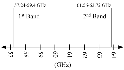 | Figure 1. Frequency band allocation |
2. 60 GHz Dual Band PA Design Method
- Figure 2 shows the block diagram of the proposed concurrent dual band 60 GHz PA. It consists of both passive and active sections. Two stage active portions have a role of providing power gain in the desired frequency band and passive portion provide matching and multi-band requirements, simultaneously. The design of the passive sections is based on input, inter stage and output matching networks which combine the conventional and coupling structures for providing dual band characteristic. Cascode topology is employed in active portion since it has better isolation and stability rather than common source stage [4]. Limited maximum available gain (MAG) is one of the problems of power amplifiers at 60 GHz which could be solved by choosing proper classes like A or AB. On the other hand, the transistor current density bias of about 0.3 mA/μm could help the transistor to operate in optimal linearity and peak fmax [5]. These considerations resulted in the single transistor bias at Vdd=1.2V and Vgs= 0.7V. The nonlinear transistor model used in this paper is based on 90nm CMOS BSIM which is modified to consider the high frequency parasitic effects of the device.
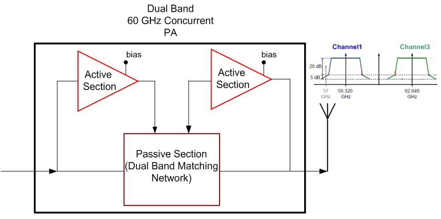 | Figure 2. Block diagram of the proposed concurrent dual band 60 GHz PA |
2.1. Output Stage
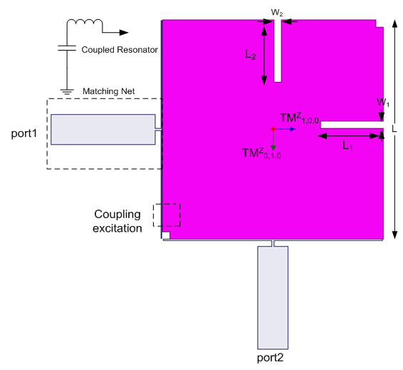
- The output matching network has a role of providing the optimum load for the second cascode stage in two desired frequency bands. In order to achieve the maximum output power in two desired bands finding optimum output impedance is essential. For this purpose the load pull simulation which is consisting of third order harmonic balance (HB) analysis (K=4), is employed for one stage cascode. Actually in this load pull simulation the passive losses have not been considered. Simulation results shows that due to the close middle channel frequencies optimum loading conditions for each band is almost similar (ZL1=21.49 +j21.49 Ohm and ZL2=16.76+j22.91 Ohm at the first and second bands, respectively). So the output matching network which consists of two series and parallel 50 Ohm lines and one structure for selecting two bands will be evident.Because of the small fractional bandwidth in each band (3%) coupling structure is utilized instead of conventional dual band matching network structures which are usually designed to achieve moderate-wide stop bands [16, 17]. By the idea of a coupled line structure, which is suitable for narrow band stop behavior, the output matching network can be optimized for realizing optimum load impedance in two frequency bands, simultaneously. The utilized structure is a half wave-length (λ/2) resonator edge-coupled to a 50 Ohm transmission line with a stepped-impedance distribution, as shown in Figure 3. The weak coupling between adjacent resonators at center provides flexible tuning of the narrow bandwidth. Stop-band behavior is obtained because of impedance mismatch over the middle frequency band. In order to improve the band stop behavior, four transmission zeros can be generated in middle band by cascading four unit-cells together. Furthermore, transmission zeros are created because of destructive interference of the signals propagating through the two paths and, as a result, sharp rejection characteristics are obtained.To prevent currents from injecting into the substrate and, hence, reduce the transmission loss, a ground plane is placed above the Si substrate. Ground plane is placed at the bottom metal (M1) to prevent external loss of close proximity of the ground plane to the signal line.Full wave simulation results show four transmission zeros in 59.63, 60.23, 60.68, 61.25 GHz frequencies. The final results will be demonstrated in section 2.3.
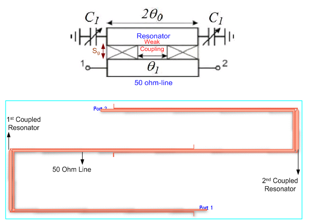 | Figure 3. Half wave-length (λ/2) resonators edge coupled to a through 50 Ohm line utilizing in an output stage |
2.2. Input Stage
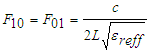
- In order to match the power amplifier to an input 50 Ohms and increase the power gain, an input stage is added to the power amplifier structure. Furthermore to keep away the interferences and isolate out band signals, adequate selectivity of about 7 GHz is needed for 60 GHz power amplifiers. From this point of view, matching to the 50 Ohm and narrow band pass filtering (~0.12) will be the defined role for input matching network.In the same way as output matching network, the coupling structure is utilized in an input matching network. In order to provide better performance the simple square patch on M7 layer is considered as a resonator due to the advantage of lower insertion loss in narrowband operation and higher power handling capability in comparison with line based resonators [18], which is in high importance in millimeter wave region. As illustrated in Figure 4 coupling to and from the resonator is facilitated by capacitive microstrip gaps. The axes of coupling to the resonator are orthogonal, so each couples energy independently to and from only one of the two orthogonal modes. Coupling to the resonator can be tuned for achieving narrowband operation of about 10%. By cutting away the corner geometry of the patch resonator two degenerate modes will be coupled. The initial dimension of the square patch will be:
 | (1) |
 | Figure 4. Example of an image with acceptable resolution |
 | (2) |
2.3. Final Circuit (Harmonic Balance and Small Signal Characterization)
- In this work, the proposed dual band matching network design technique was applied to the two stage power amplifier. Due to the parasitics in 60 GHz achieving a higher maximum output power by increasing the transistor width is not accessible (Figure 5). Therefore, by considering the technology limitations, the width and number of fingers in the output stage transistors have been fixed at Wg=3μm and Nf2=32, respectively. In order to have a better PAE, the number of fingers in the input stage transistors have been selected as Nf1=26.
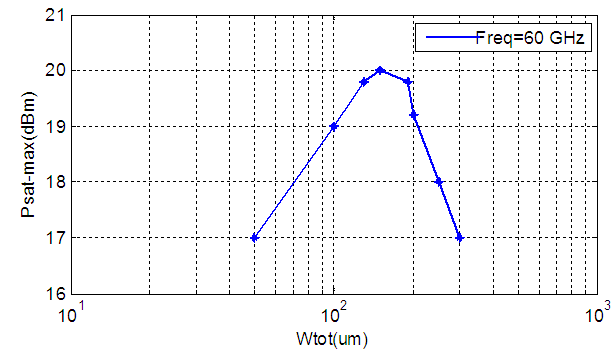 | Figure 5. Output power versus transistor width obtained by load pull simulations |
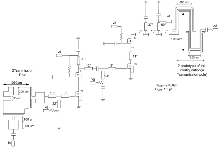 | Figure 6. Concurrent dual band PA structure |
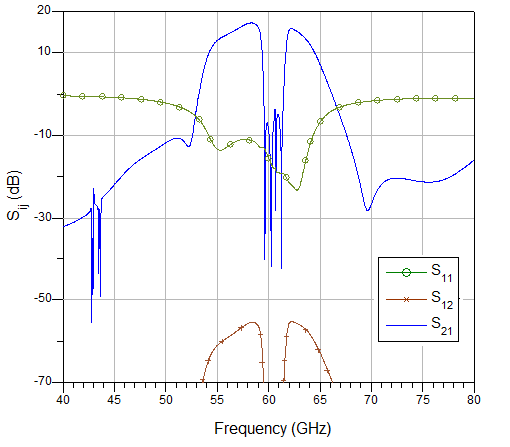 | Figure 7. The simulated scattering parameters of the dual band PA |
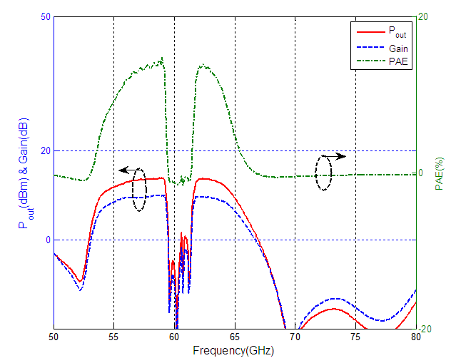 | Figure 8. The simulated behavior of the nonlinear figure of merits (FOMs) versus frequency at 4dBm input power |
 | Figure 9. FOMs as a function of frequency in two bands |
3. Single Carrier Characterization
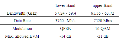
- As indicated in IEEE 802.15.3c standard draft [1], a total of three Physical layers (PHYs) are defined for the mmWave PHY. They are as follows:a) Single Carrier mode (SC PHY)b) High Speed Interface mode (HIS PHY)c) Audio/Visual mode (AV PHY)The HSI PHY and AV PHY (HRP, LRP) modes use orthogonal frequency domain multiplexing (OFDM). OFDM systems have higher peak-to-average power ratio (PAPR) than single carrier (SC) systems, thus power amplifier (PA) back off required to keep signal distortions due to PA non-linearity below the maximum allowed level in SC systems are typically lower, which results in higher PAE [19]. This section presents results of the PA non-linearity investigation for SC system in dual band 60 GHz WPAN scenarios. The single carrier mode in mm wave PHY (SC PHY) provides three classes of modulation and coding schemes (MCSs) targeting different wireless connectivity applications which occupy at least one channel bandwidth (~1.88 GHz) [1]. In this work the second and third SC class which support more than 1.5 Gb/s data rate has been used for driving 60 GHz power amplifier in each of the desired bands, respectively. This evaluation can be used for various data rate, dual band WPAN applications. A summary of SC systems parameters and requirement used in this work for PA non-linearity impact analyses are given in Table 1.
|
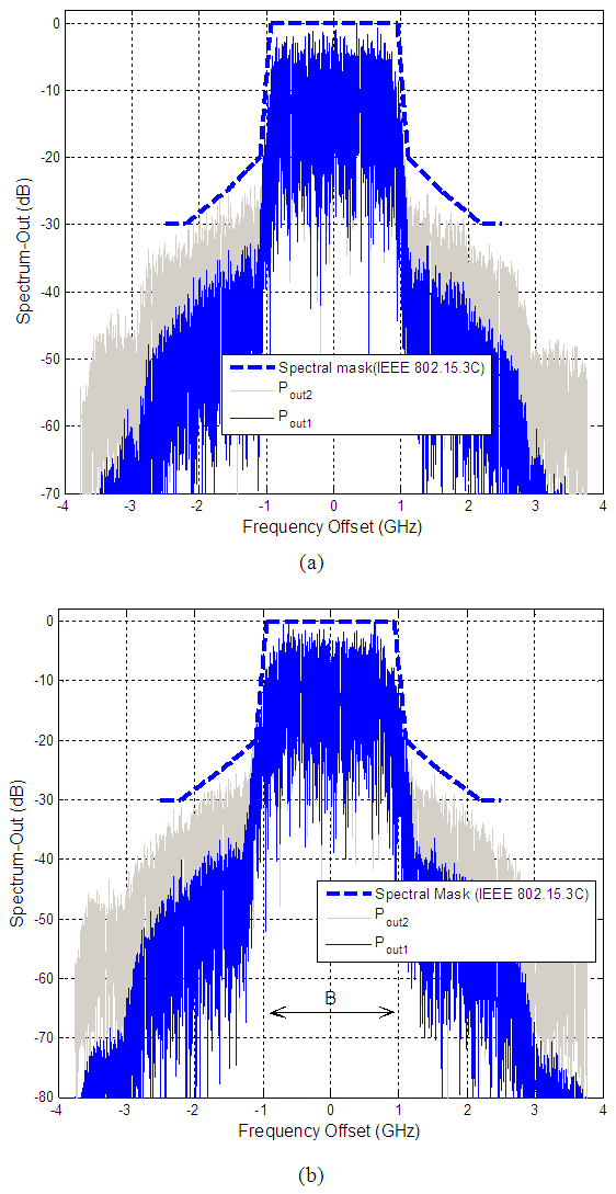 | Figure 10. Spectral regrowth phenomenon (Pout2>Pout1) in (a) first and (b) second band |
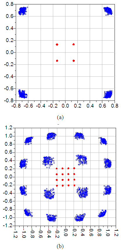 | Figure 11. The constellation diagrams of (a) QPSK signal in first band under 4dB OBO, (b) 16-QAM signal in second band under 3.8dB OBO |
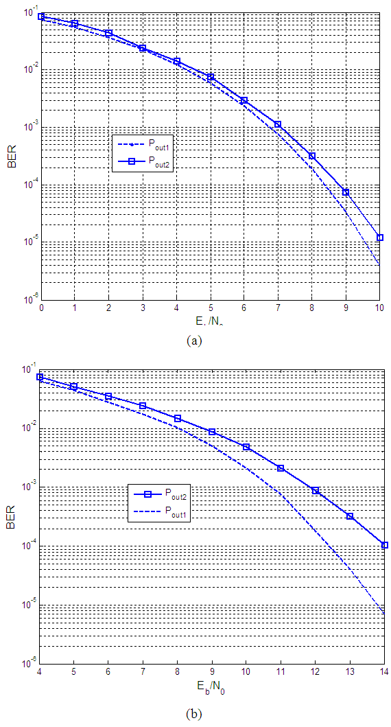 | Figure 12. BER results of two different Pout level in the (a) first and (b) second band |
4. Conclusions
- In this paper, design and analysis of a 60 GHz two-stage dual band PA is presented. For the realization of narrowband operation in both bands the dual band coupling structure in matching networks was utilized. Standard 90 nm-CMOS process was used for the analysis and design of the PA operating concurrently at the first and third channels in the IEEE 802.15.3c standard definition. The small signal and single carrier (SC) characterization of a dual-band 60 GHz PA based on IEEE 802.15.3c standard was described. The PA modeling is benefited from full wave electromagnetic and circuit analysis simultaneously in circuit and system level simulations. Two bands were evaluated by different standard modulated signals for various data rates dual band WPAN applications, in the future. It is believed that this is the first time proposing 60 GHz dual band PA structure which works concurrently at the first and third standard channels.
ACKNOWLEDGEMENTS
- The authors would like to thank Iran Telecommunication Research Center (ITRC) for supporting this work.