-
Paper Information
- Paper Submission
-
Journal Information
- About This Journal
- Editorial Board
- Current Issue
- Archive
- Author Guidelines
- Contact Us
Microelectronics and Solid State Electronics
p-ISSN: 2324-643X e-ISSN: 2324-6456
2014; 3(1): 11-14
doi:10.5923/j.msse.20140301.02
Effect of Metal-Semiconductor Contact Geometry on Electrical Properties of Al/ZnSe Thin Films
 Abstract
 Reference
 Full-Text PDF
 Full-text HTML
I. A. Amatalo1, N. E. Makori1, J. Maera2, D. Wamwangi3, P. M. Karimi1
1Department of Physics, Kenyatta University, Nairobi, Kenya
2Department of Physics, Maasai Mara University, Narok, Kenya
3School of Physics, University of Witwatersrand, Johannesburg, South Africa
Correspondence to: I. A. Amatalo, Department of Physics, Kenyatta University, Nairobi, Kenya.
| Email: |  |
Copyright © 2014 Scientific & Academic Publishing. All Rights Reserved.
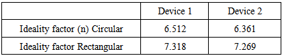
The desire for smaller, more efficient and faster semiconductor devices has made design of metal-semiconductor contacts and characterization very vital. There is little research if any on the effect of metal-semiconductor contact geometry on I-V characteristics of ZnSe thin films. Various circular and rectangular thin filmed Al/ZnSe devices were designed by varying the shape and area of the Aluminium metal contact. Fabrication was done by thermal vacuum evaporation technique of zinc (99.99%) and selenium (99.99%) alloy powder onto masked glass slides using an Edward Auto 306 RF/DC magnetron evaporation chamber. Aluminium metal was subsequently deposited on the ZnSe thin films using circular and rectangular masks. Silver paste was used as the ohmic contacts. I-V characteristics were obtained using the Keithley 2400 source meter and data analyzed using Origin Software. From the J-V characteristic curves, the dark diode ideality factors ranged between 6.0 and 7.3 and were lower for circular Schottky devices than for rectangular ones. Device with circular Schottky contact area of 2.0423×10⁻⁴m2; a smaller inter-electrode spacing of 4mm had the lowest diode ideality factor of 6.361.
Keywords: Metal- semiconductor devices, Schottky contact area, Vacuum deposition, Ideality factor
Cite this paper: I. A. Amatalo, N. E. Makori, J. Maera, D. Wamwangi, P. M. Karimi, Effect of Metal-Semiconductor Contact Geometry on Electrical Properties of Al/ZnSe Thin Films, Microelectronics and Solid State Electronics , Vol. 3 No. 1, 2014, pp. 11-14. doi: 10.5923/j.msse.20140301.02.
Article Outline
1. Introduction
- Zinc Selenide is a naturally n-type semiconductor with a cubic zinc blende structure and a direct band gap of 2.7eV at room temperature. Thin film Schottky devices provide a solution for cheaper, fast switching devices which can be incorporated with other thin film semiconductors to form thin film high speed optical devices, diodes or transistors among others [1]. There is limited research and literature if any on circular thin film Al/ZnSe Schottky diodes with top annular Aluminium Schottky contact and Silver as top Ohmic contact. Most literature is on rectangular Schottky contacts and preferably interdigitated contacts [2]. There is need to fabricate more efficient devices by taking into account the electric field and thus adjusting the geometry and area of Schottky contacts. The evaluation of a Schottky contact using diode ideality factor provides a useful method for characterizing metal-semiconductor devices. In this paper we report the effect of metal-semiconductor contact geometry on I-V characteristics.
2. Experimental
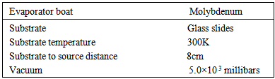
- Thin film depositions were carried out using an Edward Auto 306 RF/DC magnetron evaporation chamber and the deposition parameters are presented in table 1. Prior to deposition of ZnSe the glass slides were cleaned using a standard process. A mixture of 0.547g, 99.99% Selenium and 0.453g, 99.99% Zinc metal were put in a silica tube and Argon gas passed through. The tube was heated until Zinc melted. The heating for 5 minutes and cooling for 30 minute cycles were repeated three times while shaking the tube to ensure homogeneity in the mixture. It was then sealed using an oxy-acetelyn flame to form an ampoule, then allowed cooling slowly to a room temperature of 300K to 305K.
|
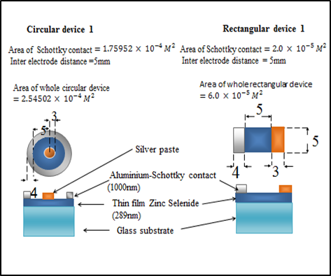 | Figure 1. Device dimensions for rectangular and circular devices |
2.1. Electrical Analysis
- By varying the voltage in steps of 0.1volts, the corresponding current was read from a Keithley 2400 Source meter connected to record current at room temperature. Graphs of current against voltage were plotted using Origin software.Circular and rectangular Schottky devices labeled according to the Schottky contact area were characterized. Circular device 1 (area 1.75952 × 10⁻⁴m2) and circular device 2 (area 2.0423×10⁻⁴m2) I-V characteristics were compared. The same was done for Rectangular device 1 (area 2.0×10⁻⁵m2) and rectangular device 2 (area 2.5×10⁻⁵m2).
3. Results and Discussions
- A graph showing forward I-V characteristics of the circular and rectangular devices is shown in figure 2. It can be seen that the I-V characteristics are rectifying in nature. This indicates the existence of a potential barrier between the thin films of Aluminium and n-type ZnSe. At low voltages ˂ 1volts, conduction mechanism is ohmic [3]. At voltages between 1V and 4V, a square law is observed (I α V2) It can be seen that circular device 2 with large Schottky contact area has better rectifying properties than for the same type, but with smaller area. The same can be seen for rectangular devices. This can be attributed to reduced contact resistance as area increases. This also enhanced the forward conduction of the Schottky region in the rectifier and resulted in the majority of current being transported via the Schottky region [4].
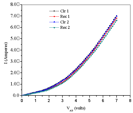 | Figure 2. Effect of contact area and geometry on dark forward I-V characteristics |
 of a Schottky diode of saturation current
  and diode ideality factor
  are related by [5]:
 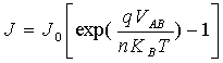 | (1) |
 to zero when
  ; and
; and  is the applied voltage.
 | (2) |
 | (3) |
 across the diode can then be expressed in terms of the total voltage drop V across the series combination of the diode and resistor therefore
  [6]. A plot of
  versus applied voltage
  ; for circular devices is shown in fig 3.
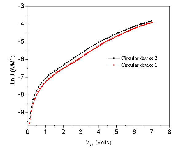 | Figure 3. Effect of area on circular metal contacts on Ln J characteristics |
|
4. Conclusions
- Deposition of ZnSe thin films was done by thermal vacuum evaporation method. Fabrication of metal-semiconductor devices was successfully done, and from their
 versus V characteristics, the diode ideality factor was seen to range between 6.361 ± 0.01 to 6.512 ± 0.01 for circular devices and 7.269 ± 0.01 to 7.318 ± 0.01 for rectangular of film thickness 289nm. It can be concluded that devices with larger metal contacts and thus shorter inter electrode spacing (device 2) have the lowest diode ideality factors and thus better electrical characteristics.