-
Paper Information
- Paper Submission
-
Journal Information
- About This Journal
- Editorial Board
- Current Issue
- Archive
- Author Guidelines
- Contact Us
Microelectronics and Solid State Electronics
p-ISSN: 2324-643X e-ISSN: 2324-6456
2013; 2(4): 59-64
doi:10.5923/j.msse.20130204.01
An Accurate Method for Extracting the Three Fowler- Nordheim Tunnelling Parameters Using I-V Characteristic
 Abstract
 Reference
 Full-Text PDF
 Full-text HTML
A. Latreche
Département des Sciences de la matière, Université de Bordj Bou Arreridj, 34000, Algérie
Correspondence to: A. Latreche, Département des Sciences de la matière, Université de Bordj Bou Arreridj, 34000, Algérie.
| Email: |  |
Copyright © 2012 Scientific & Academic Publishing. All Rights Reserved.
In this work, we have developed an approach for determining the electrical Fowler-Nordheim parameters such as the barrier height ( ), the correction term (
 ) relating to work-function differences between the oxide-facing surfaces of the metal gate and the semiconductor, and to any band-bending effects as well as the series resistance (R). In this method the barrier height has been extracted from both the classical parameters A and B in the case
  . The correction term (
 ) is considered as a parameter, not assumed or ignored. This method is proved to be useful and of a great interest after being tested.
Keywords: MOS Device, Extraction, Parameters, Fowler-Nordheim
Cite this paper: A. Latreche, An Accurate Method for Extracting the Three Fowler- Nordheim Tunnelling Parameters Using I-V Characteristic, Microelectronics and Solid State Electronics , Vol. 2 No. 4, 2013, pp. 59-64. doi: 10.5923/j.msse.20130204.01.
1. Introduction
- The elementary structure used in the majority of electronic devices such as field effect transistors and EEPROM memories is the metal-oxide-semiconductor (MOS) structure[1]. A fundamental process in the description of the current–voltage (I–V) characteristic of a metal - oxide - semiconductor structure is the advent of Fowler –Nordheim (F-N) tunneling[2]. The F-N formula has been widely used to explain clearly the conduction behavior in the conventional SiO2 films[3].Values for Fowler–Nordheim (F-N) tunnelling parameters, A and B, are important in the simulation of circuits where floating-gate transistors (FGMOS) are used, as they are related to artificial neural networks, pattern recognition circuits, offset trimming[4, 5]. The parameter B is mainly sensitive to the oxide field. Therefore, an accurate determination of the oxide field is necessary for the accurate determination of the parameters A and B. This will in turn give a correct value of barrier height. This can be done by choosing a thick oxide, and correcting the oxide voltage by the flat-band voltage[6]. The extraction of the F-N parameters is still under discussion, contributing to the extraction of theoretical and experimental parameters. Accurate knowledge of these parameters is necessary to explain the conduction in the conventional SiO2 films. According to the F-N model[7], the current that flows through a thin dielectric layer when a field F is applied reads:
 | (1) |
 | (2) |
 | (3) |
 1.5414 μA eV V–2] and b[
 6.8309 eV–3/2 V nm–1] are the Fowler-Nordheim Constants,
  is the energy -barrier height for tunnelling from the cathode into the oxide. Equations (2) and (3) can be inverted to give
 | (4) |
 | (5) |
 | (6) |
 is a correction term relating to work-function differences between the oxide-facing surfaces of the "metal" gate and the semiconductor, and to any band-bending effects that may be present. R is the series resistance (in the electron path between the contacts) that is due to effects other than tunnelling.In the literature, the "classical method" derives the barrier height,
  from the parameter B because the parameter B is the dominant parameter determining the current flow in the gate oxide.However, it is known that the value of B extracted from a F-N plot made in terms of the applied voltage V (rather than oxide field F) is affected by the values of the correction term (
 ) (see Fig. 2) and by the series resistance (R)[8, 9]. Normally, the largest component in
  for thick oxides is the so-called "flat-band voltage" VFB, which relates to the work-function differences between the oxide-facing surfaces of the "gate" and the "substrate". This flat-band voltage is determined by the band-structures of the gate and substrate, and is influenced by the presence of trapped charge. Generally, its value is extracted from capacitance voltage (C–V) measurement and depends on the manufacturing conditions of the device[15]. Accordingly, any device has its own correction term (
 ). In addition, the barrier height (
 ) extracted from the parameter A is very discrepancy than the extracted from the parameter B. A comparison between several values of
  and
and  previously published is presented in Table 1. From the listed values, the barrier heights (
 and
and  ) obtained for each device are significantly different.
|
 and
and  previously published in the literature
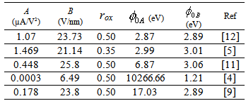
 is often assumed or ignored during the extraction of
  . Chiou[11] in his work, reported that a difference of 0.95 V in VFB leads to the change of 25 % in the parameter B. So, the value of
  has changed drastically. This consistency issue raises serious question on the validity of
  extracted using the ''classical method''. In conclusion, the accurate knowledge of the value
  and R is very important for determining the oxide field, and hence the barrier height
 . In this study, by taking into account all the concerns mentioned above, we have proposed a simple method for extracting the Fowler-Nordheim parameters from I-V characteristic. This method uses both parameters A and B at the same time and improves the “classical method” which is based on the parameter B only. In order to show the methodology of our proposed method, we used experimental data published previously[8]. In this experimental study, MOS capacitors with oxide thickness tox = 4.9 nm and square areas (S) ranging from 10-5 to 10-3 cm2 were used. The substrate is p-type (100) Si with a doping concentration of about 1015 cm-3. The oxidation was carried out in a dry N2/O2 atmosphere at 800°C. Poly-Si gates 350 nm-thick were deposited by LPCVD and subsequently n+ doped by POCl3 diffusion at 900°C. Measurements were performed at room temperature and dark conditions. Negative voltages were applied to the gate with the substrate contact grounded (for more details see[8]). The typical I–V characteristics for different gate areas ranging from 10-5 to10-3 cm2 are shown in Fig. 1.
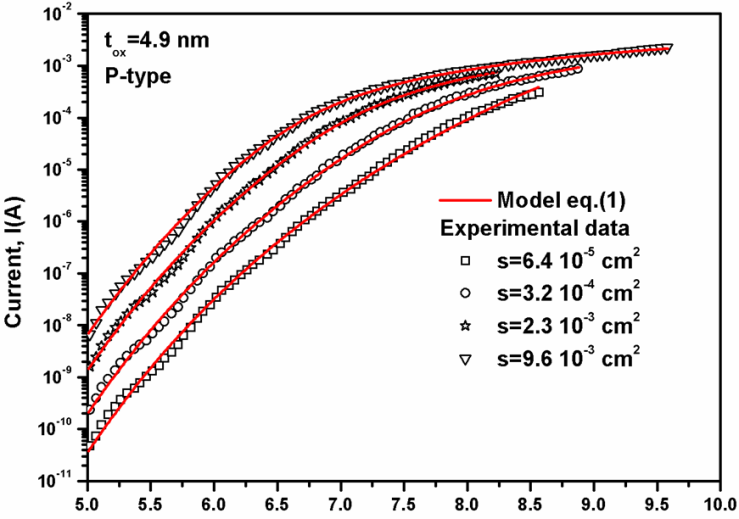 | Figure 1. Current–voltage characteristics (from reference[8]) for different gate areas ranging from 10-5 to 10-3 cm2. The symbols correspond to the experimental data whereas the solid lines correspond to the simulated I–V curves using eq.(1) with our extracted parameters reported in the table 2 |
 on the F-N plot, and hence on the parameters A and B. However, the linear relation in F-N plots is unaffected.
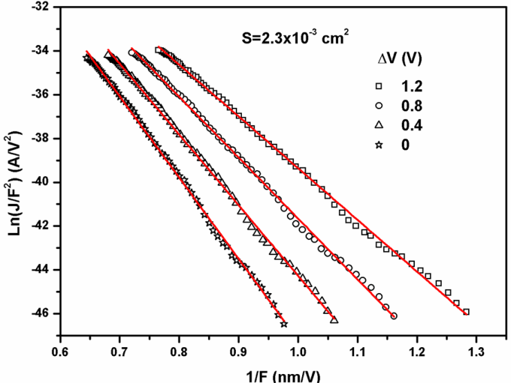 | Figure 2. The effect of uncertainty of the correction term  for the gate area S=2.3x10⁻³ cm2 with R=883 Ohm for the gate area S=2.3x10⁻³ cm2 with R=883 Ohm |
2. Intersection Point Method (IPM)
- This method is based on the Fowler-Nordheim plot. The idea of this approach is very simple. For each given resistance (R) we follow these two steps: 1- First, we vary the flat band voltage, then we extract the two barrier heights
 and
and  from the parameters B and A respectively by using a linear least-squares fitting procedure of the transformed data
  . The convergence of the first step of the program occurs when the two barrier heights are equal (
 ). The simple least squares regression model determines the straight line that minimizes the sum of the square of the absolute errors. It can be shown that this occurs when the slope B of the line and A the y-axis intercept are given by[16]
 | (7) |
 | (8) |
 are the mean of the measured x and y data and N is the number of data pairs (xj, yj). In our case Ln(I/SF2) represents y axis and 1/F represents x axis.
 | Figure 3. Intersection of the two curves of   against the correction term ( against the correction term ( ) at various resistances for the MOS structure area S=9.6x10⁻³ cm2 ) at various resistances for the MOS structure area S=9.6x10⁻³ cm2 |
 and
and against the correction term
  at various resistances. The point of intersection of the two curves gives the two initial parameters
  and
and  in addition to the third initial (input) parameter R. It is clear from this figure that the values of
  and
and  depend on the value of the resistance R. The barrier height,
  varies slightly and linearly with
  whereas the barrier height
  varies rapidly. This result confirms that the parameter B is predominant but is not sufficient to determine the barrier height
 . For this purpose, we need the parameter A to determine the correct value of barrier height
 . This occurs when the value of
  equals
 .
.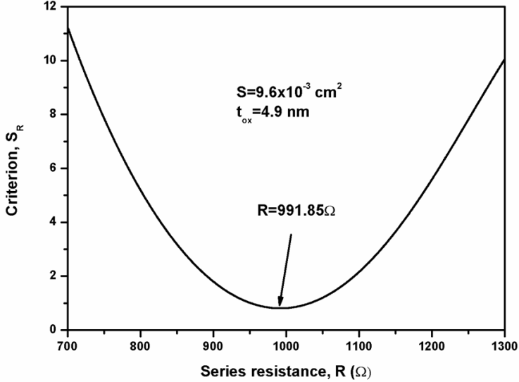 | Figure 4. The sum of the quadratic relative errors against series resistance for the MOS structure area S=9. 6x10⁻³ cm2. The effective mass of the electrons in the oxide has been assumed, m*= 0.5m |
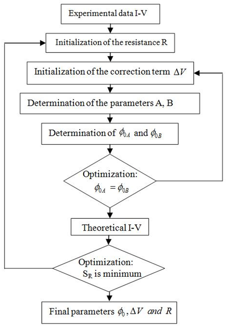 | Figure 5. Algorithm for the determination of F-N parameters by the intersection point method |
 ,
, and R) which verify the best fit of the experimental variables (I,V), we use the criterion (SR) that presents the quadratic relative errors and should be minimum (Fig. 4). This criterion was proposed for the first time by Osvald[17] for extracting the Schottky diode parameters from forward I-V characteristic.
 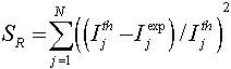 | (9) |
 is the ith experimental value,
  is the fitting value of the current, i.e. given by solving the equation (1) by using Newton's iteration method with the extracted initial values (
 ,
, and R) selected in the step 1. This second step is not necessary for thick oxides because the term “RI” in equation (6) can be ignored, as it is negligible compared to
 . Fig .5 summarizes the methodology of F-N parameters extraction by the intersection point method.The criterion SR exhibits a minimum as a function of R, as clearly shown in Fig. 4. In the particular case under investigation (S=9.6x10⁻³ cm2), the minimum of SR corresponds to the extracted parameters:
  = 3.228 eV,
  = 0.750 V and R = 991.85
 .The extracted parameters for all gate areas are presented in Table 2 and plotted as a function of the gate area as shown in Fig.6 and Fig.7.
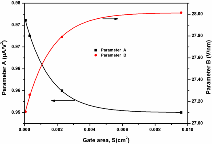 | Figure 6. Extracted parameters, A and B as a function of the gate area |
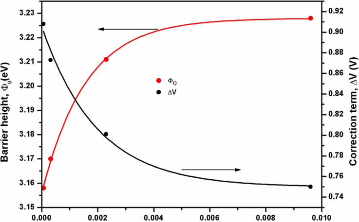 | Figure 7. Extracted parameters  and and  as a function of the gate area as a function of the gate area |
|
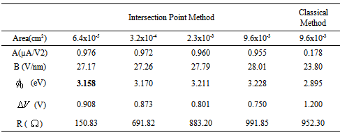
 are different from the assumed value (1.2 V). If we accept that the intersection point method gives the exact parameters, the uncertainties of 10%, 60% and 4% in the barrier height, the correction term (
 ) and the series resistance, respectively are estimated by the classical method for the MOS structure area S=9.6x10⁻³ cm2.The barrier height (
 ) and the parameter B are slightly increased with increasing the injection area, while the parameter A and the correction term (
 ) are decreased with increasing the injection area. Croci[12] in his work concluded that the gate geometry, the substrate (p or n) doping type, the nature of the tunnel oxide and the gate structure affect the F-N tunneling parameters (A, B,
  ), while this is not the case for the gate area.By analyzing of the curves in the Fig.6 and Fig.7 we have found that all the parameters (A, B,
  and
and  ) are varied exponentially with MOS structure area according to the following equation
 | (10) |
 in the eq.(10) is the dominant parameter determining the evolution of the all parameters (A, B,
  and
and  ). For the parameters A, B and
  the coefficient
  equals 1.57x10⁻³ cm2 while for the parameter
  equals 1.96x10⁻³ cm2. The parameter
  dependence on the gate area (decreases with increasing the gate area) can be probably explained by the trapped charge density that decreases with increasing the gate area. In turn, this trapped charge can be the origin of the increasing of the barrier height (
 ) because the exponential coefficients
  for both parameters
  and
and  are approximated.
3. Conclusions
- In conclusion, a simple method for extracting the three Fowler–Nordheim tunneling parameters using I-V characteristic parameters MOS device: the barrier height (
 ), the correction term (
 ) and the series resistance (R) has been presented. Our method called Intersection Point Method (IPM) is based on the Fowler–Nordheim plot with the condition
 . This method allows us to extract the correction term (
 ) due to the flatband voltage and potential drops at the electrodes by using current–voltage (I–V) characteristics and not assumed or ignored. Determining the correction term and the series resistance leads to know with accurate the oxide electrical field value.