Malek Ramezani1, Nima Ahmadpoor2
1Dept. of Electrical Engineering, Abadan branch, Islamic Azad University, Abadan, Iran
2Dept. of Electrical Engineering, Mahshahr branch, Islamic Azad University, Mahshahr, Iran
Correspondence to: Malek Ramezani, Dept. of Electrical Engineering, Abadan branch, Islamic Azad University, Abadan, Iran.
| Email: |  |
Copyright © 2012 Scientific & Academic Publishing. All Rights Reserved.
Abstract
Inthe start of this paper, a novel second generation current conveyor (CCII) with simple structure is presented. The proposed circuit has a rail to rail dynamic range in output and input terminals. Moreover, it is highly capable of driving currents in node z. This circuit works in class AB mode and is able to sink and source current in output node z+ and z- respectively. The CCII circuit was simulated in the standard 0.18μm CMOS TSMC technology with minimal count of CMOS transistors. The proposed circuit can be suitable for RF analogue structures such as filters, oscillators and sigma-delta modulators because of the high frequency performance for current and voltage transfer functions. In this circuit, the -3dB cut-off frequency of voltage and current transfer functions have been measured 3.8GHz and 3.2GHz respectively. In the remainder of the article a universal current mode filter is designed and simulated by sub base structure of the suggested CCII circuit. This universal filter can employ low pass, high pass and band pass which can adjust the cut-off frequencies and quality factors by variation of grounded resistor values. The cut-off frequencies of filters are about 300MegHz. Another good characteristic of filters is a low sensitivity to variation of passive component.
Keywords:
Current Conveyor, Current Mode, Low Voltage, Rail to rail, Universal filter, Cut-off frequency
Cite this paper: Malek Ramezani, Nima Ahmadpoor, New Current-mode Universal Filter by a Novel Low Voltage Second Generation Current Conveyor, Microelectronics and Solid State Electronics , Vol. 2 No. 3, 2013, pp. 52-57. doi: 10.5923/j.msse.20130203.03.
1. Introduction
The basic structure of second generation current conveyor (CCII) was first expanded by Sedra and Smith in 1970[1] and today, one of the state-of-the-art subjects which is considered by analog current mode circuit researchers is development in performance parameters of CCII circuits. The results of their investigations have led to resolution increasing in current and voltage transfer functions, compensation of offset[2], improvement in transfer functions linearity[3] and high frequency features[4], optimization circuit toward low power and low voltage design[5] and trend for differential circuitry. Among these goals, the low power and low voltage circuitry and improvement the linearity range of CCII transfer functions are widely applicable for VLSI and current mode circuit design. Moreover, high frequency performances of CCII can be applied greatly in mobile communication analog structures.In this paper, the classical unity gain current conveyor with symmetric current direction in output nodes has been presented. The parameters of linearity boundary, frequency response and low voltage requirements have been improved in comparison with other similar works. Moreover, the simple and differential structure of proposed CCII is another advantage of offered circuit[6].Current conveyors often use both current mode and voltage mode analog structures. However they present a wider dynamic range, better frequency performances and especially a lower voltage and power consumption in current mode structures as compared to voltage mode counterparts. Thus the recent developed circuits of CCII are more applicable as one of the basic active elements in current mode analog interfaces such as filters, VCOs and data converters[7]. Especially one of the common usages of CCIIs is current-mode universal filters[8, 9]. Classical unity gain current conveyor can be used for the formation of universal filters to achieve a simpler structure and lower power dissipation[10]. Employment of double negative and positive output current nodes can be a better choice for the flexibility sufficiency in implementation of universal current mode universal filters[11].In the remainder of paper the universal current mode filter is implemented by two CCIIs and five passive elements. The number of active has been optimized element in proposed circuit and as can be seen in simulation result, the cut-off frequencies and quality factors can be simply changed by variation of R1 and R2. This feature can establish digitally programmable implement capability by switches and logic pins. The proposed universal filter exhibits high frequency performances. As shown in simulation result, the high and low cut-off frequencies around several hundreds of MHz frequency.
2. The Proposed CCII Circuit
Current conveyors are basic and applied active components in analogue interfaces and elementary signal processing cells especially with the current mode configuration. Basic construction of ideal CCII is formed by three ports, x, y and z. The model of CCII can be introduced by negative or positive styles with regard to output current direction which can be internal or external at node z. Figure 1 shows the blocked style of dual positive and negative implementation.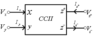 | Figure 1. The block diagram scheme of the positive CCII |
The CCII can be explained by two sub-circuits: voltage followers and current-mirrors.Both current mirrors’ gain and voltage followers’ gain are one in the unity gain CCII. As a result, the equations of unity gain dual output current nodes type of CCII are given by: 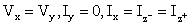 | (1) |
Currents and voltages that are applied in above equations have distinguished in schematic of figure 1. The offered circuit of CCII which its dimensions are optimized for high frequency and can be used in RF analog structures is shown in the figure 2. The proposed circuit is implemented in the standard 0.18μm CMOS TSMC technology. Furthermore its configuration presents low voltage, rail to rail and high linearity features. Therefore dual differential pair of PMOS and NMOS transistors has been chosen for the input stage (M8, M9, M10 and M11) that can provide the rail to rail specification. As Figure 2 shows, the M8 and M11transistors prepare the input positive amplitude;besides, the M9 and M10transistors prepare the negative one. In this design active load of voltage follower stage is created by NMOS transistors (M14, M15) and PMOS transistors (M2, M4) as current mirrors. Consequently, the bias currents in dual lines of voltage follower stage are equal and it lead to same voltages at nodes x and y.As shown in Figure 2, the M5, M6, M16, M17 current mirrors use for equalization of current at node x with node z+ ; furthermore, the M18, M19, M20, M21, M22, M23 current mirrors use for the same currents with opposite direction at node z. 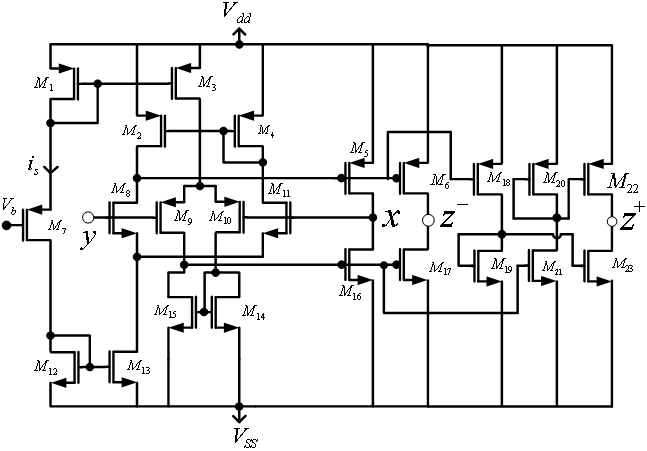 | Figure 2. The schematic of suggested CCII circuit |
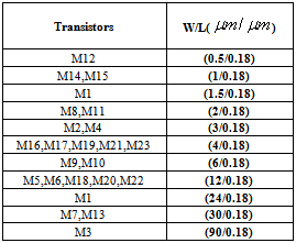
The proposed low voltage and high frequency CCII is simulated in the standard 0.18μm CMOS TSMC technology. The HSPICE software has been used for simulation and the dimensions of CMOS transistors which are used in simulation, has been set in the table 1. The suggested CCII is composed of dual symmetric supply voltages ±0.75V that it indicates the low voltage characteristic. Figure 3 shows the linear relation between voltages of terminals x and y, which identified the linearity specification of voltage transfer function. As shown in this figure, voltage in node x tracks the voltage in node y from -0.7Volt to +0.7Volt with linear curvature. Thus, the rail to rail dynamic range of voltage variation can be employed.Table 1. the dimensions of CMOS transistor of proposed CCII
 |
| |
|
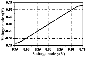 | Figure 3. the voltage at node x versus the input voltage of node y |
Figure 4 shows the linear relation between internal and external output current of terminals z+ and z- versus the internal current of terminal x. these current transfer functions prove the capability of current drive in output stage of proposed CCII. The voltage and current transfer function carves according to the Figures 3 and 4 have unit slope Because of the unity gain design. As calculated the voltage and current transfer function variations errors are less than 1%.In this circuit, the -3dB cut-off frequencies for voltage and current transfer functions are 3.87GHz and 3.23GHz respectively. Figure 5 shows the frequency response of voltage transfer function. Since, the high frequency performances feature of proposed CCII, it has been able to use in analog RF components.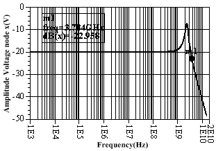 | Figure 5. frequency response of voltage transfer function |
3. The Proposed Universal Filter
Nowadays, One of the most attractive analog RF component are filters which can employ a higher frequency performance and lower power consumption, For reaching to this goal a current-mode circuitry is a better choice structure method than the voltage-mode counterpart. In this research, the second order analog current-mode universal filter has been designed and implemented in new structure as shown in figure 6. It employs low-pass (LP), high-pass (HP) and band-pass (BP) filters by single-input current  and triple-output current
  As shown in figure 6, the presented circuit current-mode universal filter has been realized from two CCIIs, two capacitors and two resistors. Consequently it has simple structure with minimal count of transistors. In addition the structure presents low power and high-frequency respond because of minimal active and passive elements and optimization of CCII’s circuit for a high frequency performance. The voltage transfer function of the non-ideal unity gain second generation CCII can be supposed by equation (2) as flowing:
 | (2) |
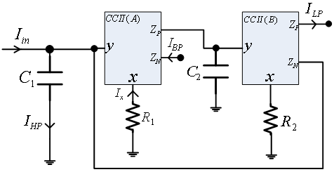 | Figure 6. Proposed current-mode universal filter with single-input three-output |
By applying small signal analysis of the proposed universal filter, the theoretical expressions of triple current transfer functions can be approximately given by: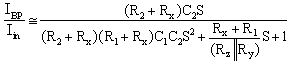 | (3) |
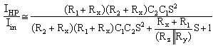 | (4) |
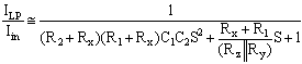 | (5) |
In above equations 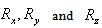 are parasitic resistance at port x, y and z of CCII respectively. These Equations can verify the implementation of band pass, high pass and low pass current-mode filters theoretically. Also,the natural frequency and the quality factor of the proposed universal filter can be obtained as:
 | (6) |
 | (7) |
4. Simulation Result
In order to investigate the theoretical results of the proposed universal filter, Hspise simulations have been performed. At the first, the unity gain translinear CCII in figure 2 has been simulated with the transistor parameters ofthe standard 0.18μm CMOS TSMC technology. Afterward it was used to configure the universal filter in figure 5. The circuit in figure 6, was biased with ±0.75V supply voltages and element values  ,
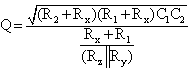
,  These values obtain unity gain transfer functions for universal filter approximately. Figure 7 shows the frequency responses of lowpass (LP), highpass (HP) and bandpass (BP) filters. The band widths of LP and BP filters have been evaluated 282.3MHz and 308MHz respectively. As well as, the central frequency of BP filterhas been measured 278.3MHz. Similarly, simulation results exhibit the low cut-off frequency 351MHz for HP filter.
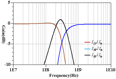 | Figure 7. Simulated frequency characteristics of LP, BP and HP of the proposed universal filter |
 | Figure 8. Input and outputs of BP filter at 300MHz |
The total power consumption of proposed circuit is 1.5mw which it confirms a lower power implementation in comparison with other same work. Also By variation of resistors  in figure 6 by digital calibration logic, we can change the cut-off frequencies and bandwidths of filters. Figure 9 shows the simulated frequency response of a BP filter when the resistances
  were simultaneously adjusted for the values 50, 150, 250, 350 and 400
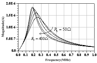 | Figure 9. Simulated frequency responses of the BP filter when  is varied is varied |
5. Conclusions
In this paper, a second generation current conveyor (CCII) with CMOS transistors was designed. The proposed CCII has rail-to-rail linearity range in voltage and current transfer functions, wide range bandwidth and low-voltage circuitry. The proposed circuit can be widely applicable in VLSI circuits, current mode analog components, and RF telecommunication circuits. In the remainder of paper the current-mode universal filter has been implemented by use of CCIIs as active elements. The circuit show highly performance in feature of low-power, high-frequency and low complexity. It employs lowpass, highpass and bandpass filters in en bloc structure with minimum count of transistors and specially can be useful for current-mode analog interfaces and RF applications.
References
| [1] | A. Sedra, K. Smith, “A Second-Generation Current Conveyor and Its Applications”, IEEE Trans. on Circuits Theory, CT-17, February 1970, pp. 132-134. |
| [2] | H. O. Elwan, A. M. Soliman, “A Novel CMOS Current Conveyor with an Electronically Tunable Current Mode Filter Suitable for VLSI”, IEEE Trans.on Circuits and Systems-II, Vol. 43, No. 9, Sept. 1996, pp. 663-670. |
| [3] | G. Palmisano, G. Palumbo, S. Pennisi, “Design Strategies for Class A CMOS CCIIs”, AnalogIntegrated Circuits & Signal Processing, Vol. 19, No. 1, pp. 75–85, Apr. 1999. |
| [4] | N. B. El Feki,S. B. Salim and D. S. Masmoudi, “Optimization of a Rail to Rail Low Voltage Current Conveyor and High Frequency Current-mode Filter Applications”, Journal of Applied Sciences Research, Vol. 4, No. 12, 2008, pp. 1925-1934. |
| [5] | H. O. Elwan, A. M. Soliman, “Low-Voltage Low-Power CMOS Current Conveyors”, IEEE Trans.On Circuits and Systems-I, Vol. 44, No. 9, Sept. 1997, pp.828-835. |
| [6] | N. Ahmadpoor, S. Mohamadzade, M. Ahmadzadeh, “A Novel Linear Low Voltage Rail to Rail Second Generation Current Conveyor for RF Applicationsˮ, Journal of Basic and Applied Scientific Research, Vol. 2, No. 12, 2012, pp. 12306-12310. |
| [7] | E. Farshidi and N. Ahmadpoor, “A Continuous Time Sigma Delta Modulators Using CMOS Current Conveyors”, World Academy of Science, Engineering and Technology , Vol. 78, June 2011, pp. 231-234. |
| [8] | J. W. Horng, “Voltage/Current-Mode Universal Biquadratic Filter Using Single CCII+ˮ, Indian Journal of Pure & Applied Physics, Vol.48, October 2010, pp. 749-756. |
| [9] | H. P. Chen, “Versatile Current-Mode Universal Biquadratic Filter Using Plus-Type Dual-Output ICCIIsˮ, Indian Journal of Pure & Applied Physics, Vol. 50, March 2012, pp. 188-198. |
| [10] | J. W. Horng, Zh. R. Wang and Ch. Ch. Liu, “Voltage-Mode Lowpass, Bandpass and Notch Filters Using Three Plus-Type CCIIsˮ, Circuits and Systems, Vol. 2, Published Online January 2011, pp. 34-37. |
| [11] | M. Kumngern, “Multiple-input single-output current-mode universal filter using translinear current conveyorsˮ, Journal of Electrical and Electronics Engineering Research, Vol. 3, No. 9, November 2011, pp. 162-170. |
 Abstract
 Reference
 Full-Text PDF
 Full-text HTML