-
Paper Information
- Previous Paper
- Paper Submission
-
Journal Information
- About This Journal
- Editorial Board
- Current Issue
- Archive
- Author Guidelines
- Contact Us
Microelectronics and Solid State Electronics
p-ISSN: 2324-643X e-ISSN: 2324-6456
2013; 2(3): 45-51
doi:10.5923/j.msse.20130203.02
Low Power Bus Encoding Techniques for Memory Testing
 Abstract
 Reference
 Full-Text PDF
 Full-text HTML
Balwinder Singh1, Arun Khosla2, S. Bindra. Narang3
1Centre for Development of Advanced Computing (CDAC), Mohali, India
2ECE Department Dr. B .R. Ambedkar National Institute of Technology, Jalandhar , India
3Electronics Technology Department, Guru Nanak Dev University, Amritsar, India
Correspondence to: Balwinder Singh, Centre for Development of Advanced Computing (CDAC), Mohali, India.
| Email: |  |
Copyright © 2012 Scientific & Academic Publishing. All Rights Reserved.
Power reduction during testing is one of the most important challenges for the VLSI design and test engineers. Switching is one of the important contributors to the power consumption of on chip buses. This paper addresses the problem of minimizing power dissipation due to switching of the busses during testing. For memory testing, many read/write cycles are required (as per March algorithm), in which test patterns are sent through the data bus, according to the addressing sequences. The address switching is also controlled by address encoding schemes with reference data. The result shows the average power reduction of 30% and 74.8% in data bus and addresses buses encoding schemes respectively.
Keywords: Low Power Encoding Scheme, T0-C code, Bus inverting Automatic Test Pattern Generator
Cite this paper: Balwinder Singh, Arun Khosla, S. Bindra. Narang, Low Power Bus Encoding Techniques for Memory Testing, Microelectronics and Solid State Electronics , Vol. 2 No. 3, 2013, pp. 45-51. doi: 10.5923/j.msse.20130203.02.
Article Outline
1. Introduction
- Power consumption has become one of the most critical issues during the design of battery operated portable systems. Design methodologies and related tools enabling the control on the power budget during the different phases of the design flow are mandatory. The main components of such portable systems are processing unit, the memory controller, memory chips. It is anticipated that the embedded memory will account for 95% of the chip area in the complex systems[1] and the communication channels which provide data transfer between the CPU and the memory. During thecommunication of these components bus power consumption is proportional to the switching activity. The switching activity of the buses is often responsible for a substantial fraction of the total power dissipation for large VLSI modules. As the compelxity of the system increase the number of data buses and address buses incresses. The large and long interconnects dissipates as dynamic energy dissipation for charging and discharging of internal node capacitances and inter-wire capacitances.Testing of the memory sections is a tedious job because in memory testing the bunch of the data is written and read again and again for all the memory locations at very high speed. During memory testing power dissipation increase drastically due to excessive switching in test patterns. Therefore, it needs low power encoding techniques for communication between devices or on chip communication. To access a Memory Under Test (MUT) address buses are required to access memory locations and data buses for sending test patterns. Thus, the minimization of the transitions can provide significant savings on the overall power budget. To accomplish this job there is a need of very fast processors which are connected in parallel to provide the very high testing rate. SCAN based design are mostly preferred for memory testing[1]. During writing and scanning first, write 0s to the memory in ascending order of address. Second, read the memory (expect to read a 0) and then write a 1 in ascending order of address and third is to read and write a 0 in descending order of address. Finally Fourth, read the memory (expect to read a 0). However testing time of a scan system is proportional to both the number of test patterns and the number of flip-flops in the scan chain(s). In a modern VLSI circuit, the numbers of internal flip-flops are in the range of thousands or even higher, therefore, to reduce test application time and large amount power consumption become an important issue, that needs to be optimized along with speed and area. Power consumption is directly related to the number of times flip-flops toggle their states i.e. toggling rate, so intention is given to arrange the test vectors in such a manner that minimum toggling occur in a Memory Under Test (MUT). Thus, the minimization of the transitions can provide significant savings on the overall power budget. The relation between power and switching rate is related according to equation 1.
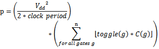 | (1) |
 represents biasing voltage, C(g) is the output capacitance of the nodes and toggle(g) is switching of the gates ‘g’.VLSI circuits with large power dissipation require expensive packaging to ensure appropriate heat dissipation. Excessive power dissipation results the overheating of the MUT, and probability of damage are increased at testing time. Thus most research efforts have focused on reducing the dynamic power consumption during memory writes and read cycle by reducing the transitions. The rest of the paper is organized as follows: In the next section, we reviewed the related work on the bus encoding schemes for low power. In section 3, the Bit Invert, Bit invert signaling, ABIT and Proposed Scheme for power reduction during the data are explained. Then the encoder and decoder are designed for these schemes and implemented on FPGA. In section 4, the address encoding schemes are discussed and implemented for the memory addressing. In section 5, we have compared these schemes on the basis of power, Area & energy efficiency for the reference data. In the last section conclusion is drawn.
2. Related Work
- Luca benini et. al.[3] presents the low power address bus encoding technique to sort out the problem of power dissipation for intellectual proprietary core processor. Here reduction in bus activity is achieved with this technique. Yazdan Aghaghiri et. al.[18][4] in this T0 and Offset- XOR encoding techniques are discussed and irredundant bus encoding for low power is presented and its benefit over the other techniques are presented, and it is shown that this method of irredundant saves 83% of power. Prabhat K. Saraswat et. al.[13] uses gray code and T0 code for memory address bus encoding. Bits encoded n such way the bit switching activity is reduced on the address busses. The sequences of addresses are generated of specified sequentialty and evaluated the performance of both codec’s.Sathish et.al[10] suggested a Efficient Switching Activity Reduction Technique for Fault Tolerant Data Bus for Deep-submicron (DSM) systems. The proposed encoding technique reduces the switching activity by 18% to 22.5%. Its efficiency is 8% to 15% more compare to others encoding techniques. Youngsoo et.al[8] presents a partial bus-invert coding scheme for power optimization of system level bus. In the proposed scheme, they select the sub-group of bus lines for bus encoding to reduce the total number of bus transitions. It reduces the total bus transitions by 62.6% on the average, compared to that of the unencoded patterns.Ghoneima et. al[22] proposed a low power on chip the serial-link bus (SLB) architecture which reduces the number of bus lines of the conventional parallel-line bus (PLB) architecture by multiplexing each m-bit onto a single line. In another paper , Sinha et.al[23] authors have proposed a bus encoding technique using Forbidden Transition Free Algorithm for Cross-Talk Reduction for On-chip VLSI Interconnect.
3. Data Bus Encoding Technique for Memory Testing
- Bus-Invert Method: This technique is based on Hamming Distance between the consecutive test vectors. Test patterns generated by the Automatic Test Pattern Generation (ATPG) are encoded according to their hamming distance before it sends to Circuit Under Test (CUT). The encoding depends on the Hamming distance between the value of the encoded bus lines at time t-1 (also counting the redundant line at time t-1) and the value of the bus lines at time t. The bus-invert encoding method can be expressed by the following equations[5]]2]:
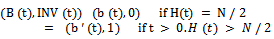 Where B (t) is the value of the encoded bus lines at time t,INV (t) is the additional bus line, b (t) is the address value at time t,
  is the Hamming distance, and N is the bus width of b (t).The corresponding decoding scheme is simply defined as:
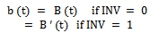 Major drawback of this approach are related to the required redundant bus line and the overhead due to the logic to implement the voter to decide whether the Hamming distance exceeds N / 2.Bus Invert Transition Signaling: With transition signaling a logical 1 is represented by a transition (from HI to LO or LO to HI) while a 0 is represented by the lack of such a transition. Transition signaling will not reduce switching activity by itself[5]. If transition signaling is used and at the same time we reduce the number of 1’s in the code words we can directly reduce the switching activity on the bus.Transition signaling combined with bus-invert (BI) coding, is called BITS coding. BITS reduce the number of logical 1s transmitted over the bus,[4] that are responsible for all the high-to-low and low-to high transitions, while the logical 0s are represented by the lack of transitions.In BITS encoding, if the number of ones in the incoming data is larger than half the bus width, then each bit of incoming data is inverted and INV is set to one (1) and then transition-encoded. Otherwise, each bit of incoming data is transition-encoded without alteration. More precisely, for a pattern at time, (Xi), its BI-encoded version is given by:
 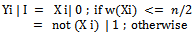 where | denotes a concatenate operation, I denote the value at the invert line, w (Xi) denotes the number of 1’s in Xi, and n denotes the bus width. Then, the BITS-encoded version of Xi is given by
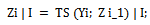 where TS(x; y) denotes a transition encoding of x with respect to y.The decoding process can be carried out by
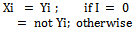 where
where  Note that both TS(x; y) and its inverse TS-1 (x;y) can be implemented by XORing x and y In Approximate BITS encoding[8] technique, numbers of transitions are reduced as compared to the simple and BI (bit inverse) method. Due to which the total power of the circuit is reduced. Its application to real circuit design is limited by the extra bus line, which calls for change in pin out and interface specification of the original chip. As the main overhead comes from a majority vote, that decides whether to encode 1 or 0 as having a transition, we eliminate the voter by moving to another technique which is ABITS. In ABITS method, the guess relies on the MSB of each input bus. This means that MSB takes over the function of invert line thus eliminating the need for an extra bus line. In ABITS method, the output function Y is the XORing or XNORing depending upon the MSB of input data.
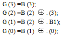
 Although ABITS encoding obtains less transition reduction due to incorrect guess, the overall power consumption (including the power consumed by the encoder itself) is fairly comparable to that of BITS encoding because the ABITS encoder consumes less power than BITS encoder.Proposed Technique for Encoding: The proposed technique has an edge over other existing techniques that it has no redundant line. Due to which an extra expensive pin is saved. This technique works for all data streams except for the stream containing all 1’s.EncoderIn this technique the encoder is used for encoding the transitions. It takes 8-bit input word as input bit stream and functions as:
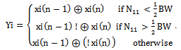 .Decoder The decoder is used for decoding the output generated from the encoder. It takes transmitted word as input bit stream and then computes the original input word X(n). It functions as:
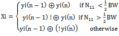 .Encoding function should minimize the average number of ones at its output while the encoded value Y(n) can still be uniquely decoded by D.
4. Address Bus Encoding Technique for Memory Testing
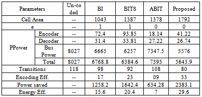
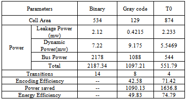
- In memory testing read /writes operations are performed according to the algorithms such as March. One address generator is also required for the addressing the memory locations. In this switching also takes place, causes the power dissipation. This switching can be reducing with various address encoding techniques. To encode the address bus for test with least switching activity various methods like gray encoding and T0-C encoding. By utilizing the sequential addressing instead of using random addressing reduces the power dissipation in the address line by reducing the toggling count. But after some clock cycles even the in the sequential addressing the toggling count is increased by the unity value. Due to that here we concentrate on T0, gray code base addressing and irredundant bus encoding. In gray encoding the toggling count is fixed to the unit value, which saves the power dissipation. To even reduce the toggling value beyond the unit value the technique preferred is the T0-C encoding. To save more power, instead of using gray coding T0-C encoding is used. In case of simple T0 encoding the process of sending address bit is shown in table1, below:
|
|
 The gray code counters are popular in digital system for a variety of applications, such as representing the state variables in state machines or acting as pointers in First-In First-Out (FIFO) memories, and also can be used as address counters. This is because in gray code counters only one output bit is ever toggling at a time in as opposed to multiple bits in a binary counter. These counters count the values in gray codes only. The advantage of Gray code counters over others is that they consume only half the power of an equivalent binary counter and correspondingly less noise.
5. Bus Power Model for Encoding Scheme
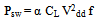
- Let us assume, power P watt will be dissipate when switching takes place in any of the bus line. System bus switching can be calculate for n bus lines then the power dissipation is n * P watt and so to calculate the switching activity[15]. The power dissipation on the bus is calculated by applying all the encoding techniques on the reference data as taken in Table 5. Power dissipation is given by:
 | (2) |
 | (3) |
 | (4) |
 | (5) |
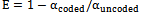
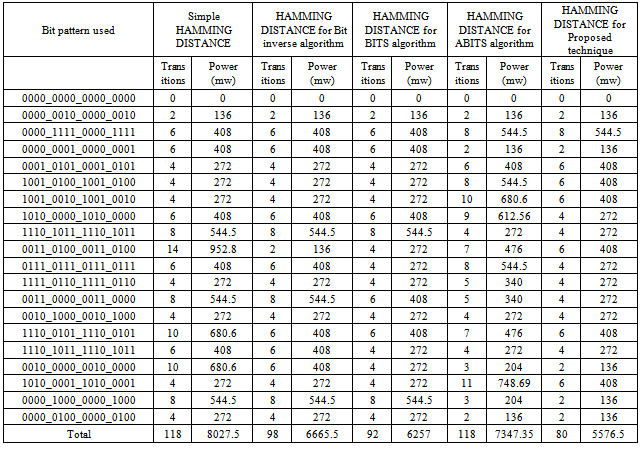
6. Experimental Results
|
|
|
|
7. Conclusions
- The low power bus encoding techniques play an important role in reducing the switching activity during the on chip communication. Testing of the memory is very important because 90% of the chip area is occupied by memory. During memory testing many read /writes operations needs to be test according to the March algorithms) to achieve 100% fault coverage. In this paper we have implemented bus encoding schemes for memory BIST. The encoding schemes are applied to the data bus and address bus by taking the reference data. The power consumption of various encoding schemes is shown in figure 1. It is observed from the results of proposed scheme for data encoding is 33% less switching activity occurs and about 30% of average power is saved. In case of address encoding that 71.2 % less switching activity occurs and about 74.8 % of average power is saved is shown in figure 2
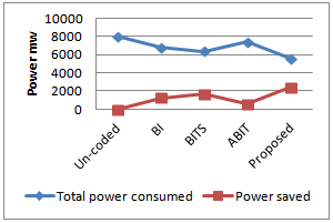 | Figure 1. Power consumption of Various Data Encoding Schemes |
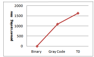 | Figure 2. Power consumption of Various Address Encoding Schemes |