-
Paper Information
- Previous Paper
- Paper Submission
-
Journal Information
- About This Journal
- Editorial Board
- Current Issue
- Archive
- Author Guidelines
- Contact Us
Microelectronics and Solid State Electronics
p-ISSN: 2324-643X e-ISSN: 2324-6456
2013; 2(2): 29-38
doi:10.5923/j.msse.20130202.03
Optimization of High Performance Bulk FinFET Structure Independent of Random Dopent Process Variations
 Abstract
 Reference
 Full-Text PDF
 Full-text HTML
S. L. Tripathi, Ramanuj Mishra, R. A. Mishra
Department of Electronics and Communication Engineering , MNNIT, Allahabad
Correspondence to: S. L. Tripathi, Department of Electronics and Communication Engineering , MNNIT, Allahabad.
| Email: |  |
Copyright © 2012 Scientific & Academic Publishing. All Rights Reserved.
FinFETs are multigate MOSFETs conventionally fabricated on SOI wafer. Alternatively, use of Si-bulk wafers for FinFET has gained significant interest for the low cost of wafers and more importantly for the compatibility with bulk CMOS technology. This paper describes the design of Bulk FinFET with improved performance using different bulk structures. In initial part of work, we have used the Pie- gate structure and heavy body doping structure i.e. Punchthrough stopper. Both the structures are combined in a novel Pie-gate bulk FinFET structure with punchthrough stopper. It has been observed that the novel structure shows better results compared to previous structures but it is difficult to fabricate. So, the Performance of bulk FinFET with bottom spacer is studied including the detailed discussion of process variation effect which shows that such bulk structure is supposed to have less fabrication complexity to achieve and optimize a desired doping profile. Finally, It is observed that the bulk FinFET with bottom spacer can be optimized to obtain superior performance than all other FinFETs making it independent of doping related process variations.
Keywords: Bulk (FinFET), Subthreshold Performance, Punchthrough Stopper, Bottom Spacer(BS), Active Fin Length, Width Quantization, SOI FinFET, Sentaurus TCAD Device Simulator
Cite this paper: S. L. Tripathi, Ramanuj Mishra, R. A. Mishra, Optimization of High Performance Bulk FinFET Structure Independent of Random Dopent Process Variations, Microelectronics and Solid State Electronics , Vol. 2 No. 2, 2013, pp. 29-38. doi: 10.5923/j.msse.20130202.03.
Article Outline
1. Introduction
- Conventionally FinFET[1] is fabricated on SOI wafer[2-3] because of its excellent short channel characteristics but SOI wafer shows some disadvantageous over bulk FinFET like floating body effect , heat transfer problem and high wafer cost[4]. Bulk FinFET[5] covers most of the drawbacks of SOI FinFET. Also, bulk FinFET shows better immunity to negative bias-temperature (NBT) stress[6]. Additionally, Bulk FinFET has gained attention due to its low-cost process and the ability to be integrated with standard bulk CMOS technology[7-8]. But the characteristics of bulk FinFET are not comparable with SOI FinFET. One major advantage of SOI over bulk is speed. SOI devices have 30% speed advantage over their bulk counterpart in normal MOSFET. But it has been reported[9] that owing to their geometry (i.e.3D structure) for significantly (~60nm) large Fin height, less than 5% delay difference is obtained. For Fin height of 30nm this delay difference becomes approximately 8%. Therefore, we can say that speed advantage in SOI FinFET is not prominent as it is in normal SOI MOSFET leading to the importance of bulk FinFET structures of comparable performance parameters.. The Bulk FinFETs are fabricated with high body doping to suppress source to drain coupling effect[10] However, the lack of isolation layer underneath the transistor body allows the drain field to penetrate towards the source more easily by deteriorating the subthreshold slope and DIBL. Use of high channel doping is used to reduce OFF state current to improve performance of bulk FinFET. But this will result in significant mobility degradation and high parasitic capacitances[9]. Although bulk FinFET shows excellent promise but it does not have performance as good as SOI FinFET. So, it is important to optimize bulk FinFET performance as in SOI FinFET. Previously, Pie-gate bulk FinFET i.e. isolation oxide with source/drain-to-body (S/D) junctions shallower than gate-bottom[11] and bulk FinFET of heavy body doping i.e. Punchthrough stopper, is reported[9]. Here Pie-gate structure is basically represented by misalignment(ΔXj=-ive) between the S/D junctions and the bottom of the gate electrode. Since the change of performance due to process variation can be very undesirable for some analog or digital CMOS circuits, the designer wants that the device performance should be independent of process variation[12]. The observed random distribution of identically drawn devices can be caused by impurity concentration densities. This results from non-uniform conditions during the deposition and the diffusion of the impurities(dopant) and the changes in these parameters cause electrical parameters to vary, such as sheet resistance and threshold voltage. It has been shown in [9] that the performance of bulk FinFET can be improved by use of punchthrough stopper doping and it can be observed that the performance of bulk FinFET is very sensitive to channel doping. Using FinFET with punchthrough stopper also require a precise control of doping and doping profiles[9]. In normal bulk FinFET, it is very difficult to optimize precise punchthrough stopper doping and also during fabrication, the process variables(like temperature) may cause undesirable change in performance. In our work we have used bottom spacer bulk FinFET structure to optimize the doping of punchthrough stopper. It has been shown in[13] that it is possible to have a optimized punchthrough stopper doping with the use of vertical doping, while using bottom spacer. Fabrication process of bottom spacer doesn't involve any tilted angle implant like we need in conventional structures. So BS is supposed to have less fabrication complexity to achieve and optimize a desire doping profile (punchthrough stopper doping ). Also it has been shown that while using bottom spacer structure our device performance becomes more independent of active Fin doping which indicate that we do not need a particular doping profile in bottom spacer FinFET. In other words, the performance become independent of process variation caused by impurity concentration densities which can be considered as a big advantage of bottom spacer structure. Also to deal with width quantization problem[14] as in SOI FinFET, Bulk FinFET structure with bottom spacer reported, is again important. We compare Bulk FinFET having bottom spacer with the previously reported heavy body doping and pie- gate bulk FinFETs. The effective channel width of triple gate FinFET is given by
 | (1) |
2. Device Structure and Simulation Setup
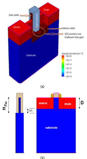
- The Bulk and SOI FinFET structures have been made with 3-D Sentaurus structure editor[16-17]. The tri-gate FinFET designed is of 32nm channel length with source/drain doping is 1E20 cm-3(n type). Metal is used as gate contact material and the work function of metal is kept 4.62eV. Silicon dioxide is used as gate oxide material with gate oxide thickness of 1.1nm. The channel doping is different for different simulations with VDD=1.0V. The FinFET is designed with 16nm spacer length, 10nm Fin width and 60nm Fin height. Pie gate SOI FinFET is reported in literatures[11] i.e. Fig. 1 shows a marked misalignment (ΔXj) between the Source/Drain junction depth and gate depth. This structure will be equivalent to Pie-gate structure if misalignment ΔXj is negative. For comparison point of view Source/Drain junction depth kept is constant (60 nm) and gate is penetrated deeper into bulk(Fig. 2).In second part of our work we have analysed Bulk FinFET with punchthrough stopper doping which is reported in ref[9]. We have doped pie gate Bulk FinFET with heavy body doping and made comparisons between all bottom spacer structure for FinFET which is reported earlier for SOI FinFET[13].In last part of our work we have made Bulk FinFET with bottom spacer. 3D view of device is shown in Fig. 3. In case of uniform doping profile, doping of entire bulk region is kept constant. Device is also simulated and optimized for different bulk doping profile. Side view of Channel region of Bulk FinFET with bottom spacer is shown in Figure. The Bulk portion beneath bottom spacer is called as inactive Fin and Bulk region surrounded by gate contact is called active fin.. Silicon dioxide is used as spacer material. The height of Fin is 60 nm. The Simulation is also done for different height of bottom spacers.
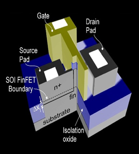 | Figure 1. 3-D View of Pie gate SOI FinFET(ΔXj negative) |
 | Figure 2. (a) 3-D view of Pie-gate Bulk FinFET structure (b) Cross-sectional view of pie gate FinFET structure |
 | Figure 3. (a) 3-D view of Bulk FinFET (b) Side view of Bulk FinFET (c) Side view with uniform and non uniform doping with bottom spacer |
3. Results and Discussion
3.1. Previously Reported Bulk FinFETs
- Conventional bulk FinFET with low channel doping (1E16) has DIBL of 371 mV/V and Subthreshold slope of 328 mV/Decade. High channel doping is used to get improved performance. Bulk FinFET with high channel doping (1E18) shows significant improvement having DIBL of 44 mV/V and subthreshold slope of 75 mV/decade. But high channel doping has its own drawback. To improve bulk FinFET performance high body doping is studied. Using low channel doping in active Fin(higher Fin) and high doping in lower Fin as well as body as reported in[13], significantly improves performance. Subthreshold slope of profile reported in[9] is 78 mV/Decade and DIBL of device is 46 mV/decade which is a significant improvement over uniform low channel doping as discussed earlier. Secondly, bulk FinFET, with misalignment of bottom of gate and source/drain body junction depth is simulated. ∆X (nm) is the amount of misalignment. Positive value of ∆X indicates that source/drain body junction is deeper than bottom of gate. Negative value indicates opposite behavior. The bulk FinFET having shallower source/drain junction than bottom of gate (negative ∆X) shows better performance than normal Bulk FinFET (∆X=0) as reported in[11]. For lightly doped Fin DIBL of Bulk FinFET having ∆X=-10nm is 108 mV/V and Subthreshold slope is found to be 119 mV/decade for ∆X=-20nm these values are 80.5 mV/V and 89mV/decade respectively. For highly doped Fin DIBL of bulk FinFET having ∆X=-10nm is 36 mV/V and Subthreshold slope is found to be 72.53 mV/decade for ∆X=-20 these values are 26.5 mV/V and 72.68 mV/decade respectively. Graph showing relation between channel doping and SS is shown in Fig. 4. Higher value of ∆X improves short channel performance of bulk FinFET but for low Fin doping the performance is not satisfactory.
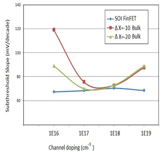 | Figure 4. Effect of channel doping on Subthreshold Slope of pie gate Bulk FinFET and SOI FinFET |
3.2. Pie Gate Bulk FinFET with Punch through Stopper
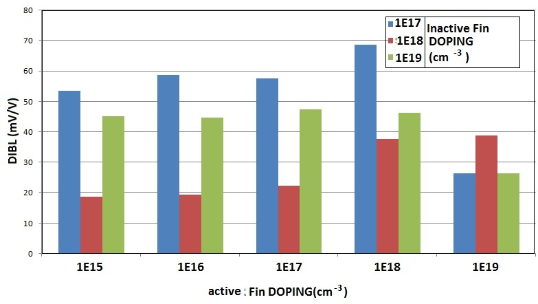
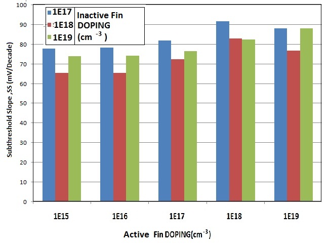
- In this section of work, bulk FinFET with heavy body doping (punch through stopper doping)[9] is studied. We doped pie gate FinFET with punchthrough stopper doping and characterized the performance. The heavy body doping bulk FinFET is simulated for ∆Xj=0nm, ∆Xj=-10nm & ∆Xj=-20nm. For ∆Xj=-10nm, SS is 70.62 mV/decade and DIBL is 28mV/V. For ∆Xj=-20nm, SS is 60 mV/decade and DIBL is 25.6 mV/decade. It is clear that performance of device is significantly improved than previously reported profile and also its value is compared with SOI FinFET(Fig. 4). A graph of DIBL and Subthreshold slope is plotted for different bulk structures and has been shown in Fig. 5 & 6. The subthreshold performance is also studied with variation in channel doping with different Fin structures(Fig. 3). It is observed that device with heavy bulk doping with misalignment ∆X=-20nm has subthreshold performance almost similar to the SOI FinFET.
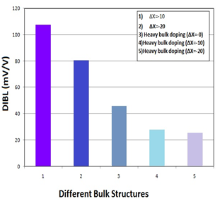 | Figure 5. DIBL Characteristics for different bulk FinFET structures |
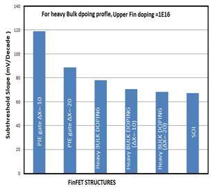 | Figure 6. Subthreshold slope for different Bulk FinFET Structures |
3.3. Bulk FinFET with Bottom Spacer
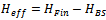
- Bulk FinFET with bottom spacer is shown in Fig.3. Height of bottom spacer is 30nm, so effective Fin height become 30nm (HFin-HBS), where HFin is height of actual Fin and HBS is height of bottom spacer. This reported structure has initially analysed for uniform channel doping profiles and non-uniform doping profiles.
3.3.1. Bottom Spacer with Uniform Channel Doping Profile
- In uniform Bulk doping, active Fin & inactive Fin doping are same. Simulation is done using different Bulk doping. The results are shown in Fig. 7. Similar to the Bulk structure, this device also need high channel doping to control SCEs. The performance of device is better with high channel doping than low channel doping but it is not satisfactory .
 | Figure 7. Bulk FinFET with uniform channel doping |
3.3.2. Bottom Spacer with Non-uniform Channel Doping Profile
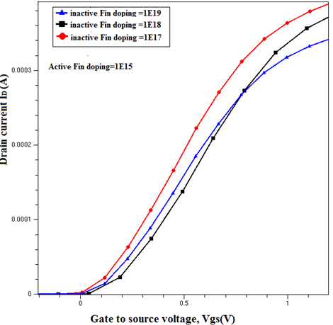
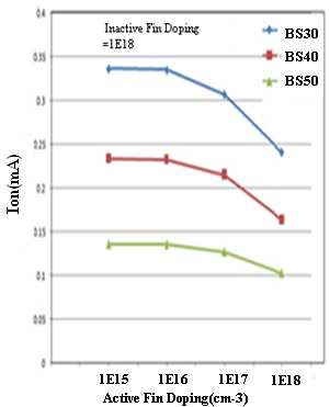
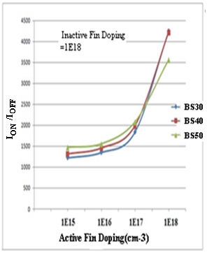
- The Bottom spacer with uniform bulk doping is not satisfactory. It needs higher channel doping for high performance and our aim is to optimize bulk FinFET, so that we get high performance with low channel doping. Here we have used different channel doping in active and inactive Fin regions. Simulations are carried out for two purposes i) Optimization of inactive Fin doping ii) Optimization of active Fin doping.i) Optimization of inactive Fin doping: For optimization of inactive fin doping, simulation is performed for different inactive fin doping keeping active fin doping constant. Different performance parameters have been measured. It is clear that high lo Figure 9 shows the relation between OFF state current and inactive channel doping. The ON/OFF Current is also measured for different active Fin doping. High doping results in low OFF state current but very high (i.e. 1E19) band to band tunnelling and causes degradation in performance. For very high inactive Fin doping OFF current is higher, so proper optimization of doping profile is required to get best performance. Graph of Figure 10 shows ION/IOFF for different inactive Fin Doping.wer Fin doping gives better performance than low lower Fin doping because for high doping there will be lesser influence of drain electric field and it also lowers the junction leakage current. Graph of ON state current for different inactive channel doping is shown in Fig(8). The ON state current is decreasing with increasing inactive channel doping.
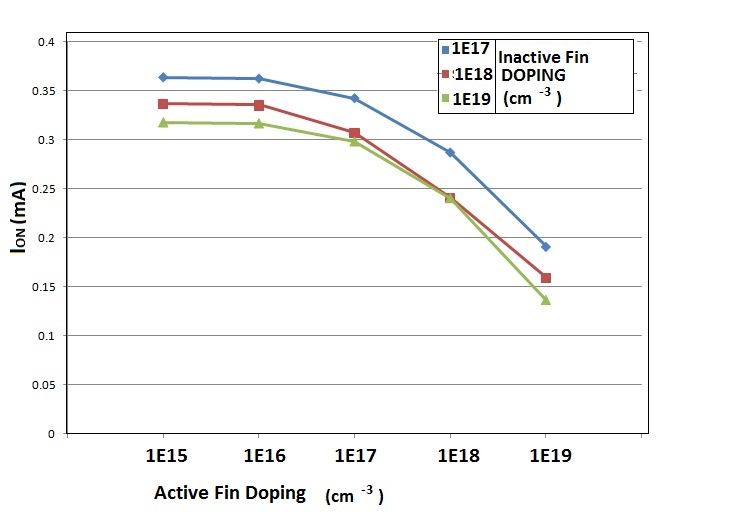 | Figure 8. ION for different inactive channel doping |
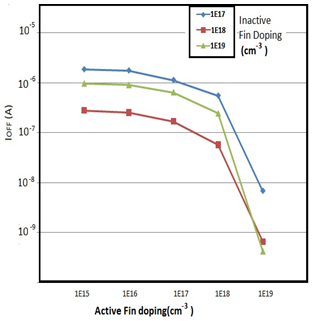 | Figure 9. IOFF for different inactive channel doping |
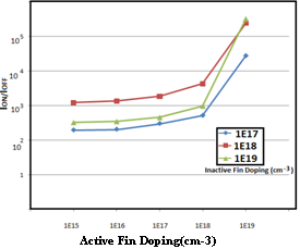 | Figure 10. ION/IOFF for different inactive channel doping |
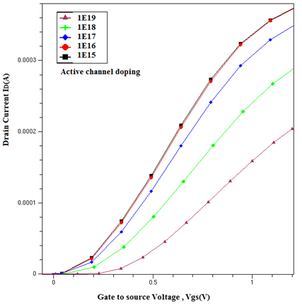 | Figure 11. Transfer Characteristic of Bottom spacer Bulk FinFET For different active Fin Doping(keeping inactive Fin doping constant) |
 | Figure 12. Transfer Characteristics of Bulk FinFET with different inactive Fin doping (Active Fin doping constant) |
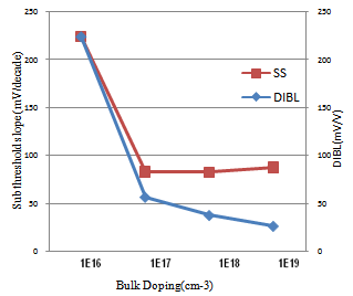
 | Figure 13. DIBL Vs Upper Fin Doping |
 | Figure 14. SS Vs Upper Fin Doping |
 | (2) |
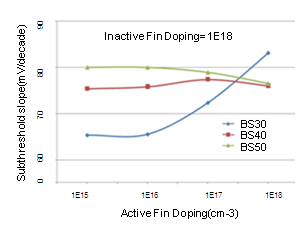
 is total Fin height. Hence from equation (1) and (2) the effective channel width of device reduces with bottom spacer height and therefore reduces the ON current with increasing bottom spacer. Unlike SOI FinFET with bottom spacer DIBL in bulk FinFET reduces with increasing bottom spacer height (Figure 15) and subthreshold performance degrades with spacer height (Fig. 16). But the performance becomes less dependent on active Fin doping for high bottom spacer height.
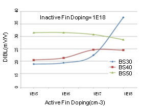 | Figure 15. DIBL on different bottom spacer height |
 | Figure 16. Subthreshold slope for different bottom spacer height |
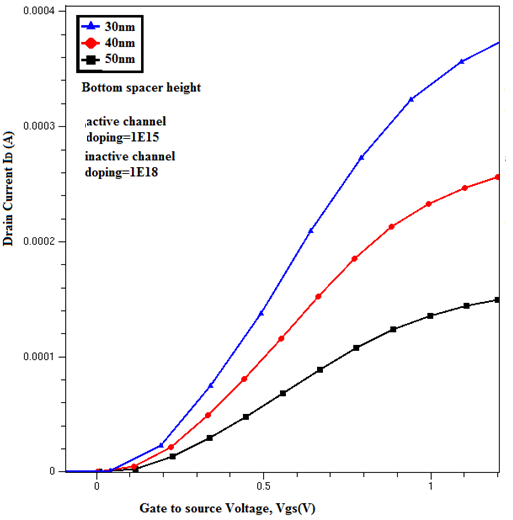 | Figure 17. Transfer Characteristic for Different bottom spacer height |
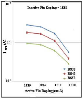 | Figure 18. IOFF for different bottom spacer height |
 | Figure 19. ION for different bottom spacer height |
 | Figure 20. ION/OFF for different bottom spacer height |
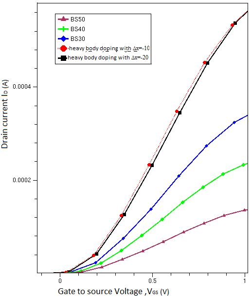 | Figure 21. Transfer characteristics of different FinFET structures |
4. Conclusions
- In first part of results, the novel proposed pie-gate Bulk FinFET (misalignment ΔXj negative) with heavy body doping (Punchthrough stopper) proved better as compared to results in previous bulk FinFET structures. The bulk FinFET designed with Bottom spacer (height: 30nm) and non-uniform Fin doping(i.e. high inactive Fin doping and low active Fin doping) which is equivalent to pie-gate FinFET with punchthrough stopper, shows improved subthreshold performance and it has lesser fabrication complexity. The subthreshold performance is also compared with increasing height of Bottom Spacer (30nm, 40nm & 50nm). It is observed that Performance degrade with increasing height of bottom spacer but the dependency over active channel doping decreases. This shows that it become independent of process variations caused by impurity concentration densities which can be considered as the biggest advantage of bottom spacer structure. Therefore, to exploit above advantage we should keep the optimized value of spacer height while keeping ON state performance well above the ITRS standards.