Keerti Kumar. K, Bheema Rao. N
Department of Electronics & Communication Engineering, National Institute of Technology Warangal, Warangal, 506004, A.P, India
Correspondence to: Keerti Kumar. K, Department of Electronics & Communication Engineering, National Institute of Technology Warangal, Warangal, 506004, A.P, India.
| Email: |  |
Copyright © 2012 Scientific & Academic Publishing. All Rights Reserved.
Abstract
In the deep sub-micron regime it is very critical to deal with the sub-threshold leakage currents. At different levels of abstraction in chip design, this current constitutes more than fifty percent of the total leakage current. In this paper a method for reducing sub-threshold leakage which uses Variable Gate Oxide Thickness MOSFET as an alternate to the high threshold voltage device is proposed. An inverter and a two-input NAND gate which uses VGOT MOSFET are simulated using LT-SPICE. The simulation results show a betterment of 77% and 32.32% in sub-threshold leakage reduction for inverter and two-input NAND gate respectively when compared with the sub-threshold leakage current of the circuits which used no leakage reduction mechanism. The simulation results also show an improvement of 50.64% and 15.15% leakage reduction for inverter and two-input NAND gate respectively when compared with the conventional high threshold voltage MOSFET circuits.
Keywords:
Variable Gate Oxide Thickness MOSFET, Sub-threshold Leakage Current, Oxide thickness, Threshold Voltage, Weak Inversion Current
Cite this paper: Keerti Kumar. K, Bheema Rao. N, Sub-threshold Leakage Current Reduction Using Variable Gate Oxide Thickness (VGOT) MOSFET, Microelectronics and Solid State Electronics , Vol. 2 No. 2, 2013, pp. 24-28. doi: 10.5923/j.msse.20130202.02.
1. Introduction
The demand for low power designs has grown vastly in the last two decades due to tremendous increase in demand of portable and handheld battery operated devices. As the technology is getting scaled into the nanometer regime, the sub-threshold leakage current increases exponentially due to scaling down of parameters like threshold voltage, oxide thickness etc., resulting in short-channel effects[1]. Hence static power dissipation becomes more dominant than dynamic power dissipation. Short-channel MOS transistor devices have channel length of the same order of magnitude as the depletion region thicknesses of the source and drain junctions or approximately equal to the source and drain junction depth.In small geometry MOS transistors, the current flow in the channel depends on creating and sustaining an inversion layer on the surface. If the gate bias voltage is not sufficient to invert the surface, i.e., Vgs < Vth the carriers (electrons) in the channel face a potential barrier that blocks the flow of carriers from source to drain due to weak inversion[2],[3].As the gate voltage increases, the potential barrier decreases, leading to an increase in the flow of carriers due to strong inversion under the influence of the channel electric field. This simple picture becomes more complicated in small-geometry MOSFETs (Metal Oxide Semiconductor Field Effect Transistor), because the reduction of the potential barrier eventually allows electron flow between the source and the drain, even if the gate-to-source voltage is lower than the threshold voltage (Vth). 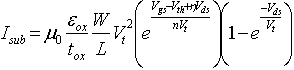 | (1) |
The channel current that flows under these conditions (Vgs < Vth) is called the weak inversion or sub-threshold current Isub. Leakage power is combination of many other current components such as channel edge current, Drain Induced Barrier Lowering (DIBL) current and weak inversion current. The weak inversion currents are inversely proportional to the gate oxide thickness and exponentially dependent on threshold voltage given by equation (1). In stand-by mode the power dissipation is dominant due to sub-threshold leakage current because the functional and short-circuit currents are non-existent[4],[5].In equation (1) Isub is the sub-threshold current, W, L are the width and length of the transistor,  is the carrier mobility, Vt is the thermal voltage,
  is the DIBL coefficient, n is the sub-threshold swing, Vds is the drain to source voltage, Vgs is the gate to source voltage, Vth is the threshold voltage,
  is the permittivity of the oxide, tox is the thickness of the oxide.A transistor level approach for reducing sub-threshold leakage current has been reported in[6],[7]. The thickness of the oxide in the MOSFET has been varied uniformly[6] and non-uniformly[7], the device thus obtained is a Variable gate oxide thickness MOSFET. These devices when used as sleep transistors have led to significant reduction in the weak inversion current.This paper uses the transistor level approach reported in[6],[7] into circuits and the transistor model is used as alternate to the conventional high threshold voltage MOSFETs which are more used for leakage minimization. This transistor model (explained in section 2) eliminates the complex and costly fabrication process steps involved in the fabrication of conventional high threshold voltage MOSFETs. The fabrication of this transistor requires only few process steps in addition to the process steps of a normal MOSFET. The structure of the VGOT MOSFET has been explained in section.2, the usage of VGOT MOSFET in circuits such as inverter and a two input NAND gate has been explained in section.3. Section.4 elaborated the results of the inverter and the two input NAND gate and in section.5 conclusions were made and future scope of the work is suggested.
2. Variable Gate Oxide Thickness (VGOT) MOSFET
The structure of VGOT MOSFET shown in Figure.1 consists of stacked gates G1, G2 and G3. The input and the transfer characteristics of the VGOT MOSFET reported in[6],[7] are briefly described. As with the conventional MOSFET operation, when the MOSFET is subjected to the drain voltage bias and the gate voltage bias such that Vgs < Vth weak channel inversion occurs. The operation is similar to the normal MOSFET with gate G1. With Gate G2 the sub-threshold current is lower to that of the sub-threshold current of G1 and higher when compared with the sub-threshold current using G3 as the gate terminal. This is the direct consequence of the rise in threshold voltage of the transistor as the oxide thickness increases. 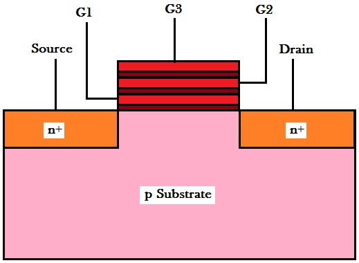 | Figure 1. Variable gate oxide thickness MOSFET |
3. Circuit Implementation
An implementation of a logic circuit with VGOT MOSFET as a sleep transistor is shown in Figure.2. A sleep transistor cuts off the path from supply to ground when the logic circuit is off. Thus the gates G1, G2 and G3 of VGOT MOSFET (Figure.2) are operated such that the leakage current is minimized.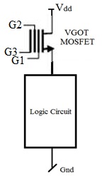 | Figure 2. A Logic circuit with a VGOT MOSFET as sleep transistor (instead of a high Vth transistor) |
In most of the system designs it is observed that always seventy percent of the circuits are found in standby mode (either ON or OFF) which constitutes static current. If a particular OFF circuit is to be made inactive it should be made in such a way that its effect is not felt on the other parts of the circuit. In an inactive circuit the leakage current is most often found to be the weak inversion current[4].If a small circuit constitutes to the leakage, then in a system design, each of the inactive parts constitute to more leakage current. Most often the components which are inactive constitutes the overall leakage current of the system. In this situation a mechanism is needed which makes the weak inversion current very negligible or reduced to some extent.
3.1. Inverter
Figure.3 shows the implementation of an inverter with VGOT MOSFET, M3 as the sleep transistor and the transistors M1 and M2 form a normal inverter. As the technology model for a VGOT MOSFET is not modelled in LT-SPICE (Linear Technology-Simulation Program for Integrated Circuits Emphasis), the gate oxide thickness of the transistor M3 is varied. The oxide thicknesses of transistor M3 are chosen to be higher than the oxide thicknesses of transistor M1 and M2. The oxide thickness of transistor M3 is varied in accordance with the values in the technology allowable range. An inverter is implemented with 90nm technology and simulated in LT-SPICE.The oxide thickness tox of the VGOT MOSFET is varied in three iterations. In the first iteration the oxide thickness is varied as if the gate G1 of VGOT MOSFET is biased. Whenever the inverter is operated in active mode, the transistor M3 is turned on by biasing the gate G1 and the inverter works normally. In the second iteration tox is slightly increased as if gate G2 of the device has to be biased. In a situation if the functionality of the inverter is not required for a specific operation, then the inverter can be operated in the standby mode by biasing the gate G2 of the VGOT MOSFET appropriately. This directly depicts the relationship between the threshold voltage and the gate oxide thickness of MOSFET. The threshold voltage of the MOSFET is a function of tox, which states that the threshold voltage of the device is increased if oxide thickness is increased. This makes the inverter isolated from the supply voltage. So this offers a low weak inversion current, as the gate of the VGOT MOSFET is still biased. In the third iteration of tox is further increased as if gate G3 of VGOT MOSFET is to be biased. If more reduction in weak inversion current is expected then the gate G3 is biased, it offers very less weak inversion current than the current measured when the gate G2 is biased. The overall weak inversion current measured for the circuit is lesser when the terminals G2 and G3 are biased.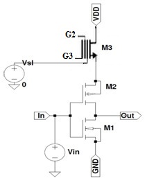 | Figure 3. An Inverter with a VGOT MOSFET as sleep transistor |
3.2. A Two-Input NAND Gate
As another logic circuit with VGOT MOSFET as a sleep transistor, a two input NAND gate has been implemented and the performance of VGOT MOSFET in reducing the sub-threshold current is studied. Figure.4 shows the implementation of a two input NAND gate where the transistors M1, M2, M3 and M4 combine to form a CMOS (Complementary Metal Oxide Semi -conductor) NAND gate and the transistor M5 is the VGOT MOSFET acting as a sleep transistor. As the technology used is 90nm technology, the threshold voltage of the transistors in the CMOS NAND gate is 0.18V and the supply voltage is 1.2V[8]. If the input voltages are higher than this threshold value the gate works normally provided transistor M5 is turned ON. If the inputs are lesser than Vth of the NAND gate transistors the current flowing through the circuit is sub-threshold current, in which case the sleep transistor has to be switched OFF and the logic circuit is disconnected from the supply voltage.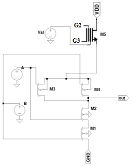 | Figure 4. A two input NAND gate with a VGOT MOSFET as sleep transistor |
4. Results
4.1. Inverter
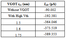
As stated in section 3.1 the inverter is implemented in 90nm technology and simulation results for sub-threshold current with and without VGOT MOSFET are obtained. Table.1 shows the value of weak inversion current and correspondingly the current is plotted against variation of oxide thickness in Figure.5. The weak inversion current measured for the inverter circuit without using the VGOT MOSFET is -90.002pA and it is -192.381pA using a conventional high threshold voltage transistor. Point A and point B in Figure.5 corresponds to the weak inversion current without using VGOT MOSFET and using a conventional high threshold voltage transistor respectively.Table 1. tox vs Isub for Inverter
 |
| |
|
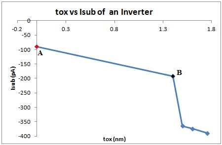 | Figure 5. Physical gate oxide thickness vs sub-threshold current of an Inverter |
The curve below point B is plotted between sub-threshold current and oxide thickness as a parameter. If the inverter is biased with a voltage slightly lesser than the threshold voltage of the nMOS (M1) or pMOS (M2) transistor of the inverter the current which flows through the shorted drain terminals of nMOS (M1) and pMOS (M2) transistors is equal to the sub-threshold current through the inverter. The weak inversion current measured when gate G1 is used is found to be -364.046pA. In the second iteration the physical gate oxide thickness parameter in the technology model file of M3 is made higher than the value chosen in the iteration1. The weak inversion current measured at this point, measured to be -373.519pA, and is lesser compared to that measured in the iteration1. In the third iteration the physical gate oxide thickness parameter in the technology model file of M3 is made higher than the value chosen in the iteration2. The weak inversion current is measured at this point, measured to be -389.353pA, and is lesser compared to that measured in the iteration2.From Table.1 it can be inferred that for every 0.1nm increase in gate oxide thickness the sub-threshold current falls 10pA for an inverter when VGOT MOSFET is used as a sleep transistor.
4.2. Two input NAND gate
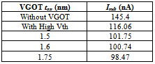
Table 2. tox vs Isub for a 2 input NAND gate
 |
| |
|
As stated in section 3.2 a two input NAND gate is implemented and simulated. Table.2 shows the simulation results for the sub-threshold current and Figure.6 shows the plot of sub-threshold current for a two input NAND gate against gate oxide thickness. As found with the inverter point A and point B in Figure.6 corresponds to the weak inversion current without VGOT MOSFET and with conventional high threshold voltage MOSFET respectively. The curve below the point B in Figure.6 is in accordance with the curve below the point B in Figure.5. But in a two input NAND gate for every 0.1nm rise in oxide thickness the sub-threshold current falls by 1nA.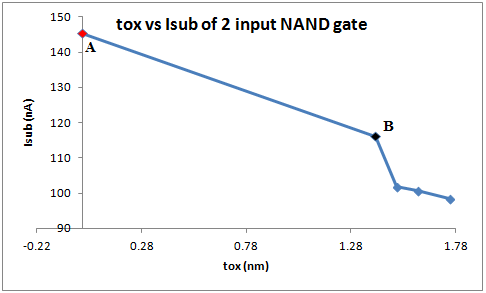 | Figure 6. Physical gate oxide thickness vs sub-threshold current of a 2 input NAND gate |
5. Conclusions
An alternative to the high threshold voltage transistor is proposed in this paper. The technology of using VGOT MOSFET eliminates the need of many critical and costly process steps which were inherent in the fabrication of high threshold voltage transistors. Apart from the difficulty faced in the fabrication steps of high threshold voltage device, VGOT MOSFET is also proved to be a better solution in terms of leakage power reduction. We have implemented an inverter and two input NAND gate using VGOT MOSFET as a sleep transistor. From the simulation results we compare the leakage current reduction in three aspects. Firstly, we found an improvement of 77% and 32.32% in sub-threshold leakage reduction for inverter and two-input NAND gate respectively when compared with the circuits which have not used any sleep transistor in their operation. Secondly, the simulation results show an improvement of 50.64% and 15.15% leakage reduction for inverter and two-input NAND gate respectively when compared with the conventional high threshold voltage MOSFET circuits. Finally, we infer that for every 0.1nm increase in oxide thickness the sub-threshold current falls by 10pA and 1nA for inverter and two input NAND gate respectively. A similar circuit topology can be implemented with complex logic circuits and can be used for system designs where longer battery time for battery operated hand held devices has to be assured.
References
| [1] | Raychowdhury, A. Paul, B.C. Bhunia, S. Roy, K. "Computing with sub-threshold leakage: device/circuit / architecture co-design for ultralow-power sub-threshold operation," Very Large Scale Integration (VLSI) Systems, IEEE Transactions on, vol.13, no.11, pp.1213-1224, Nov. 2005. |
| [2] | Sung-Mo Kang, Yusuf Leblebici, “CMOS Digital Integrated Circuits analysis and design”, Third edition Tata McGraw-Hill Edition 2003. |
| [3] | Jan M Rabaey, Anantha Chandrakasan, Borivoje Nikolic, “Digital Integrated Circuits A Design Perspective”, Second Edition, PHI 2003. |
| [4] | P.R.van der meer, A.van Stavaren and A.H.N van Roermund, “Low power deep submicron CMOS logic sub threshold current reduction”, Springer 2004. |
| [5] | Siva G Narendra, Anantha Chandrakasan, “Leakage in nanometer CMOS Technologies”, Springer 2006. |
| [6] | K.Keerti Kumar, N.Bheema Rao, “Variable Gate Oxide Thickness MOSFET: A Device level solution sub-threshold leakage current reduction”, Proc. of 2012 Intl conference on Devices, Circuits and Systems. |
| [7] | K.Keerti Kumar, N.Bheema Rao, “Characterization of Variable gate oxide thickness MOSFET with non uniform oxide thicknesses for sub-threshold leakage reduction”, Proc. of 2012 International conference on Solid state and Integrated Circuit (ICSIC 2012). |
| [8] | BSIM 4.3.0 MOSFET Model – User’s Manual |
 Abstract
 Reference
 Full-Text PDF
 Full-text HTML