-
Paper Information
- Paper Submission
-
Journal Information
- About This Journal
- Editorial Board
- Current Issue
- Archive
- Author Guidelines
- Contact Us
Microelectronics and Solid State Electronics
p-ISSN: 2324-643X e-ISSN: 2324-6456
2013; 2(2): 11-23
doi:10.5923/j.msse.20130202.01
Design of Field-programmable Operational Transresistance Amplifier using Floating-gate MOSFETs
 Abstract
 Reference
 Full-Text PDF
 Full-text HTML
Garima Kapur1, Sajal Mittal2, CMMarkan1, VPPyara3
1Department of Physics & Computer Science, Dayalbagh Educational Institute, Agra, 282005, India
2Department of Electrical engineering, Indian Institute of Engineering, Kanpur, India
3Department of Electrical Engineering, Dayalbagh Educational Institute, Agra, 282005, India
Correspondence to: Garima Kapur, Department of Physics & Computer Science, Dayalbagh Educational Institute, Agra, 282005, India.
| Email: |  |
Copyright © 2012 Scientific & Academic Publishing. All Rights Reserved.
We propose a comprehensive design procedure to design Field-programmable/Reconfigurable Analog Integrated CMOS circuits. Instead of repeatedly iterative simulation steps to achieve desired design specifications by fine tuning the W/L ratios of the FETs, we use first order classroom equations to achieve central value of desired specifications and then execute a customized fine tuning of specifications to the customers requirement with the help of Floating-gate Transistors FGMOS. To demonstrate the proposed design cycle, a modified high frequency/RF Operational Transresistance Amplifier (OTRA) CMOS circuit is designed where transresistance gain and input output low impedances are programmable, independently to desired values within a specific field range, using FGMOSs. In FGMOS the programmable charge at floating-gate using external voltages can results in threshold voltage field-programming, which in turn program the design (OTRA) specifications. With specific sizing and biasing condition, the transresistance can be programmed from 0.5kohm to 6kohm, input and output impedance from 600ohm to 10Kohm, while offset current can also be compensated independently using respective FGMOSs with 13-bit programming precision. However the final circuit, with four FGMOS occupies 75µm × 64µm chip area. The design also consumes less power, total power consumption is about 3.96mW and show good thermal stability as output voltage variation with temperature is about 25µV/°C.
Keywords: Floating-gates, Field Programmable Analog Array, Operational Transresistance Amplifier, Specifications, Threshold Voltage
Cite this paper: Garima Kapur, Sajal Mittal, CMMarkan, VPPyara, Design of Field-programmable Operational Transresistance Amplifier using Floating-gate MOSFETs, Microelectronics and Solid State Electronics , Vol. 2 No. 2, 2013, pp. 11-23. doi: 10.5923/j.msse.20130202.01.
Article Outline
1. Introduction
- The growing demand for mobile communications has led to high level of chip integration and directed research towards the field of high frequency applications. In the new designed circuit topologies for high frequency signal processing conventional methods based on voltage op-amp are no longer adequate as op-amp has a closed-loop gain dependent bandwidth, thus current-mode approach is preferred. Current mode circuits has potential advantages over their voltage counterparts, such as their inherently wide bandwidth, higher slew-rate, greater linearity, wider dynamic range, simple circuitry and low power consumption[1] and hence suitable for high frequency operations. In 1985 the popularity of current feedback op-amp amplifiers (CFOA) has increased considerably as they were found to be able to overcome the limitations arising from conventional operational amplifiers[2]. The term current-feedback is used because the error signal entering at the feedback node of the op-amp is in the form of a current and this gives to the amplifier a constant closed loop bandwidth capability[3]. Since the CFOA has a larger bandwidth and a higher slew-rate than the conventional op-amp, analog signal processing circuits built around the CFOA are expected to operate at higher frequencies than the op-amp based circuits[4]. An alternate current-mode circuit, operational transresistance amplifier (OTRA), is a three terminal analog building block shown symbolically in Figure 1(b) and defined using matrix, shown in Figure 1(b)[5]. It has similar transmission properties to the current-feedback op-amp, with an addition of two low-impedance inputs and one low-impedance output. OTRA, which is commercially available under the name of Norton amplifier (like Z10040A Norton noiseless feedback Amplifier[6]) have been attracted attention by its advantages in the current-mode circuit design. These commercial realizations do not provide a true virtual ground at the input terminals and they allow the input current to flow in one direction only. The former disadvantage limited the functionality of the OTRA whereas the latter forced to use external dc bias current leading complex and unattractive designs[7]. In order to remove these disadvantages of the OTRA, some topologies are proposed in the literature[8-10]. But these solutions are both complex structures and they do not operate properly at low power supplies, however in future design concept the main interest is designing circuitries with low power supplies. This demand leads designing a high performance CMOS differential OTRA for the current-mode analog systems design[11-14]. In CMOS OTRA design both the input and output terminals are characterized by low impedance. The input terminals are virtually grounded leading to circuits that are insensitive to stray capacitances[5]. Ideally the transresistance gain, Mr., approaches infinity, and applying external negative feedback will force the two input currents I+ and I−, to be equal (see Figure 1). This leads to growing interest for the design of OTRA-based analog signal processing circuits, such as instrumentation amplifiers MOSFET-C differentiator, integrators, continuous-time filters, immitance simulators, waveform generators, bistable multivibrators, oscillators[15-24]. A low-pass, band-pass, high-pass, and band-reject biquad filter is proposed using two OTRAs, three capacitors, and several resistors[19]. The phase shifter uses n-OTRA is tunable and blocks to give a total of n+1 oscillation[20]. A voltage-mode proportional-derivative using single OTRA, two resistors and a capacitor, having orthogonally tunable proportional and derivative constants[25] is proposed. Similarly a single OTRA with a capacitor and five resistors are used to propose a grounded negative inductance emulator with full independent control on both the inductance value and the condition[10]. These circuits require additional circuitry to introduce tuning ability within them. Thus programmable devices are required for accurate prototyping/on-chip tuning ability of the design. These circuits also experience limitation in applications like in highly integrated portable electronic devices, where less power consumption and small size hardware with higher integration is required. Moreover, there are various electronic systems where high precision tuning ability/programmability is required like for biologically inspired circuits such as bionic ear processor, learning circuits and related adaptive filters, neuromorphic and cellular computing circuits, etc. Instead of using additional circuitry we would like to modify the basic OTRA CMOS circuit[5] using Floating-gate Transistors (FGMOS) in place of conventional MOS, to introduce non-volatile, high precision on-chip programming in the OTRA design.
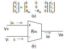 | Figure 1. (a) I-V Describing matrix of OTRA (b) Schematic Diagram of OTRA |
2. Proposed Analog Design Cycle
- Although vigorous development of consumer electronic products has been propelled by advancements in digital processing technology, the world is still analog. Sound, video and image are always represented in the form of analog signals. Analog designs tend to have higher integration density, consume less power and interface easily with the real world yet they are still less preferred option compared to their digital counterparts as analog implementation lacks accurate convertibility of design to prototype, stability of devices, long term storage of analog signals, field programmability and automated design. Analog design is more concerned with the physics of the semiconductor devices such as gain, matching, power dissipation, and resistance. However, fidelity of analog signal amplification and filtering is usually critical and as a result, analog IC design is critical. Thus there is a drive towards shorter design cycles for analog integrated circuits, which demand the development of high performance analog circuits that are reconfigurable and suitable for CAD methodologies[34]. Several manufactures have made programmable analog circuits; among these are Motorola, IPM Inc, Lattice and Anadigm. Several designs of Field Programmable Analog Arrays (FPAA) have been reported[35]-[38], but these are often aimed at a commercial market as an analog counterpart to Field Programmable Gate Arrays (FPGA) for rapid prototyping of analog circuits. Subsequently to introduce programmability in analog designs programmable device are also developed such as various methods are developed to modify electrical characteristics of MOS device which in turn introduce programming ability in MOS. It is performed either through openings in the passivation layer to define location of bonding pad or through ion implantation at exposed underlying polysilicon gate structure which create an implantation layer at the channel regions of selected MOS devices, and thereby permanently alter the threshold voltages of these MOS devices[39, 40]. However over the last decade there is a new technology based on floating gates have developed and floating gate circuit approaches have progressed from a few foundational academic results to stable circuits. Floating gate MOS are like conventional MOS with an additional gate in which by modifying the charge at the floating gate MOS characteristics (threshold) can be programmed on-chip after fabrication with real time, non-volatile, reconfigurable programming[41-43]. This programmable analog technology empowers analog signal processing approaches programmable precision analog low-power techniques[44]. Moreover as we move into more advanced CMOS process nodes, it has become apparent to the designers that although the fundamental RF/analog design principles remain unchanged, there have to be new techniques and architectures to fully harness the potential of CMOS scaling and to advance the state of the art. So inspired from floating gate MOS technology, we would like to propose a paradigm shift in analog circuit designing where instead of repeatedly iterative simulation steps to achieve very precise design specifications by fine tuning the W/L ratios of the FETs, we use first order classroom equations to achieve central value of desired specifications and then execute a customized fine tuning of specifications to the customers requirement. The proposed analog design cycle flowchart and algorithm is illustrated in Figure 2. As conventional Analog design cycle consists of basic five steps: system modelling, circuit simulation, layout, physical verification and post layout verification i.e. it is useful to first model the behaviour of those system to understand its stability condition and system response, then for targeted specifications some changes such as architectural change in circuit, resizing of transistors might be needed. This can be achieved by manual design, table-based calculation employing Excel or Matlab, circuit sizing by Genetic Algorithms or Particle-Swarm- Optimization or by circuit simulations like SPICE. However, troubleshooting of each step is very complicated. It is a loop linked back to the previous steps and possibly troubleshooting all the way back to step1. However our approach towards circuit design is different because with the help of post fabrication programmability feature in FGMOSs, desired specification values can be adjusted by a field user Algorithm:1. Analyse circuit with the help of block diagram to establish desired functionality.2. Simulate the circuit to check its functionality with basic sizing and biasing conditions.3. Design the equivalent small-signal model of the circuit.4. Derive specifications in terms of threshold voltage of transistors.5. Analyse sensitivity of each specification with respect to respective thresholds.6. Simulate the circuit to check the sensitivity of each specification.7. Layout creation and verification of the circuit with basic sizing and biasing conditions. Then after testing and extraction, fabricate the design.8. Program the transistor’s thresholds to adjust the desired specifications with huge accuracy
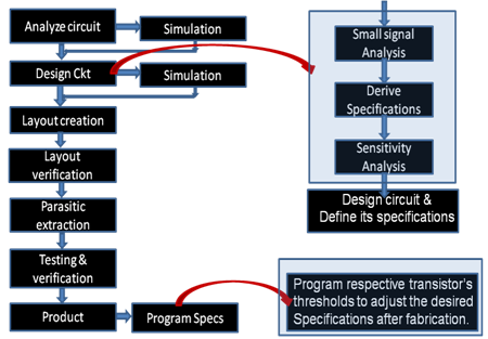 | Figure 2. Flowchart of Proposed Analog IC Design Procedure |
2.1. Design Objectives
- Before designing or introducing programmability in OTRA CMOS circuit few design objectives need to be considered. Firstly the variation in the design specifications should be large and continuous. Indirect, non-volatile and high precision programming of FGMOS thresholds can produce large range and continuous programming of specifications. However, large continuous variation in specifications is difficult and sometimes unstable. Second design objective is that the variation of each specification should be independent of the other i.e., each specification should be programmed either by one or more FGMOS but should not alter any other design specifications. However if specification programming are not independent then either through modifying the circuit or by compensating the affected specification value using different set of FGMOS, should be prepared. Thirdly, operating point of the circuit should not alter too much during programming, i.e. current density in each transistor should not change significantly or in other words offset current should not vary significantly.
3. Basic CMOS OTRA Design
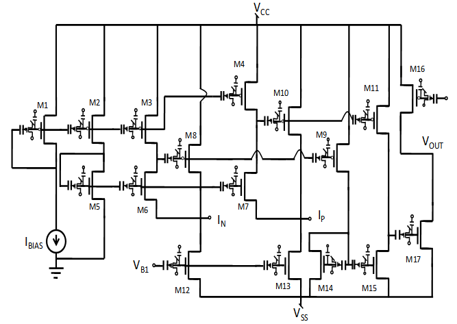
- The OTRA design is a three terminal device whose schematic diagram and its IV describing matrix is shown in Figure. 1. Both the input and output terminals are characterized by low impedance. Ideally the transresistance gain, Rm, approaches infinity and applying external negative feedback will force the two input currents, I+ and I-, to be equal. CMOS OTRA design[5] as shown in Figure 3(a) consists of cascaded connection of the modified differential current conveyor and a common source amplifier.
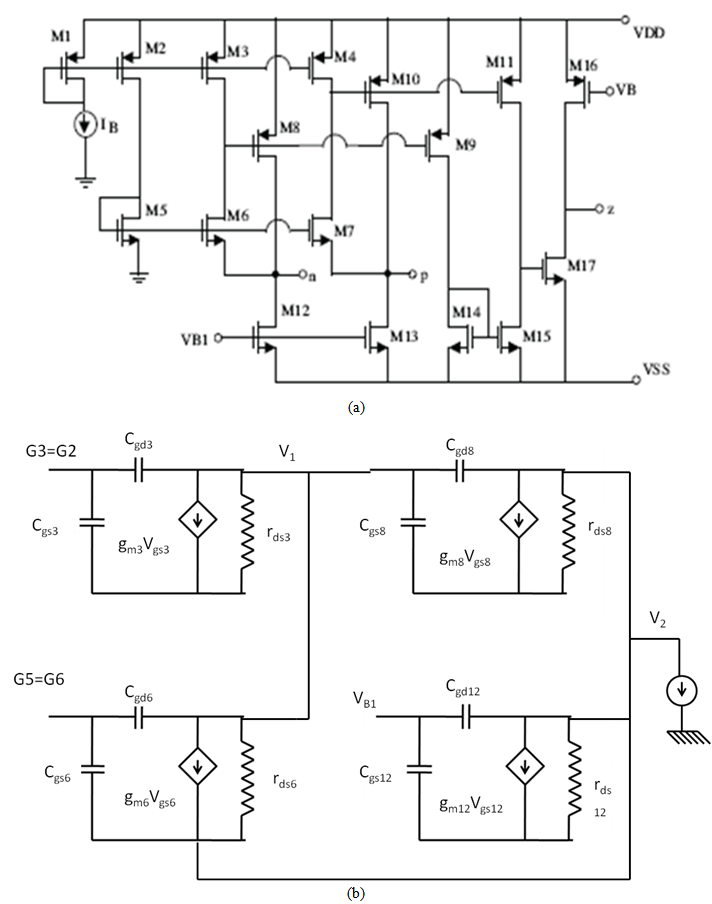 | Figure 3. (a): Circuit diagram of CMOS OTRA[5] (b): High frequency small signal equivalent circuit loop of the OTRA |
3.1. High-frequency Small Signal Analysis
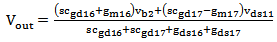
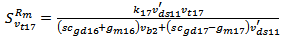
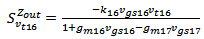
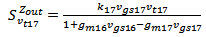
- The OTRA design is operated at high frequency; accordingly high frequency small signal equivalent model is generated and design characteristics are derived. The circuit consists of two loops formed by M3, M6, M8, M9 and M4, M7, M10, M11 which propagates the input current In and Ip respectively. By applying KCL on high frequency small signal equivalent circuit as shown in Figure 3(b), expression for output voltage of OTRA at the output node is derived where current source is I+. The expression of output voltage is evaluated in terms of threshold voltages of MOSs when transconductance is replaced by their corresponding threshold voltages in expression. Hence output voltage can be programmed using threshold voltage of M16 and M17.
 | (1) |
 | (2) |
 | (3) |
 | (4) |
 | (5) |
3.2. Characteristics of Basic OTRA design
- The basic OTRA design has been simulated and its basic functionality with central value of specifications at specific biasing and sizing conditions of the circuit is estimated. Transistors aspect ratio is tabulated in Table1. The biasing current IB = 5μA. The biasing voltages VB = -1 V and VB1 =0.2 V. Thus at a specific sizing and biasing condition of the design, frequency response of transresistance gain magnitude and phase is represented in Figure 4(a) and (b). Figure 4(c) shows the frequency response of the input impendence and figure 4(d) depict temperature stability of the design. The variation in output voltage with changing temperature from -40°C to 80°C is about 25µV/°C. The input differential current range is from -20μA to 20μA. The offset current equals 0.15μA. The input resistance equals 22.139 Ω. The output resistance equal to 12 KΩ. The DC open loop transresistance gain equals 4.054dBΩ (=1.67 KΩ). The gain bandwidth product equals 10.3 GHz Ω. The power dissipation of the circuit equals 9.34mW. The characteristics summary is tabulated in Table2. Hence the characteristic plots of the basic OTRA circuit shows its basic functionality as verified from papers[4-6].
|
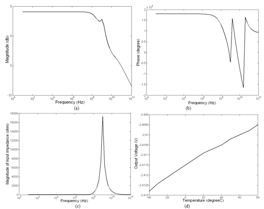 | Figure 4. Frequency Response of (a) Transresistance magnitude (b) Transresistance phase Ip and In (c) Input impedance at port X of OTRA (d) Variation in Output voltage with changing temperature from -40°C to 80°C |
4. Design of Programmable OTRA
- It is observed from simulation results of basic OTRA circuit that the OTRA circuit is justifying its basic characteristics. Now to introduce programmability in this basic OTRA circuit MOSFETs are replaced by floating gate MOSFETs. Floating-gate MOSFETs are conventional MOSFETs wherein memory is stored in the form of charge trapped on floating-gate, affecting its threshold voltage. Two antagonistic quantum mechanical transfer processes, viz. hot e- injection and Fowler Nordheim tunnelling, alter the trapped charge on a floating gate. As these processes can occur during normal operation (indirect programmable using hot e injection and Fowler Nordheim tunnelling simulation model[31, 32]), it leads additional attributes to the FGMOS transistors such as non volatile analog memory storage on floating-gate, locally computed bidirectional memory updates and memory modification during normal transistor operation. It is represented by symbol showing injection and tunnelling nodes, attached at the common floating gate in Figure 5(a).TunnellingCharge is added to the floating gate by removing electron from it by means of Fowler-Nordheim tunnelling across oxide capacitor. This shifts the curve (Figure 5(b)) to the right or in other words threshold voltage of the transistor increases. InjectionCharge is removed from the floating-gate by adding electron on it by impact-ionized hot electron injection from the channel to the floating gate across the thin gate oxide. This shifts the curve (Figure 5(b)) to the left or in other words threshold voltage of the transistor decreases.
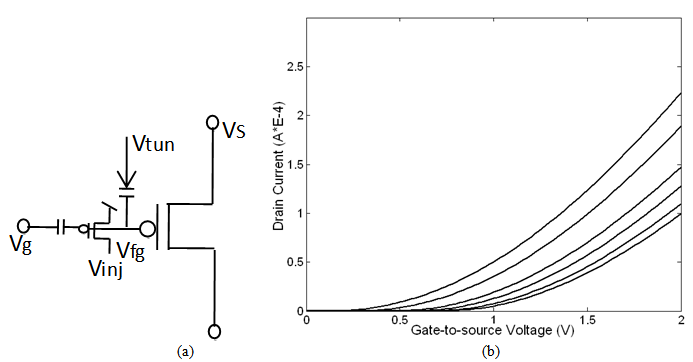 | Figure 5. (a): Pictorial representation of a normal MOS with indirectly programmable floating gate using injection and tunnelling (b) Output Characteristics of a FGMOSFET |
 | Figure 6. Circuit Diagram of proposed modified OTRA design whose specifications are programmable by field user to any desired value |
4.1. Sensitivity Analysis of Design Specifications
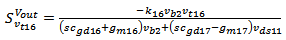
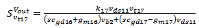
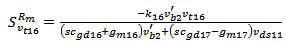
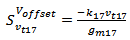
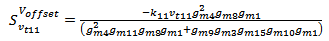
- Output Voltage: - Sensitivity of output voltage Vout has been evaluated using equation (1) which shows dependence on threshold of FGMOSs M16 and M17. Thus the sensitivity of Vout with respect to FGMOSFET M16 is calculated using partial differentiation of Vout w.r.t Vt16 considering rest thresholds constant, is given by:
 | (6) |
 | (7) |
 | (8) |
 | (9) |
 | (10) |
 | (11) |
 | (12) |
 | (13) |
 | (14) |
 | (15) |
 | (16) |
 | (17) |
4.2. Simulation Results Demonstrating Programming Steps to Program Circuit Specifications
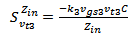
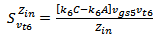
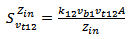
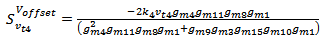
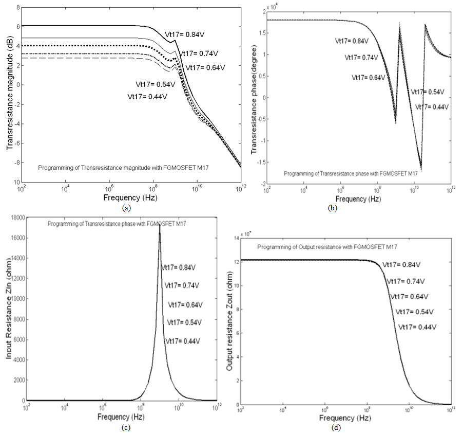
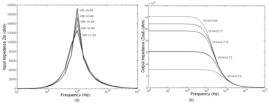
- The circuit diagram of Figure 4 representing modified OTRA design is simulated using BSIM3 level 49 MOSFET models using T-Spice 0.35µm CMOS process and the final circuit with essential number of FGMOS is verified using Cadence analog design tool, Virtuoso. Figure 7 (a)-(d) represent programmable transresistance gain magnitude, phase and input output resistance with respect to threshold of floating gate transistor M17, Vt17. From the plots it is verified that the transresistance magnitude can be programmed independently using threshold voltage of FGMOS M17, Vt17 as rest all specifications input resistance, output resistance even transresistance phase does not vary with Vt17. At particular sizing and biasing condition of the proposed OTRA circuit, the range of transresistance magnitude programming in decibels is from 2 dB to 8dB (= 0.5kohm to 6kohm) where rest all specifications remain constant. Similar variations of each specification with the respect to respective transistor have been performed and dominant FGMOS is identified. Figure 8(a) illustrates programming of input impedance with respect to FGMOS M6 threshold, Vt6. However while programming Vt6, changes occur in the value of transresistance magnitude. In addition to it, Figure 8(b) illustrates programming of output impedance with respect to FGMOS M14 threshold, Vt14. However while programming Vt14, changes occur in the value of transresistance magnitude. Therefore it is observed that each specification shows dependency on more than one FGMOS’s threshold. So with some design modification as well as with iterative simulations each specification can be estimated to be programmed using only one FGMOS threshold, compensating change in rest all other specifications. Thus with iterative simulations and parametric analysis of each specifications, programming steps used to program design specification is tabulated in Table 3. Figure 9 represent parametric analysis results of specifications with respect to respective threshold model parameter, threshold voltage, Vtx. The sensitivity analysis of all specifications w.r.t Vt17 is shown in Figure 9(a). Hence transresistance magnitude Rm can be programmed independently with Vt17, where no change in input, output impedance Zin and Zout and in offset voltage. Figure 9(b) represents that output impedance Zout dominantly vary with threshold of FGMOS M14, Vt14 where transresistance and offset voltage varies significantly, however, input resistance remain constant. Hence transresistance magnitude need to be compensated using FGMOS M17. Similarly sensitivity analysis of all specifications with respect to FGMOS M6 is illustrated in Figure 9(c). It shows that the input impedance Zin varies with threshold voltage of FGMOS M6 where transresistance also varies with M6 however output impedance remains constant. Hence to program input impedance with Vt6, transresistance need to be compensated using FGMOS M17 (Rm is sensitive to Vt17 as shown in Figure 9(a)). Therefore, the final modified circuit consists of four FGMOS which can program transresistance, input impedance, output impedance and offset voltage to any desired value within the defined range with very high precision.(about 13 bit programming resolution is observed and the same programming precision is claimed in paper[33]). Thus the final circuit consists of four FGMOSs and its circuit diagram and layout are shown in Figure 10(a) and (b). In addition to it, the programming steps which demonstrate the range and method to program circuit specifications is tabulated in Table3. The final OTRA design with help of four indirectly non-volatile field-programmable FGMOS, can program its design specifications along with offset output voltage with high accuracy, as illustrated in next section.
 | Figure 7. (a) Variation of Transresistance magnitude in dB with programmable thresholds of FGMOS M17 Vt17 (b) Variation of Transresistance phase in degree with programmable thresholds of FGMOS M17 Vt17 (c) Variation of input impedance Zin (ohm) with programmable threshold of FGMOS M17 Vt17 (d) Variation of output impedance Zout (ohm) with programmable threshold of FGMOS M17 Vt17 |
 | Figure 8. (a) Variation of input impedance Zin (ohm) with programmable threshold of FGMOS M6 Vt6 (b) Variation of input impedance Zout with programmable threshold of FGMOS M14 Vt14 |
 | Figure 9. (a): The sensitivity analysis of all specifications w.r.t Vt17 (b): The sensitivity analysis of all specifications w.r.t Vt14 (c) The sensitivity analysis of all specifications w.r.t Vt6 |
|
4.3. Final OTRA Circuit with Required Floating Gate Transistors and its Programming Steps
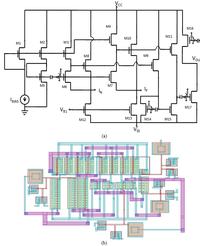 | Figure 10. (a) Schematic of final modified Field Programmable High frequency OTRA developed using BSIM 3 level 49 models in Virtuoso (Cadence analog designer tool) 0.35µm CMOS process using only four FGMOSs. (b) Layout of final OTRA circuit in which transresistance, input output impedance and offset voltage can be programmed independently using FGMOSs (M17, M14 and M6 respectively), which in turn can be programmed using two pFETs (mos capacitor for tunnelling and programmer PMOS for injection) at common floating gate, using external control voltages Vtun and Vinj, whereas, the charge at the floating gate can be stored at capacitor (160pF), placed between gate and floating gate of the floating gate transistor |
- The final modified programmable OTRA circuit using only three floating gate transistors M17, M6 and M14, is simulated using BSIM3 level 49 MOSFETs model along indirectly programmable FGMOS’s simulation model using Virtuoso, 0.35 um CMOS process, as shown in Figure 10(a). The design is also being developed for fabrication and the layout is demonstrated in Figure 10 (b). The chip area occupied by the circuit is 75µm × 64µm. Thus circuit specifications of modified high frequency operational transresistance amplifier after fabrication to desired value in the specific range using respective floating gate transistors as expressed in form of programming steps in Table 3. Moreover, the specifications can be programmed with 13bit programming precision. Hence, circuit specifications can also be programmed continuously.
5. Conclusions
- The proposed programmable OTRA design and final modified OTRA design are simulated and results claimed that the circuit specifications, transresistance, input impedance and output impedance can be programmed along with offset voltage compensation, using number of programming steps which can be executed with the help of floating gate transistor M17, M14 M6 and M16. All three design objectives, variation in the specifications should be large and continuous, variation of each specification should be independent of the other and operating point of the circuit should not alter too much during programming, i.e. offset current should not vary significantly have been justified from our results. Therefore, we would like to conclude by proposing OTRA in which transresistance, input impedance and output impedance can be programmable after fabrication. It finds applications in high frequency systems where field programmable current conveyor is required and justifies a systematic approach to develop programming ability in basic analog building blocks using non-volatile, indirect field-programming ability feature of floating gate transistors. Hence it can be used in RF programmable current-mode systems which require low power, thermally stable yet compact and simple hardware such as universal filters, square/triangular wave generators, current controlled sinusoidal oscillators, monostable multivibrator.
ACKNOWLEDGEMENTS
- We would like to thank Council of Scientific and Industrial Research, INDIA for funding our research work under Senior Research Fellowship.
References
| [1] | C. Toumazou, F.J.Lidgey, D. Laigh, “Analogue IC Design: The Current-mode approach”, book published Peter Peregrinus Ltd., ISBN 0 86341 297 1, 1990. |
| [2] | F. Yuan, “CMOS Current-mode circuits for Data Communications”, Analog Circuits and Signal Processing series XVIII, Springer, ISBN 978-0-387-47691-9, 2007. |
| [3] | J. Wong, “Current-feedback opamps extend high-frequency performance”, Electron Design news, pp. 211-215, Oct, 1989. |
| [4] | S. A. Mahmoud, A.H.Madian, A.M.Soliman, “Low-voltage CMOS Current-feedback Operational Amplifier and its application”, ETRI Journal, Vol.29, no. 2, pp. 212-218, April, 2007. |
| [5] | K. N. Salama and A. M. Soliman, “CMOS operational transresistance amplifier for analog signal processing applications,” Microelectronics Journal, Vol. 30, pp. 235–245, 1999. |
| [6] | D. Norton and A. Podell, “Transistor Amplifier with Impedance Matching Transformer,” U.S. Patent 3,891,934, June 1975. |
| [7] | J. Chen, H. Tsao, and C. Chen, “Operational transresistance amplifier using CMOS technology”, Electron. Lett., vol. 28, no. 22, pp. 2087-2088, Oct. 1992. |
| [8] | H. Barthelemy, I. Koudobine, D. V. Landeghem,” Bipolar Low power Operational Transresistance Amplifier based on First generation Current conveyor”, IEEE Transactions on Circuit and systems-II, Analog and digital Processing, Vol. 48, no. 6, pp.620-625, June 2001. |
| [9] | A. Duruk, E. O. Güneş, H. Kuntman, “A new low voltage CMOS differential OTRA for sub-micron Technologies”, AEU: International Journal of Electronics and Communications, Vol.61, 291-299, 2007. |
| [10] | S. Kilinc, K.N.Salam, U. Cam, “Realization of fully controllable negative inductance with single operational transresistance amplifier”, Circuit systems signal processing, Vol.25, no.1, pp. 47-57, 2006. |
| [11] | K. N. Salama and A. M. Soliman, “CMOS operational transresistance amplifier for analog signal processing applications,” Microelectronics Journal, Vol. 30, pp. 235–245, 1999. |
| [12] | H.O. Elwan, A. M. Soliman, and M. Ismail, “A CMOS Norton amplifier based digitally controlled VGA for low power wireless applications”, IEEE Trans. Circuits Syst. II, vol. 48, no. 3, pp. 460-463, March 2001. |
| [13] | K. N. Salama and A. M. Soliman, “Novel oscillators using the operational transresistance amplifier”, Microelectronics J., vol.31, pp. 39-47, 2000. |
| [14] | M Massarotta, A. Carlosena, A.JL-Matin, “Two stage differential charge and transresistance amplifier”, IEEE transaction on Instrumentation and measurements, Vol. 57, No.2, pp.309-320, Feb 2008. |
| [15] | K.N. Salama, A.M. Soliman, “Universal filters using the operational transresistance amplifiers”, AEU-International Journal of Electronics and Communications, Vol. 53, pp. 49-52, 1999. |
| [16] | V. Piewriya, A Julprapa, “Current tunable CMOS Operational Transresistance Amplifier”, IEEE symposium on Industrial electronics, Vol.2, pp.1328-1338, 2001. |
| [17] | A.K. Kafrawvy, A.M. Soliman, “New CMOS operational transresistance Amplifier,” International conference on microelectronics, pp.31-34, Dec, 2008. |
| [18] | N.I. Khachab, S.M. Naeim,” Fourth order filter structure using operational trans-resistance amplifier,” International Conference on microelectronics, pp1-4, Dec 2011. |
| [19] | C.Cakir, U.Cam, O.Cicekoglu, “Novel All pass filter configuration employing single OTRA,” IEEE transaction on circuit and systems-II, Vol. 52, No.3, pp. 122-126, March, 2005. |
| [20] | R Pandey, N pandey, M bothra, S.K Paul, “ Operational transresistance Amplifier-based Multiphase sinusoidal oscillator,” Journal of Electrical and Computer Science, Vol. 20011, Article Id 586853, pp1-8, 2011. |
| [21] | Y.K.Lo, H.C.Chein, “Current-mode monostable Multivibrator using OTRA”, IEEE Transaction on Circuit and system-II, Vol.53, No.11, pp.1274-1278, Nov 2006. |
| [22] | Y.K.Lo, H.C.Chein, “Switch-controlled OTRA based square/Triangular waveform generator,” IEEE Transaction on Circuit and system-II, Vol.54, No.12, pp.1110-1114, Dec 2007. |
| [23] | Y.S. Hwang, D.S.Wu, J.J. Chen, C.C. Shih, W.S. Chou, “Design of current mode MOSFET-C filters using OTRAs”, International Journal of Circuit Theory and Applications, Vol. 37, pp. 397-411, 2009. |
| [24] | A. Gokcen, S. Kilince, U. Cam, “Fully integrated universal biquads using operational transresistance amplifier with MOS-C realization”, Turk Journal on Electrical Engineering and Comp Science, Vol. 19, No.3, pp.363-373, 2011. |
| [25] | R. Pandey, S. Chitranshi, N. Pandey, C. Shekhar, “Single OTRA based PD Controllers”, International Journal of Engineering Science & Technology,” Vol.4, no.4, pp. 1426-1437, April 2012. |
| [26] | P. Hasler and J. Dugger, “An analog floating-gate node for supervised learning,” IEEE Trans. Circuits Syst. I, Reg. Papers, vol. 52, no. 5, pp. 834–845, 2005. |
| [27] | P. Brady and P. Hasler, “Offset compensation in flash ADCs using floating–gate circuits,” in IEEE Proceedings of the International Symposium on Circuits and Systems, pp. 6154–6157, 2005. |
| [28] | G.Kapur, S.Mittal, C.M.Markan, V.P.Pyara, “To develop a design methodology for an Analog Field Programmable CMOS Current Conveyor”, proceedings of IEEE student conference SCES 2012, MNNIT, Allahabad, 16th -18th March, 2012. |
| [29] | G. Kapur, S. Mittal, C.M.Markan, V.P.Pyara, “A Unique Design Methodology to generate reconfigurable Analog ICs with simplified Design Cycle.” Proceeding of an International Workshop for Unique Chips and systems, in conjunction with IEEE HPCA-2012, New Orleans, Louisiana, USA, 25-29th Feb, pp. 28-33, 2012. |
| [30] | G.Kapur, C.M.Markan, “Design Methodology for Analog Circuit Designs using Proposed Field Programmable Basic Analog Building Blocks”, proceedings of IEEE (CAS) conference Field Programmable Technology, FPT’11, IIT Delhi, 12th to 14th Dec, 2011. |
| [31] | D. W. Graham, E. Farquhar, B. Degnan, C. Gordon, and P. Hasler, “Indirect programming of floating-gate transistors,” in Proceedings of the IEEE International Symposium on Circuits and Systems, May, (2005), pp. 2172 – 2175. |
| [32] | K. Rahimi, C. Diorio, C. Hernandez, M.D.Brockhausen, “A Simulation model for floating gate MOS synapse transistors,” IEEE International Symposium on Circuit and Systems, (2002), vol. 2, pp. 532-535. |
| [33] | Y.L.Wong, M.H Cohen, P.A.Abshire,” A 1.2 GHz adaptive floating gate comparator with 13-bit resolution”, IEEE proceeding of conference ISCAS, vol.6, pp. 6146-49, 2005. |
| [34] | D.M.Binkey, C.E. Hopper, S.D.Tucker, B.C .Moss, J.M.Rochelle, D.P.Foty, “A CAD Methodology for optimizing transistor current and sizing in Analog CMOS Design”, IEEE Transaction on computer-aided design of integrated circuits and systems, Vol.22, no.2, pp. 225-238, Feb, 2003. |
| [35] | Lee, E.K.F. Gulak, P.G. “A CMOS field-programmable analog array “. Solid-State Circuits, IEEE Journal of , Volume: 26 Issue: |
| [36] | 12, pp. 1860 –1867, Dec. 1991. |
| [37] | E.K.F Lee, P.G Gulak, “Field programmable analogue array based on MOSFET transconductors”, Electronics Letters, Vol. 28, Issue 1, pp. 28 – 29, 1992. |
| [38] | S. Mahmoud, “Digitally Controlled CMOS Balanced Output Transconductor and Application to Variable Gain Amplifier and Gm-C Filter on Field Programmable Analog Array”, Journal of Circuits, Systems and Computers, Vol.14¸ pp. 667 –684, 2005. |
| [39] | J. Becker, F. Henrici, S. Trendelenburg, M. Ortmanns, Y. Manoli, “ A Field-Programmable Analog Array of 55 Digitally Tunable OTAs in a Hexagonal Lattice”, IEEE Journal of Solid-State Circuits, Vol. 43, pp. 2759–2768, 2008. |
| [40] | J.Y.Song, J.D.Lee, Y.J.Park, B.G.Park, “70nm impact-ionization metal-oxide semiconductor (I-MOS) devices integrated with tunneling field-effect transistors (TFETs)”, IEEE International electron devices meeting, pp. 955-958,Dec 2005. |
| [41] | P. Richman, N.Y.James, “Method of modifying electrical characteristics of MOS devices using ion-implantation”, US Patent, App. No. 750,368, Dec 1976. |
| [42] | T. Shibata and T.ohmi, “A functional MOS transistor featuring gate-level weighted sum and threshold operations”, IEEE Transaction on Electron Devices”, Vol. 39, No.6, pp. 1444-1455., 1992. |
| [43] | P. Hasler, T.S. Lande, “Special issue on floating-gate devices, circuits and systems”, IEEE Journal of Circuits and Systems, Vol. 48, No.1, Jan 2001. |
| [44] | G. Serrano, P. Smith, H. Lo, R.Chawla, T. Hall, C.Twigg, P. Halser, “Automatic rapid programming of large arrays of floating-gate elements”, proceeding of the International symposium on Circuits and Systems, Vancouver, May 2004. |
| [45] | A. Bandhyopadhyay, G. Serrano, P. Halser,” Programming analog computational memory elements to 0.2 percent accuracy over 3.5 decades of currents”, proceeding of the International symposium on Circuits and Systems, Kobe, Japan, May 2005. |