-
Paper Information
- Paper Submission
-
Journal Information
- About This Journal
- Editorial Board
- Current Issue
- Archive
- Author Guidelines
- Contact Us
Microelectronics and Solid State Electronics
p-ISSN: 2324-643X e-ISSN: 2324-6456
2013; 2(1): 1-9
doi:10.5923/j.msse.20130201.01
Symmetric DG-MOSFET With Gate and Channel Engineering: A 2-D Simulation Study
 Abstract
 Reference
 Full-Text PDF
 Full-text HTML
K P Pradhan1, S K Mohapatra1, P K Agarwal1, P K Sahu1, D K Behera2, Jyotismita Mishra3
1Department of Electrical Engineering, National Institute of Technology (NIT), Rourkela, 769008 Odisha, India
2Department of Electronics & Telecom. Engineering, Ajay Binay Institute of Technology (ABIT), Cuttack, 753014, Odisha, India
3School of Electrical Engineering, Kalinga Institute of Industrial Technology (KIIT), Bhubaneswar, 751024, Odisha, India
Correspondence to: S K Mohapatra, Department of Electrical Engineering, National Institute of Technology (NIT), Rourkela, 769008 Odisha, India.
| Email: |  |
Copyright © 2012 Scientific & Academic Publishing. All Rights Reserved.
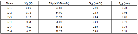
The present work is the study on the performance value of Double Gate (DG) Metal Oxide Semiconductor Field Effect Transistor (MOSFET) with different channel and gate engineering. Six different structures have been proposed and analysed keeping channel length constant. The short channel parameters like sub threshold swing (SS), transconductance (gm), electric field, leakage current (Ioff), electron mobility (µn) and drain induced barrier lowering (DIBL) are analysed and compared between Gate Stack Double Gate (GS-DG), GS-DG-Single Halo (SH), GS-DG-Double Halo (DH), GS-DG Tri-material (TM), GS-DG TM-SH and GS-DG-TM-DH MOSFETs. This work extensively provides the device structures which may be applicable for high speed switching and low power consumption application. In addition, the effects of gate misalignment on source/drain, device characteristics and various short channel parameters have been discussed and analysed. The simulation and parameter extraction have been done by using the commercially available device simulation software ATLASTM.
Keywords: DG-MOSFET, Gate Stack,Single &Double Halo, SS, Short Channel Effects (SCEs), Device Simulator
Cite this paper: K P Pradhan, S K Mohapatra, P K Agarwal, P K Sahu, D K Behera, Jyotismita Mishra, Symmetric DG-MOSFET With Gate and Channel Engineering: A 2-D Simulation Study, Microelectronics and Solid State Electronics, Vol. 2 No. 1, 2013, pp. 1-9. doi: 10.5923/j.msse.20130201.01.
Article Outline
1. Introduction
- Traditional downscaling device technologies have been serving the microelectronic industry over the last three decades. Scaling with new materials & new device structures are now continually improving the performance of device technologies[1-4]. DG-MOSFETs seem to be a very promising candidate owing to its excellent SCEs suppression, higher drive current and transconductance, lower leakage current, better DIBL and better scaling capability compared to the bulk MOSFETs[5-9]. Now efficient Gate Engineering & Channel Engineering for sub-100-nm MOS devices is a major challenge[10].Symmetric dual material & Triple-material gate structures for a DG-MOSFET have better immunity against SCEs[11-15]. In TM-DG MOSFETs, the gate electrode of the device consists of three laterally contacting materials with different work functions. Work function of the material near the source is highest and that near the drain is the lowest for n-channel MOSFETs (the opposite for p-channel). The high work function near the source leads to more rapid acceleration of carriers in the channel and the low work function near the drain leading to reduction in peak electric field at the drain side.However, continual gate oxide scaling requires high k gate dielectric; since the gate oxide leakage increases with reduced physical thickness of gate oxide (SiO2). In order to suppress the gate leakage current with continuous thinning of gate oxide layer, gate oxide stack with high-k materials in the oxide region have been proposed[16]. The high -k gate stack also improve SCEs, DIBL and hot carrier effects, reduced channel length modulation, drain conductance and advance drive current in sub-100 nm regime[17-18].However, for channel lengths below 100 nm, DG MOSFETs still exhibits considerable leakage currents and to overcome this effect, different channel engineering techniques are used. In the past few years, the local high doping concentration in the channel near source/drain junctions have been implemented via lateral channel engineering, e.g. halo or pocket implants. Single halo MOSFET structures have been introduced for bulk as well as for SOI MOSFETs[19-24] to adjust the threshold voltage and to improve the device SCEs.In this paper, GS is considered for all the device structures. GS-DG and GS-DG-TM are compared by taking DH (lateral symmetric channel) & SH (lateral asymmetric channel) techniques. In these structures, the channel is highly doped near the source & drain regions to reduce the width of the depletion region in the vicinity of the junctions. In effect, this reduces sub threshold leakage current and increases output impedance. The gate work-function engineering allows the GS-DG-TM devices to have the same threshold voltage for a reduced doping concentration in the channel region resulting in better immunity to mobility degradation and hence higher transconductance. The characteristics of the GS-DG-TM device are compared with SH & DH doped SOI MOSFETs. This work also highlights one out of the various gate misalignments and its effect on source/drain, device characteristics and various short channel parameters have been discussed and analysed. In this paper, a model for the nanoscale fully depleted symmetrical GS-DG-TM-MOSFET is successfully simulated and studied.
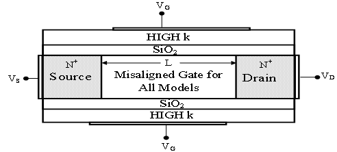
2. Device Structure
- Figure 1.(a)-(f) shows the schematic cross-sectional view of the DG-MOSFETs (n-channel) with different structural models implemented in the 2D device simulator. In the structures, the channel length (L) and Source/Drain length (LS/LD) is kept as 40nm. The silicon thickness (TSi) as 10nm and a uniform density ND as 1020 cm-3 is taken. The channel is doped with impurity concentration of NA=1016 cm-3. In each case the effective oxide thickness is 1.1625nm. The thickness of SiO2 and equivalent HfO2 are 1nm, 0.1625nm respectively. To get equivalent thickness of the high-k as 0.1625nm, the physical thickness is calculated as 1nm according to
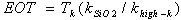 , where Tk is the physical thickness of high-k, k is the permittivity of dielectric material . The work function for the gate electrode is assumed as 4.8ev for single material DG-MOSFETs. The channel engineering SH and DH was implemented in GS-DG models in a ratio of 1:4 and 1:2:1 respectively with NA= 1018 cm-3 as shown in Figure 1(b) &(c). The control gate M1 (toward the source side) and screening gates M2 and M3 (toward the drain side) are the gate electrodes with lengths LM1, LM2 and LM3 (LM1: LM2:LM3 = 1:2:1) and with metal work functions qφM1, qφM2 and qφM3 (4.8ev, 4.6ev &4.4ev).
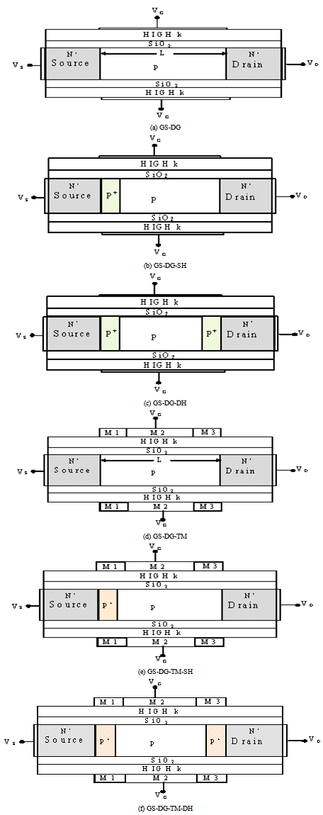 | Figure 1. Schematic structures of DG-MOSFETs with (a) GS-DG (b) GS-DG-SH (c) GS-DG-DH (d) GS-DG-TM (e) GS-DG-TM-SH (f) GS-DG-TM-DH |
3. Simulation
- To obtain accurate results for MOSFET simulation we need to account for the mobility degradation that occurs inside inversion layers. The degradation normally occurs as a result of higher surface scattering near the semiconductor to insulator interface. So, in the simulation, the inversion-layer Lombardi constant voltage and temperature (CVT) mobility model is used, that takes into account the effect of transverse fields along with doping and temperature dependent parameters of the mobility. The Shockley–Read–Hall (SRH) model simulates the leakage currents that exist due to thermal generation. Electrons in thermal equilibrium at given temperature with a semiconductor lattice obey Fermi-Dirac statistics. The use of Boltzmann statistics is normally justified in semiconductor device theory, but Fermi-Dirac statistics are necessary to account for certain properties of very highly doped (degenerate) materials. The model Fermi-Dirac uses a Rational Chebyshev approximation that gives results close to the exact values. The Auger recombination models for minority carrier recombination have been used. Furthermore, we chose Gummel’s method (or the decoupled method) which performs a Gummel iteration for Newton solution[25].
4. Results & Discussion
4.1. Aligned Gate
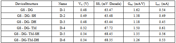
- In Figure 2 (a),(b) IDS-VGS transfer characteristics have been shown on linear scale and log scale for all six different device structures and have been compared for VDS=10 mV and 1.2 V. The GS-DG-TM provides higher drain current in comparison to all other configurations. The halo doping on both, the source and drain end, show a lower drain current because higher doping concentration reduces the surface mobility.
 | Figure 2. Drain Current (ID) in both linear and log scale(inset) as a function of Gate Voltage (VGS) at (a) VDS =0.1V (b) VDS =1.2V for all models |
 | (1) |
 | (2) |
 | (3) |
 | (4) |
 | (5) |
 decreases,
  increases and there is an increase in
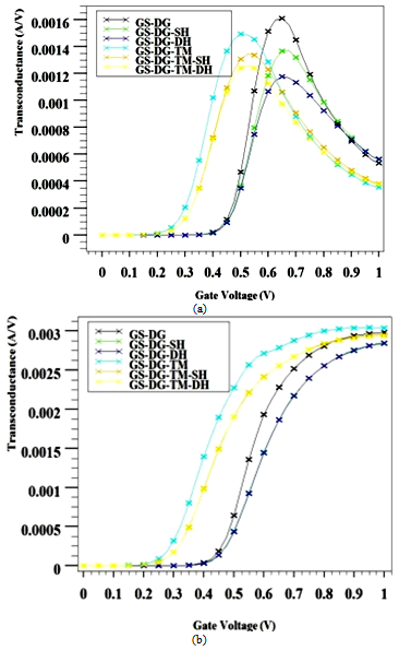
  value which consequently leads to an increase in SS value.The gm versus VGS characteristics have been compared for all six device structures in Figure 3 for VDS=0.1V and 1.2V. As we know:
 | (6) |
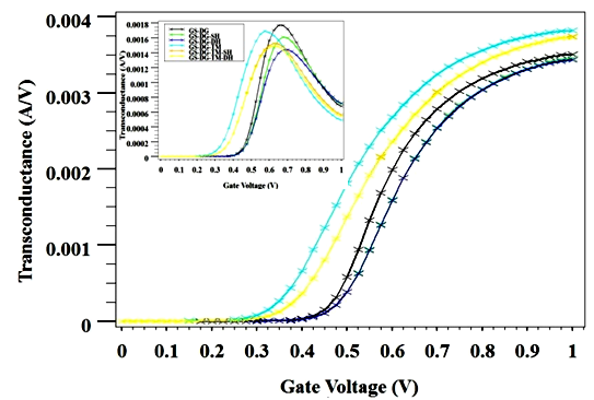 | Figure 3. Variation of gm as a function VGS at VDS =0.1V (inset) and VDS =1.2V for all structures |
|
|
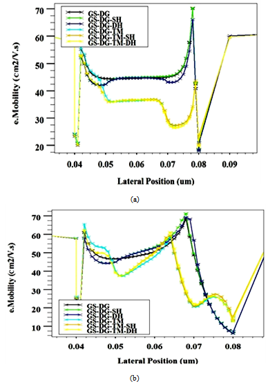 | Figure 4. Electron Mobility along the channel (cutline at Y=4nm) (a) at VDS=0.1V and (b) at VDS=1V for different models |
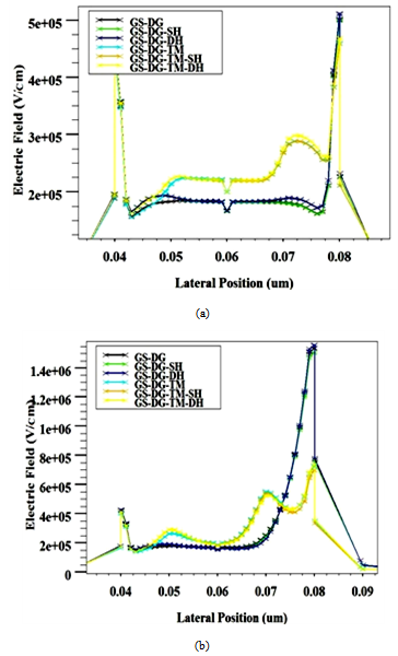 | Figure 5. Electric Field along the channel (cutline at Y=4nm) (a) at VDS=0.1V and (b) at VDS=1V for different models |
|
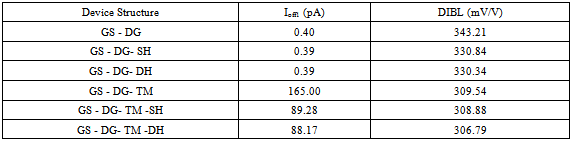
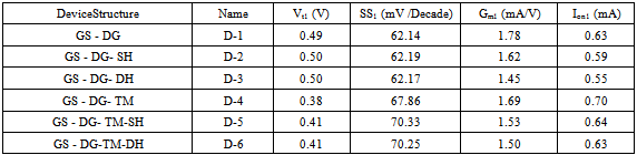
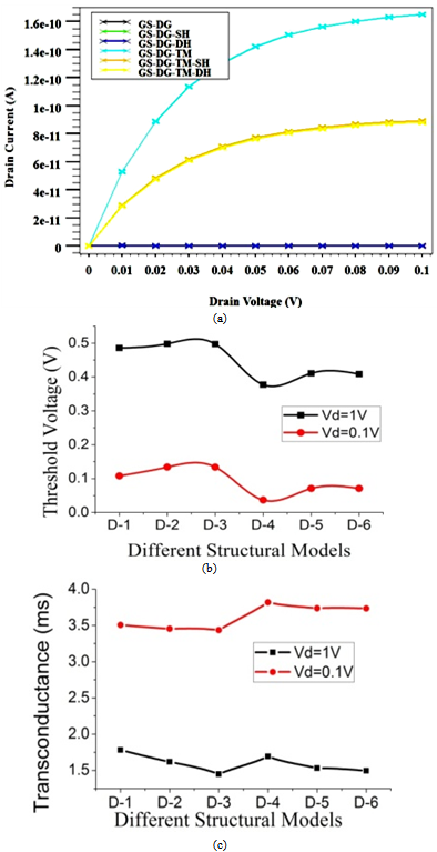 | Figure 6. (a) Curve of Leakage Current (Ioff) as a function of VDS at VGS =0V, (b) & (C) Threshold Voltage (Vt) and Transconductance (Gm) variation of different models |
4.2. Misalignment of Gate
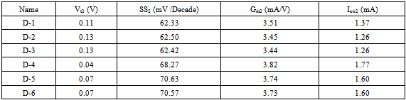
- The fabrication of planer DG-SOI in the sub-100 nm regime with an ideal self-aligned structure is very difficult. The Source/Drain asymmetric effects are produced by the Gate misalignment. Understanding the Source/Drain effects and how to deal with them is very essential. Therefore, in this section, we have analyzed the Source/Drain asymmetry caused by gate non-overlapping. Apart from many possible gate misalignments, here one typical case has been taken into consideration. In this case, it is assumed that the top gate is shifted towards the drain side and bottom gate towards the source side 10nm each.In Fig.7 & 8, the transfer characteristic and transconductance are shown for all the device structures and have been compared for VDS=10 mV and 1.2 V by considering gate misalignment effects. All the possible parameters are extracted from the above figures and a comparison is being made between them as highlighted in Table 4 & 5. By comparing the parameters with the previous parameters that are already discussed in Table 1 & 2 we conclude that there are many effects occurring because of the gate misalignment. The non-ideal effects introduced by gate misalignment can be either from the non-overlapping region or from the overlapping region. In this structure, the non-overlapping region is located towards the drain, so the bottom channel near the drain is weakly controlled by the bottom gate. As a result, the drain potential can easily extends toward the channels through the bottom part of channel region.
 | Figure 7. Misaligned gate for all models |
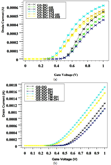 | Figure 8. Drain Current (ID) as a function of Gate Voltage (VGS) at (a) VDS =0.1V (b) VDS =1.2V for all models with one typical misaligned gate |
 | Figure 9. Variation of gm as a function VGS at (a) VDS =0.1V (b) VDS =1.2V for all structures with one typical misaligned gate |
|
|
5. Conclusions
- A close comparison of various design engineering such as the channel and gate engineering on the DG-SOI MOSFETs are studied. The GS engineering along with the halo implantation i.e. GS-DG-SH and GS-DG-DH configurations have demonstrated significant improvements in the device characteristics such as SS value, electron mobility and leakage current. On the other hand by applying gate engineering with halo implantation i.e. GS-DG-TM-SH and GS-DG-TM-DH exhibits a higher value of drain current, the peak transconductance and a lower value of DIBL. In addition, the gate misalignment and its effects on source and drain have also been discussed. The various characteristics and extracted short channel parameters considering gate misalignment have been analysed and a comparison is being shown between them. Therefore, the simulated models in this paper are promising candidates for high speed switching and low power consumption application provided the gate misalignment effects are taken into consideration while fabricating the device.