Sandeep Sharma 1, Rajeevan Chandel 1, Pankaj Kr. Pal 2, Rituraj S. Rathore 3
1E&CE Department, National Institute of Technology-Hamirpur, Hamirpur, 177005, India
2ECE Department, Indian Institute of Technology-Roorkee, Roorkee, 247667, India
3ECE Department, Techno India NJR Institute of Technology, Udaipur, 313001, India
Correspondence to: Sandeep Sharma , E&CE Department, National Institute of Technology-Hamirpur, Hamirpur, 177005, India.
| Email: |  |
Copyright © 2012 Scientific & Academic Publishing. All Rights Reserved.
Abstract
This paper presents performance evaluation of different types of carbon-nanotubes(CNTs) based interconnects viz. Single-walled carbon nanotubes(SWCNT), Bundle SWCNT(B-SWCNT), Multiwalled CNT(M-WCNT) as well as Copper interconnects. The CNT-metal contact resistance has been taken into consideration in the model used in this work. In case of copper interconnects the effect of surface scattering and grain boundary scattering is accounted for. The effect of change in B-SWCNT packaging density on performance of B-SWCNT is analyzed for the first time. A method is proposed to find out the packaging density of a symmetric B-SWCNT structure. SPICE simulations verify the results for 45nm technology node.
Keywords:
Carbon Nanotube, Single Walled Carbon Nanotube, Bundle Single Walled Carbon Nanotube, Multiwalled Carbon Nanotube, Mcnt
1. Introduction
According to the ITRS[1] the interconnect dimensions will become smaller and smaller down to nanometric regime in the near future. As the interconnect size is scaled down, the resistivity of the copper increases mainly due to grain and surface scattering effects. This effect along with the higher current densities requirement that must be carried by the future interconnects makes the copper interconnects more and more vulnerable to electro migration failure in the near future. In addition it is also observed that at 130 nm technology node approximately 51% of microprocessor power was consumed by interconnect. It is also projected that without changes in design philosophies, in the next five years up to 80% of microprocessor power will be consumed by interconnect[2].The CNTs have the potential to provide solution for the resistivity and electro migration problems faced by the copper interconnects in deep submicron technology. The high current densities, increased reliability, promising electrical, thermal and mechanical properties of the CNTs make them the attractive candidate for next generation integrated circuit(IC) applications[3].This paper is based on the authors work in[4] where electrical modelling(R, L, C) of various types of CNT basedinterconnects like Single Walled CNT(SWCNT), Bundle Single Walled CNTs(B-SWCNT) both for perfectly metallic and the most naturally occurring case(one- third metallic) and Multiwalled CNTs(MWCNTs) is done at 45 nm technology node. The paper presents the results of the authors work in[4].It is shown that under the most practical conditions(actual interconnect dimensions as per ITRS) only the MWCNTs can give better performance in terms of delay than Copper and all other types of CNT based interconnects at local, intermediate and global interconnect levels. The MWCNTs are easier to fabricate with less concern about chirality and density control can thus act as an replacement for traditional Copper interconnects at local, intermediate and global interconnect levels.It is also found that under the most practical conditions (actual interconnect dimensions as per ITRS) the SWCNTs can give the best performance in terms of power. Both the SWCNT and MWCNT outperforms the copper interconnects in terms of average power dissipation at local, intermediate and global interconnect levels. While it is found that the B-SWCNTs are not able to outperform copper interconnects presently in terms of both speed and power.
2. Previous Work
Several studies have been carried out to investigate the performance of CNT based interconnects. The work in[5] shows that the densely packed CNT bundle can provide an improvement in the interconnect speed. However the work in[5] assumes the inter-tube spacing in SWCNT to be 0. The work in[4] takes into account the minimum inter-tube spacing observed in SWCNT bundles which is 0.32 nanometer(characteristic of Van der Waal intertube binding) to arrive at more accurate results for CNT based interconnect parasitic. The work in[6] proposed a compact RLC model and made a comparison with copper interconnect. However, in these studies, it was assumed that the contact between metal and nanotube is perfect and all CNT bundles are completely densely packed. In fact it cannot be realized by present technologies. The treatment of the critical issue of CNT interconnect capacitance in[7] also raises concern. While carrying out comparison of CNT interconnect performance with copper interconnect the copper interconnect was modelled as coaxial cable[3]. However, in the authors work in[4] copper interconnect is modelled as a microstrip line[8] which is supposed to be the most widely used model for copper interconnect modeling. Moreover the work in[3] doesn’t take into account the effect of grain and surface scattering on copper interconnect resistivity. The work in[4] take into account the effect of metal-nanotube interconnect contact resistance as well as grain and surface scattering on copper interconnect resistivity to arrive at the best possible results.For taking into account the effect of change in packaging density of B-SWCNT on its performance a simple method to find the packaging density of a symmetric B-SWCNT structure and kinetic inductance has been proposed in[4]. This work also takes into account the minimum inter-tube spacing observed in SWCNT bundles which is 0.32nm(characteristic of Van der Waal intertube binding). In the previous modelling efforts in the literature the intertube spacing was not taken into account. In a Bundle-SWCNT all the SWCNTs are not conducting(metallic). Also the fabrication techniques not always result in such a dense bundle of SWCNTs. In[4] the sparsely populated bundles and the presence of non-metallic CNTs(which do not contribute to current conduction) are accounted for by taking a larger center-to-center distance between adjacent conducting mCNTs.Fig. 1 and Fig. 2 show the electrical model for SWCNT and MWCNT interconnect[4].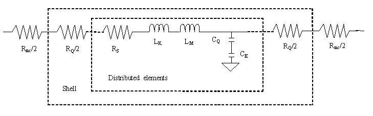 | Figure 1. Model of a SWCNT interconnect |
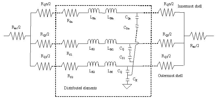 | Figure 2. An MWCNT interconnect model with n number of shells |
3. Results & Discussions
3.1. Simulation Methodology
The circuits in Fig. 1 and Fig. 2 are simulated in SPICE. The simulated and analytical results for 45nm technology nodes for delay and power for SWCNT, B-SWCNT(Fm=1), B-SWCNT(Fm=1/3) and copper interconnect are shown in following figures. However for MWCNT only the simulated results have been tabulated.
3.2. Delay Analysis of Interconnects
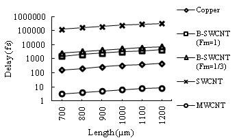
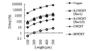
The delay variation with interconnect length for different types of interconnects at local, intermediate and global interconnect level are presented in Figs. 3 to 5.It can be seen from Fig. 3 to Fig. 5 that the delay for all interconnect levels i.e. local, intermediate and global(for 45 nm technology node) follows the trend “Delay MWCNT”< “Delay Cu”< “Delay B-SWCNT(Fm=1)”< “Delay B-SWCNT(Fm=1/3)”< “Delay SWCNT”.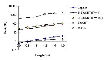 | Figure 3. Delay comparison for Local interconnects |
 | Figure 4. Delay comparison for Intermediate interconnect |
 | Figure 5. Delay comparison for Global interconnect |
The conductance of the MWCNT is obtained by the summation of conductance of all its shells in other words the resistance of the MWCNT is very small because the shells appears to be in parallel and also the CNT-metal contact resistance for MWCNT is 0. The capacitance of MWCNT is also therefore very low hence the net RC product is very small for MWCNT and hence its delay. In case of B-SWCNT there capacitance is much higher than that of copper interconnect despite having low resistance value. While in case of SWCNT there capacitance is lower than the capacitance of copper interconnect but there resistance is very high in comparison to the resistance of copper or even B-SWCNTs.These results obtained from SPICE simulations are verified by analytical modeling for all the types of interconnects.From Fig. 3 to Fig. 5 it can also be concluded that as the number of CNTs in a B-SWCNT is reduced than the CNT interconnect delay increases. However, it is also observed that the effect of decrease in the number of CNTs in a B-SWCNT on delay is reduced as the length of the interconnect increases. That is to say that the difference between the delay of B-SWCNT(Fm=1) and B-SWCNT(Fm=1/3) is very small at global interconnect level compared to their difference in delay at local and intermediate interconnect level.As far as performance in terms of delay is concerned the isolated SWCNTs give the poorest performance and MWCNTs gives the best performance and can be considered as a replacement for copper interconnects if speed is the design criteria. At present the B-SWCNT doesn’t seem to be outperforming copper interconnect technology in terms of speed. However if the fabrication techniques of B-SWCNTs is improved so that there capacitance can be reduced then these can prove to be a competitive candidate along with MWCNT for replacement of traditional copper interconnect technology in the near future.
3.3. Average Power Dissipation in Interconnects
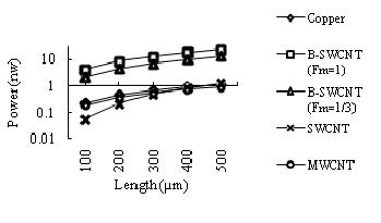
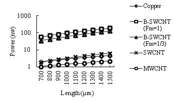
The average power dissipation by different types of interconnects at local, intermediate and global interconnect level are plotted in Fig. 6 to Fig. 8.It can be seen from Fig. 6 to Fig. 8 that the the average power dissipation for local and intermediate interconnect level(for 45 nm technology node) follows the trend “Avg Power SWCNT”< “Avg Power MWCNT”< “Avg Power Cu”< “Avg Power B-SWCNT(Fm=1/3)”< “Avg Power B-SWCNT(Fm=1)”.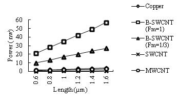 | Figure 6. Average power dissipation for Local interconnects |
 | Figure 7. Average power dissipation for Intermediate interconnects |
 | Figure 8. Average power dissipation for Global interconnects |
However the average power dissipation for global interconnects is observed to follow the trend as “Avg Power MWCNT< “Avg Power Cu”< Avg Power SWCNT”< “Avg Power B-SWCNT(Fm=1/3)”< “Avg Power B-SWCNT (Fm=1)”The capacitance of SWCNT plays an important role in determining its average power dissipation. Since the SWCNT capacitance is least among all the different kinds of CNT based interconnect and even less than that of copper therefore SWCNT average power dissipation is least for local and intermediate interconnects. However at global interconnect level MWCNT interconnect outperforms SWCNT interconnect. The reason for the low power dissipation for MWCNT interconnect can be given to the low value of resistance and inductance of MWCNT compared to that of B-SWCNT and Copper interconnect which is due to the fact that the shells of the MWCNT appears in parallel which drastically reduce the MWCNT interconnect resistance and inductance.The above trends are general trend however they have some exceptions like at global interconnect level at 45 nm technology node the average power dissipation by copper and SWCNT interconnects are almost comparable and on further scaling of global interconnects the copper interconnect may almost outperforms SWCNT in terms of power dissipation.Thus we can conclude that the MWCNTs are an ideal replacement option for copper interconnects in terms of power dissipation as they dissipate the least average power among all the types of CNTs and copper interconnect. Thus we can conclude that SWCNT is a better option than copper or B-SWCNT(Fm=1) and B-SWCNT(Fm=1/3) for local and intermediate interconnect level in terms of average power dissipation. At global interconnect level the SWCNT is not a better option than copper interconnect in terms of average power dissipation.These trends obtained from simulation are verified by analytical modeling. However the difference in analytical and simulation results for average power dissipation is much less for global interconnects as compared to local and intermediate interconnect.It is also observed that as the number of CNTs in a B-SWCNT is reduced than the CNT interconnect power dissipation decreases. However, it is also observed that the effect of decrease in the number of CNTs in a B-SWCNT on power dissipation is reduced for global interconnect level.
3.4. Power-Delay-Product Interconnect Performance
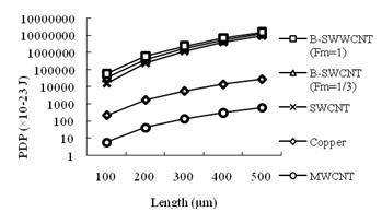
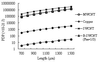
Power-Delay-Product(PDP) is an important metric for design of all electronic circuits. PDP is the measure of energy dissipation in a system. Therefore PDP should be least for the best circuit. Fig. 9, Fig. 10 and Fig. 11 show the PDP results for local, intermediate and global interconnects for 45nm technology node.It can be seen from Fig. 9 and Fig. 11 that for local and intermediate level the PDP follows the trend as “PDP MWCNT< PDP Copper< PDP SWCNT< PDP B-SWCNT(Fm=1/3)< PDP B-SWCNT(Fm=1)”. From Fig. 11 the PDP trend for global interconnect level is “PDP MWCNT< PDP Copper< PDP B-SWCNT(Fm=1) ≈ PDP B-SWCNT(Fm=1/3)< PDP SWCNT.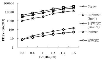 | Figure 9. Power-Delay-Product(PDP) for local interconnect |
 | Figure 10. Power-Delay-Product(PDP) for intermediate interconnect |
 | Figure 11. Power-Delay-Product(PDP) for global interconnect |
It is concluded that MWCNT has the minimum Power-Delay-Product among all the different types of VLSI interconnects. Therefore MWCNT interconnect is the best among different interconnects used for electronic circuits. MWCNT interconnects can thus replace traditional copper based interconnect technology for VLSI circuits. At the local and intermediate interconnect levels the perfectly metallic bundle SWCNT(Fm=1) has the highest PDP while at global interconnect level SWCNT has the highest PDP. The high value of PDP of B-SWCNTs and SWCNT compared to PDP of copper interconnect restricts their use as VLSI interconnects at local, intermediate and global interconnect levels.
4. Conclusions
In this work different types of CNTs viz. SWCNT, B-SWCNT(Fm=1), B-SWCNT(Fm=1/3) and MWCNT along with copper interconnect are modeled for their application as VLSI interconnect. The data provided by ITRS for local, intermediate and global interconnects for 45nm technology node is used. After modeling the parasitic of different CNTs and copper interconnect their performance parameters viz. delay and power are analyzed. A method to find the number of conducting CNTs in a Bundle-SWCNT interconnects is proposed. The simulated values are verified analytically and match well. It has been found that the MWCNT interconnects outperforms the traditional copper interconnects in terms of performance parameters viz. delay and power. Hence MWCNT based interconnect technology is suggested as a replacement for the traditional copper interconnect technology.From this modelling work it can also be concluded that under the most practical conditions of interconnect dimensions(dimensions supplied by ITRS for interconnects for 45nm technology node) the SWCNT, B-SWCNT both perfectly metallic(Fm=1) and the most natural case(Fm=1/3) of bundle SWCNT fail to give better performance than copper interconnects in terms of delay(speed).However, in terms of average power dissipation the SWCNT gives the best performance among all the different types of CNTs at local and intermediate interconnect level and even outperforms the copper interconnects. Thus if the design criteria is only power saving than SWCNT can be looked upon as a good option for local and intermediate interconnects. However there large delay limits their application as interconnects. As far as performance of B-SWCNT interconnect is concerned we find that at present they don’t offer any advantage over copper interconnect technology. However at global interconnect level the difference in the delay between B-SWCNT interconnect and copper interconnect is much lesser compared to their delay difference at local and intermediate interconnect level. It has also been found that reducing the number of conducting CNTs in Bundle SWCNT degrades the performance of Bundle SWCNT in terms of delay but significantly improves the performance of Bundle-SWCNT in terms of power dissipation.It has also been found that MWCNT has the minimum Power-Delay-Product among all the different types of VLSI interconnects. Therefore MWCNT interconnect is the best among different interconnects used for electronic circuits. MWCNT interconnects can thus replace traditional copper based interconnect technology for VLSI circuits. At the local and intermediate interconnect levels the perfectly metallic bundle SWCNT(Fm=1) has the highest PDP while at global interconnect level SWCNT has the highest PDP. The high value of PDP of B-SWCNTs and SWCNT compared to PDP of copper interconnect restricts their use as VLSI interconnects at local, intermediate and global interconnect levels.
References
| [1] | International Technology Roadmap for Semiconductors, 2003: http://public.itrs.net/. |
| [2] | N. Magen, A. Kolodnv, N. Shamir, “Interconnect power dissipation in a microprocessor,” ACM system – level interconnect prediction workshop, Feb 2004. |
| [3] | N. Srivastava and K. Banerjee, “Performance analysis of carbon nanotube interconnects for VLSI applications, “IEEE/ACM Intl. Conf. on ICCAD, 2005, pp. 383-390. |
| [4] | S. Sharma, R. Chandel, “Modeling and Performance Analysis of Different Types of Interconnects of CNT and Copper Interconnects,” Thesis, 2010. |
| [5] | N. Srivastava, H. Li, K. Banerjee and F. Kreupal, “On the applicability of SWCNTs as VLSI interconnects,” IEEE transactions on nanotechnology, vol. 8, no. 4, pp. 542-559, July 2009. |
| [6] | A. Naeemi, R. Sarvari, and J. D. Meindl, “Performance comparison between carbon nanotube and copper interconnects for gigascale integration(GSI),” IEEE Electron Device Letters, vol. 26, no. 2, pp. 84-86, 2005. |
| [7] | A. Raychowdhury and K. Roy, “Modeling of metallic carbon-nanotube interconnects for circuit simulations and comparison with Cu interconnects for scaled technologies, ”IEEE Trans. Computer-Aided Design of Integrated Circuits and Systems, vol. 25, no. 1, pp. 58-65, 2006. |
| [8] | N. Srivastava, H. Li, K. Banerjee and F. Kreupal, “circuit modeling and performance analysis of MWCNT interconnects,” IEEE transactions on electron devices, vol. 55, no. 6, pp. 1328-1337, June 2008. |
 Abstract
 Reference
 Full-Text PDF
 Full-Text HTML