Keng-Ming Liu , Yung-Yu Hsieh
Department of Electrical Engineering, National Dong Hwa University, Hualien, 974-01, Taiwan
Correspondence to: Keng-Ming Liu , Department of Electrical Engineering, National Dong Hwa University, Hualien, 974-01, Taiwan.
| Email: |  |
Copyright © 2012 Scientific & Academic Publishing. All Rights Reserved.
Abstract
In this paper we use the commercial semiconductor device simulator, Sentaurus, to simulate the electrical characteristics of sub-30nm multiple-gate (MG) silicon-on-insulator (SOI) MOSFETs. The gate configurations of the simulated MG SOI MOSFETs include: single-gate (SG), two kinds of double-gate (DG), triple-gate (TG), and gate-all-around (GAA). We examine the effects of the dimensions of the gate length, fin height, fin width, and the transport models for each gate configuration. The simulation results can serve as the guidelines of device design and they indicate that as the gate length scales down to 15 nm below, only GAA, TG, and DG configurations with specific fin cross-section dimensions can meet the device requirements.
Keywords:
Device Simulation, Multiple-Gate, MOSFET, TCAD, SOI, Dimension
1. Introduction
As the channel length of MOSFETs keep scaling down within nanometer scale, the short channel effects (SCEs) become so detrimental that the conventional planar bulk MOSFET structure shows poor device performance. To improve the gate control over the channel region, the multiple-gate (MG) MOSFET structure has been proposed and studied by both fabrication[1-6] and simulation[7-13]. It is believed that there is a great possibility for the MG MOSFET structure to be used in the 22-nm VLSI technology node and the following nodes. Furthermore, silicon-on- insulator (SOI) MG MOSFET structure has been considered as the ultimate device structure in the future. In this paper, we use the mainstream technology CAD (TCAD) tools in industry, Sentaurus (which is the product of Synopsys Inc.), to simulate various gate configurations and dimensions for the SOI MG MOSFET structure. Most of the previous simulation studies on SOI MG MOSFETs focused on the specific gate configurations[8-11]. In this paper, we simulate all the possible gate configurations for the SOI MG MOSFETs: single-gate (SG), double-gate (DG), triple-gate (TG), and gate-all-around (GAA) configurations. The similar simulation study has been made before[7], however, the gate lengths of the simulated devices are above 30 nm therein. In this work, we investigate the device characteristics of the SOI MG MOSFETs with the gate length less than 30 nm by 3D TCAD simulation and also examine theeffects of the transport models on the device simulation results.
2. Device Structure and Simulation Approach
Figure 1 shows the simulated gate configurations for the SOI MG MOSFET structure. The gate configurations include: SG, DG, TG, and GAA configurations. Note that the DG configuration has two types: (1) the two gates are in parallel (DG-1) and (2) the two gates are connected (DG-2). All gate configurations have 10Å gate oxide (SiO2) and 20 nm source and drain regions. For simplicity, we assume that the junctions are abrupt and there is no overlap or underlap between the gate and the source/drain. The doping concentration in the source and drain regions is n-type 1020 cm-3 and that in the channel region is p-type 51018 cm-3. The work-function difference is adjusted to make each simulated device has a threshold voltage of 0.3 V. Simply using the n+ polysilicon gate without adjusting the work-function difference will result in a negative threshold voltage for the SOI MG MOSFETs presented here. The supply voltage, VDD, is set to be 1 V. The values of the gate oxide thickness, channel doping, threshold voltage, and supply voltage are chosen according to the 2009 International Technology Roadmap for Semiconductors (ITRS). The gate length, fin height, and fin width are varied from 15 to 30 nm, 10 to 20 nm, and 10 to 20 nm, respectively. In this work, we focus on examining the effects of the dimensions of the gate length, fin height, and fin width of the SOI MG MOSFETs.Device simulation was performed by Sentaurus. Figure 2 shows the simulation flow. First, we use the Sentaurus Structure Editor (SSE) to define the desired device structures and the associated parameters. Then we put the outcome of SSE into the Sentaurus Device (SDevice) to simulate the device characteristics. There are at least two transport models which are available in SDevice: drift-diffusion (DD) model and hydrodynamic (HD) model. The simulation results of these two models will be shown in the following. The HD model includes the carrier temperature effect and the energy current in addition to the electron and hole currents which are considered by the DD model. Therefore, we expect the simulation results from the HD model should be more accurate. Besides the DD and HD models, we also examine the effects of quantum confinement by including the density gradient (DG) model into the SDevice simulation. To include quantization effects, SDevice uses a potential quantity Λn in the classical electron density formula [14]: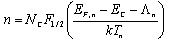 | (1) |
where NC is the effective density of states in the conduction band and F1/2( • ) is the Fermi-Dirac integral. Similarly, there is a Λp for holes. For density gradient model, Λn is given by [14]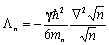 | (2) |
where γ is a fit factor. Since n is Λn-dependent, (2) needs to be solved numerically.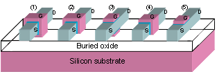 | Figure 1. Different gate configurations for the SOI MG MOSFETs. The gate configurations include: (1) GAA, (2) TG, (3) DG-1, (4) DG-2 and (5) SG configurations |
 | Figure 2. Simulation flow of Sentaurus TCAD tools [14] |
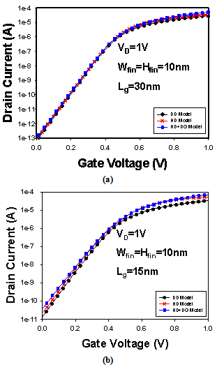 | Figure 3. The ID-VG curves of the GAA MOSFETs with (a) 30-nm or (b) 15-nm gate length and 1010 nm2 fin cross section under different transport models (DD, HD, and HD+DG) |
| Table 1. The Electrical Characteristics of the GAA MOSFETs with 15-nm Gate Length and 1010 nm2 Fin Cross Section under Different Transport Models (DD, HD, and HD+DG) |
| | Model Characteristics | DD | HD | HD+DG | | SS (mV/dec) | 79.7 | 80.9 | 86.6 | | DIBL (mV) | 84 | 99 | 107 | | Ion (A) | 4.0×10⁻⁵ | 5.54×10⁻⁵ | 7.16×10⁻⁵ | | Ioff (A) | 1.44×10⁻¹¹ | 2.22×10⁻¹¹ | 4.22×10⁻¹¹ | | Ion/Ioff | 2.36×10⁶ | 2.39×10⁶ | 1.7×10⁶ |
|
|
Figure 3 shows the ID-VG curves of the GAA MOSFETs with 30-nm or 15-nm gate length and 1010 nm2 fin cross section under different transport models (DD, HD, and HD+DG). For the 30-nm gate length, the simulation results of different transport models are very close. However, as the gate length reduces to 15 nm, the difference caused by using different transport model is obvious. Table 1 shows the electrical characteristics of the 15-nm GAA MOSFET under different transport models which are derived from Figure 3. For 15-nm gate length, using either DD or HD model only may overestimate the subthreshold swing (SS) and adopting DD model only may underestimate the current drive. The degradation of SS caused by including the DG model is due to the increase of the effective oxide thickness (EOT) as quantum confinement is considered. We believe that using HD model combined with DG model should be more realistic for the nanoscale devices. Therefore, all the following simulation results are based on HD model combined with DG model.
3. Simulation Results and Discussion
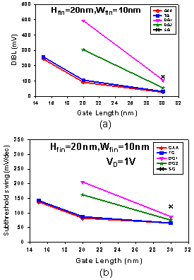
There are actually four fin cross sections for the simulated SOI MG MOSFETs as shown in Figure 4: (1) 2020 nm2, (2) 2010 nm2 (fin height fin width), (3) 1020 nm2, and (4) 1010 nm2. Figures 5, 6, 7, and 8 show the drain-induced barrier lowering (DIBL) and the subthreshold swing (SS) of the SOI MG MOSFETs with these four cross sections (Figure 4) as the gate length decreases from 30 nm to 15 nm under different gate configurations. The DIBL is defined as the difference in threshold voltage when the drain voltage is increased from 0.05 V to 1 V. As shown in Figure 5, there is no gate configuration can have a DIBL value below 600 mV or a SS value below 300 mV/dec for the 15-nm gate-length SOI MG MOSFETs with the 2020 nm2 fin cross section. The smaller fin cross section shows the better DIBL and SS as shown in Figure 8. The GAA configuration has the best DIBL and SS for any fin cross section. However, for the 2010 nm2 and 1020 nm2 fin cross sections, the device characteristics of the TG and DG-1 configurations, respectively, are comparable to those of the GAA configuration as shown in Figures 6 and 7. The DG-1 configuration has better performance than the DG-2 configuration except for the 2010 nm2 fin cross section since the gate width of the DG-1 configuration is small (10 nm per gate) in this case. In general, more gate coverage results in better immunity against SCEs. Table 2 is the summary for the device characteristics of the 15-nm gate-length GAA MOSFETs under different fin cross sections. The device with the 1010 nm2 fin cross section has the best device performance and the SS and on-off current ratio are 86.6 mV/dec and 1.7×10⁶, respectively.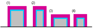 | Figure 4. Four fin cross sections for the simulated SOI MG MOSFETs: (1) 2020 nm2, (2) 2010 nm2 (fin height fin width), (3) 1020 nm2, and (4) 1010 nm2. Here the TG configuration is used as an illustration. |
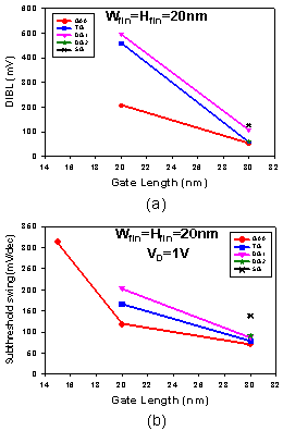 | Figure 5. (a) DIBL and (b) SS of the SOI MG MOSFETs with the fin cross section 2020 nm2 as the gate length decreases from 30 nm to 15 nm under different gate configurations. |
 | Figure 6. (a) DIBL and (b) SS of the SOI MG MOSFETs with the fin cross section 2010 nm2 (fin height fin width) as the gate length decreases from 30 nm to 15 nm under different gate configurations. |
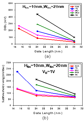 | Figure 7. (a) DIBL and (b) SS of the SOI MG MOSFETs with the fin cross section 1020 nm2 (fin height fin width) as the gate length decreases from 30 nm to 15 nm under different gate configurations. |
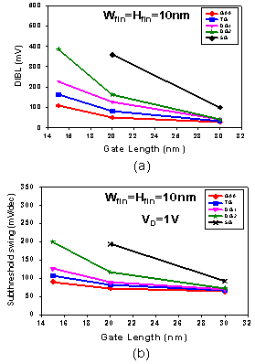 | Figure 8. (a) DIBL and (b) SS of the SOI MG MOSFETs with the fin cross section 1010 nm2 as the gate length decreases from 30 nm to 15 nm under different gate configurations. |
| Table 2. Summary for the Device Characteristics of the 15-nm Gate-Length GAA MOSFETs under Different Fin Cross Sections (Fin Height Fin Width) |
| | CharacteristicsHeight× Width | SS(mV/ dec) | DIBL(mV) | Ion (A) | Ioff (A) | Ion/ Ioff | | 20 × 20 nm2 | 314.2 | NA | 1.86×10⁻⁴ | 4.84×10⁻⁷ | 3.83×10² | | 20 × 10 nm2 | 137.7 | 243 | 1.2×10⁻⁴ | 2.41×10⁻⁹ | 4.97×10⁴ | | 10 × 20 nm2 | 133.7 | 230 | 1.31×10⁻⁴ | 3.81×10⁻⁹ | 3.44×10⁴ | | 10 × 10 nm2 | 86.6 | 107 | 7.16×10⁻⁵ | 4.22×10⁻¹¹ | 1.7×10⁶ |
|
|
4. Conclusions
In this work, we have investigated the effects of various fin dimensions on the device characteristics of the SOI MG MOSFETs with the SG, DG-1, DG-2, TG, and GAA configurations. The simulation results indicate that the smaller fin cross section and higher gate-coverage ratio will result in the better SCE immunity. The GAA configuration has the best device performance for any fin cross section. For some rectangular fin cross sections, the device characteristics of the TG and DG-1 configurations are comparable to those of the GAA configuration. For the 15 nm gate length, only GAA, TG, and DG-1 configurations with particular fin cross-section dimensions can fulfill the device requirements.
ACKNOWLEDGEMENTS
This work is supported by Taiwan National Science Council (NSC) under Contract NSC-100-2221-E-259-003. We are also grateful to the Taiwan National Center for High-performance Computing for computing facilities.
References
| [1] | F. L. Yang et al., “5nm-gate nanowire FinFET,” in Proc. VLSI Symp. Tech. Dig., 2004, pp. 196-197. |
| [2] | S. D. Suk et al., “High-performance twin silicon nanowire MOSFET(TSNWFET) on bulk Si wafer,” IEEE Transactions on Nanotechnology, vol. 7, no. 2, pp. 181-184, 2008. |
| [3] | D. Hisamoto et al., ”FinFET-A self-aligned double-gate MOSFET scalable to 20 nm,” IEEE Transactions on Electron Devices, vol. 47, no. 12, pp. 2320-2325, 2000. |
| [4] | B. Yu et al., “FinFET scaling to 10 nm gate length," in Tech. Digest, IEDM, 2002, pp. 251 - 254. |
| [5] | C. Y. Chang et al., ”A 25-nm gate-length FinFET transistor module for 32nm node,” in Tech. Digest, IEDM, 2009, pp. 293 - 296. |
| [6] | X. Huang et al., ”Sub-50nm p-channel FinFET,” IEEE Transactions on Electron Devices, vol. 48, no. 5, pp. 880-886, 2001. |
| [7] | J. T. Park and J. P. Colinge, ”Multiple-gate SOI MOSFETs: device design guidelines,” IEEE Transactions on Electron Devices, vol. 49, no. 12, pp. 2222-2229, 2002. |
| [8] | J. Y. Song, W. Y. Choi, J. H. Park, J. D. Lee, and B. G. Park, “Design optimization of gate-all-around(GAA) MOSFETs,” IEEE Transactions on Nanotechnology, vol. 5, no. 3, pp. 186-191, 2006. |
| [9] | Y. Song, Q. Xu, H. Zhou, and X. Cai, “Design and optimization considerations for bulk gate-all-around nanowire MOSFETs,” Semiconductor Science and Technology, vol. 24, no. 10, 105006, 2009. |
| [10] | J. W. Yang, P. M. Zeitzoff, H. H. Tseng, “Highly manufacturable double-gate FinFET with gate-source/drain underlap,” IEEE Transactions on Electron Devices, vol. 54, no. 6, pp. 1464-1470, 2007. |
| [11] | G. Pei, J. Kedzierski, P. Oldiges, M. Ieong, C. C. Kan, ”FinFET design considerations based on 3-D simulation and analytical modeling,” IEEE Transactions on Electron Devices, vol. 49, no. 8, pp. 1411-1419, 2002. |
| [12] | J. P. Colinge, “Multiple-gate SOI MOSFETs,” Solid-State Electronics, vol. 48, no. 6, pp. 897-905, 2004. |
| [13] | M. Bescond, K. Nehari, J. L. Autran, N. Cavassilas, D. Munteanu, M. Lannoo, “3D quantum modeling and simulation of multiple-gate nanowire MOSFETs,” in Tech. Digest. IEDM, 2004, pp. 617-620. |
| [14] | Sentaurus Device User Guide, Version C-2009.06, Synopsys. |
 Abstract
 Reference
 Full-Text PDF
 Full-Text HTML