-
Paper Information
- Next Paper
- Previous Paper
- Paper Submission
-
Journal Information
- About This Journal
- Editorial Board
- Current Issue
- Archive
- Author Guidelines
- Contact Us
Microelectronics and Solid State Electronics
2012; 1(3): 60-63
doi: 10.5923/j.msse.20120204.02
Radiation Effect on Optical and Electrical Properties of CdSe(In)/P-Si Heterojunction Photovoltaic Solar Cells
 Abstract
 Reference
 Full-Text PDF
 Full-Text HTML
M. Ashry , S. Fares
National Center for Radiation Research and Technology (NCRRT), AEA,P.O. 29 Nasr City Egypt
Correspondence to: S. Fares , National Center for Radiation Research and Technology (NCRRT), AEA,P.O. 29 Nasr City Egypt.
| Email: |  |
Copyright © 2012 Scientific & Academic Publishing. All Rights Reserved.
The efficiency and radiation resistance of solar cells are graded up. They are, then, fabricated in the form n-CdeSe (In)/P-Si Heterojunction cells by electron beam evaporation of a stoichiomteric mixture of CdSe and In to make a thin film on a P-Si single crystal wafers with thickness 100 µm and resistivity ~ 1.5 Ω.cm at a temperature 473 ok . The short-circuit current density (jsc), open-circuit voltage (Voc), fill factor (ff) and conversion efficiency (η) under Am1 are 20 mA/cm2 , 0.49 V, 0.71 and 6% respectively . The cells were exposed to different electron doses (electron beam accelerator of energy 1.5 MeV, and beam intensity 25 mA). The cells performance parameters are measured and discussed before and after irradiation.
Keywords: N-Cdse(In)/P-Si Solar Cells Performance, Electron Beam , Radiation Effects
Article Outline
1. Introduction
- The output power for space solar cells can be increased by improving in the efficiency (η) and the radiation resistance. In such case radiation resistance is an important factor, since the continuous impact of high energy particles damages the semiconductor lattice, degrading the cell performance and, hence limiting their lifetime[1,2].The development of a new generation of highly efficient photovoltaic cells GaAs, AlGaAs/GaAs, InP, CdSe/ Ge, Si and others[3-6] is of real interest for future space power applications. Solar cells employing new material are to be more resistant to radiation effect than Si – cells[3] Heterojunction cells n-CdSe/p-Si using silicon as an absorber show different advantages including its easier fabrication as compared wit conventional Si-hemojuncation cells[7-13]. CdSe is an important group II-VI direct band gap (visible) semiconductor material with attractive electronic, spintronics and optoelectronic properties. It has shown great potential in the applications, such as biosensing/bioimaging, light emitting diode, and photodetectors The CdSe (In) films have high conductivity due to the add indium (In) and therefore, they are very suitable as a window layer for solar cells. In these cells, most carriers are generated in the base (Si), so that the control of the thickness and doping of the window layer (CdSe) is lea critical. In addition, n-CdSe/p-Si structure can be prepared by low temperature processes (evaporationsputtering or chemical spray), thereby avoiding lifetime degradation[14-16], which is suitable for low cost space solar cells.Furthermore, this structure has no energy spikes[7] and the surface recombination velocity seen in hemojuncation can be neglected .Low resistivity CdSe films are needed in heterojunction solar cells to lower the cell series resistance, to confine the band bending to the narrow band gap material and to minimize the conduction band-Fermi level energy gap[17].The cells were fabricated at different compositions of CdSe (In: CdSe weight ratio) and thicknesses. In this work, the n-CdSe/p-Si solar cell was fabricated by electron beam evaporator of a stoic ion mixture of CdSe and In forming a film on a p-Si instead of individual evaporation for CdSe as has been presented in pervious works[7,14-16]. The effect of fabrication condition and irradiation with gamma radiation and electron beam on optical and electrical properties of heterojunction solar cells were investigated.
2. Cell Fabrication
- In this method, the composition (namely 4:1000 and 6:1000 weight) for the Indium (In) to CdSe is chosen for n-CdSe (In)/p-Si structure. Each composition in a well cleaned sealed silica tube under a vacuum of 3x10⁻⁵ Torr. Then the temperature of the mixture was increased gradually, with 278°k/min in microprocessor coprolite furnace up to temperature for 1223°k and kept at this temperature for about 5 hours. As a result, we got a stoichiomteric mixture of CdSe and In after cooling it gradually to the room temperature. On the other hand, the p- Si(111) – of 1.5 Ω.cm resistivity was cleaned first in a bath of antigrease Acetone and then was etched for 3 min. in a CP4 solution (15 cm3 HF, 25 cm3 Acetate acid) to remove any oxides.Secondly, it was rinsed for 3 min. in deionized water and finally was dried carefully in a furnace at a temperature of 423ok. After cleaning, the unpolished surface of the silicon wafer was coated with Indium (In) by thermal evaporation in vacuum of 2x10⁻⁵ Torr for back contact formation. After that, the Heterojunction n-CdSe(In)/p-Si structure was fabricated by a vacuum evaporation of CdSe(In) mixture, witch was put in a single boot, to be deposited on a single crystal p-Si substrate at temperature 473 ok with evaporation rat of 5 oA /sec . The upper Al-grid contact coating followed the junction formation by using a suitable mask. At the end the cells were annealed at 523 ok for 2 hour, to activate the junction formation. As a result, a Heterojunction photovoltaic solar cells of area of 2 cm2 with different composition and CdSe layer thicknesses were fabricated as presented in table.(1) Also, the layer thicknesses were deposited at the same time and same previous condition on a glass substrate (12 samples) for measuring its optical transmission. The samples were exposed to electron beam. The absorbed doses were to (350 - 650 ) Mrad. The samples were exposed to gamma radiation with absorbed dose 650 Mrad.
3. Measurement Technique
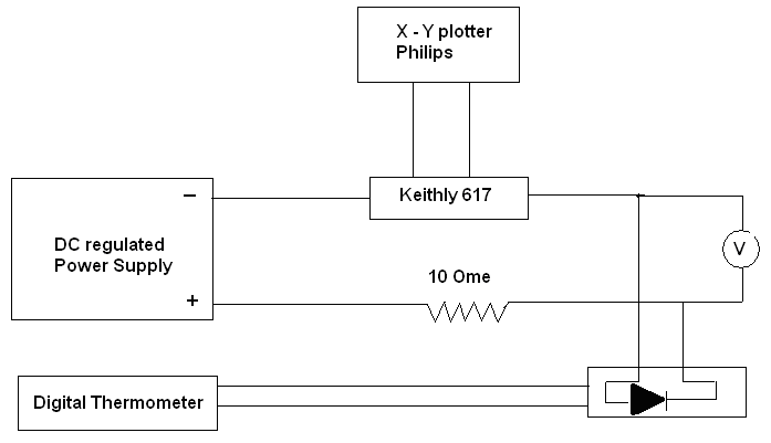 | Figure1. Circuit diagram for I-V measurements before and after irradiation |
4. Results and Discussion
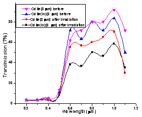 | Figure 2. Spectral transmission before and after the electron beam irradiation for CdSe(In) and CdSe at the same thickness 3µ m |
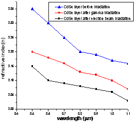 | Figure 3. CdSe spectral refractive index before and after gamma and electron beam irradiation |
| |||||||||||||||||||||||||||||||||||||||||||
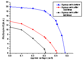
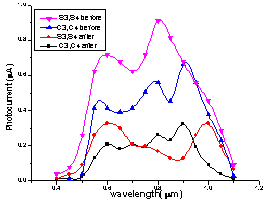 | Figure 4. Spectral response of (C3,C4) and (S3,S4) groups as a function of photocurrent before and after electron beam irradiation |
 | Figure 5. I-V characteristics for group (S) 3µ m before and after electron beam irradiation |
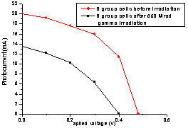 | Figure 6. I-V characteristics for groups 3 µ m before and after gamma irradiation |
5. Conclusions
- A n-CdSe/p-Si heterojunction solar cells with conversion efficiency 6% at AMI were fabricated by electron beam evaporation using single source of a stoichiomteric mixture of CdSe and In. The irradiation with gamma electrons beam with the same dose (650 Mrad) causes a degradation in the cells performance but still with better results than the conventional ones. The cell characteristics show a strong dependence on CdSe layer thickness and In: CdSe ratio before and after the irradiation. However better precautions and handling fabrication parameters theoretical optimization parameters theoretical optimization and applying other techniques such as antireflection coating and back surface field can improve the performance of the can n-CdSe/p-Si Heterojunction solar cells.
References
| [1] | A.F.W. Willoughby, "The control of Radiation Resistance in Space Solar Cell" Int.J.Electronics, 865,1974. |
| [2] | Masafumi Yamaguchi, Aurangzeb Khan, Nethaji Dharmarasu M. Yamaguchi "Analysis for superior radiation resistance of InP-basedsolar cells". Solar Energy Materials & Solar Cells 75 (2003) 285–291. |
| [3] | T.A.Cross, "Photovoltaic for Commercial Space Applications", Proceeding of the second World Renewable Energy Congress, Uk, 212, 1992. |
| [4] | Mostafa E. Moussaa, Mohamed Y. Fetehab, M.F.M. Hassanc" Gamma irradiated CdS(In)/p-Si heterojunction solar cell".Volume 23, Issues 3–4, July 2001, Pages 361–367. |
| [5] | N.ll.Karam, et.al., "High Efficiency Gain P2/GaAS/Ge Dual and Triple Junctions solar cells for Space Applications", Proceeding of the second World Conference on Photovoltaic Solar Energy Conversion, Austria,3534,1998. |
| [6] | R.J.Walters, "Diffusion Length and defect Studies in proton Irradiated Inp/Si Measurements", Proceeding of the second World Conference on Photovoltaic solar energy conversation, Austria,3550,1998. |
| [7] | T.llayashi,"P-Si/n-CdS Heterojunction Solar Cells", Jap.J. of Appl. Phys., 1174, 1989. |
| [8] | II.Okimura and R.Konodo,. Jap.J.of Appl.274,1970 . |
| [9] | R. B. Konda, R. Mundle, H. Mustafa, O. Bamiduro, A. K. Pradhan, U. N. Roy, Y. Cui, andA. Burger, "Surface plasmon excitation via Au nanoparticles inn-CdSe/p-Si heterojunction diodes", Appl. Phys. Lett. 91, 191111 (2007). |
| [10] | Lingzhi Du, Youan Lei , "Synthesis and photovoltaic characteristic of n-type CdSe nanobelts", Materials Letters 73 (2012) 95–98. |
| [11] | A. A. Elshazly. Et.al., "Electrical and optical Properties of Doped CdS thin Film", Proc. Of 12th National radio Science Conf., Egypt, 1995. |
| [12] | Jae-Hyeong Leea, Jun-Sin Yia, Kea-Joon Yangb, Joon-Hoon Parkc, Ryum-Duk Ohd "Electrical and optical properties of boron doped CdS thin films prepared by chemical bath deposition", Thin Solid Films 431 –432 (2003) 344–348. |
| [13] | Shadia J. Ikhmayies a, Riyad N.and Ahmad-Bitar," A Comparison between the Electrical and Optical Properties of CdS: In Thin Films for Two Doping Ratios", JJMIE ,Volume 4, Number 1, Jan. (2010), ISSN 1995-6665, Pages 111 – 116. |
| [14] | C. Couluzza et. Al., "n-CdS/p-Si Heterojunction Solar Cells ", Appl. Phys. Lett., 569, 1980. |
| [15] | Raid A. Ismailro, Abdul-Majeed E. Al-Samaf , Omar A. A.Sultan "p-cds/n-Si Anisotype Heterojunction solar cells With Efficiency of 6.4oh" . Qatar univ. Sci.J.(2005), 25: 31-39. |
| [16] | R. R. Arya, "Efficient Cadmium Sulphide on Silicon solar cells", Appl.Lett., 355 ,1982. |
| [17] | W.J. Danaher, L.E. Lyons, G.C. Morris, Sol. Energy Mater. 12 (1985) 137. |
| [18] | R. Swanepole and R.P. Wayne," principles and applications of photochemistry ". J.Phys. E:sci. Instrum., 16, oxford Uni. Press, UK, 1988. |
| [19] | M.El-Muradiel. Et. Al.," The Effect of Gamma Rays Radiation on Silicon Solar Cells"., Proc. Of Renewable Energy Congress, UK, 536, 1992. |
| [20] | M.A. Iqbal, and W. Awais, " The Effects of Gamma Radiation on Silicon Solar Panels".(2010) |
| [21] | M.ashry and S.fares "Diffusion Length Analysis and Measurement in the base region of photodiodes " J.Phys. and Chem. S 46, 2429-2431, UK,2003. |