-
Paper Information
- Next Paper
- Paper Submission
-
Journal Information
- About This Journal
- Editorial Board
- Current Issue
- Archive
- Author Guidelines
- Contact Us
Microelectronics and Solid State Electronics
2012; 1(3): 53-59
doi: 10.5923/j.msse.20120204.01
Macromodeling of Power VDMOSFET Transistor Incorporating Self-Heating Effect
 Abstract
 Reference
 Full-Text PDF
 Full-Text HTML
Messaadi Lotfi , Dibi Zohir
Department of Electrical and Electronic Engineering, Advanced Electronic Laboratory (LEA) University of Batna, Rue Chahid Mohamed Boukhlouf 05000 Batna, Algeria
Correspondence to: Messaadi Lotfi , Department of Electrical and Electronic Engineering, Advanced Electronic Laboratory (LEA) University of Batna, Rue Chahid Mohamed Boukhlouf 05000 Batna, Algeria.
| Email: |  |
Copyright © 2012 Scientific & Academic Publishing. All Rights Reserved.
Self heating model simulation of power electronic semiconductors is now required in accurate optimisation of power electronic circuits and systems. This requires accurate, but not too complex, self heating models of power semiconductors to be used in commercially available power electronic circuit simulators. Realization of one such self-heating model for power VDMOSFET in PSPICE 10.5 is described in the paper. Model consists of electrical and thermal part with interactive exchange of variables. Self-heating model and standard model was tested on unclamped inductive circuit.
Keywords: Power VDMOSFET, Device Modelling, Junction Temperature, Power Discrete Devices, Simulation, Spice, Unclamped Inductive Switching
Article Outline
1. Introduction
- Today, circuit simulators are standard tools in the development and optimization of electronic systems. However, simulation has until now been limited to electronic functions because, in the simulation models available today, temperature dependence can at best be taken into account by changing the static global temperature. Inpower-electronic systems in particular, the temperature is one of the critical parameters due to the fact that many properties of power semiconductors are very strongly temperature-dependent – following are some examples:1) A maximum junction temperature is specified for all semiconductor components[3],[8] which, when exceeded, can lead to destruction or permanent damage of the component. Even when temporary events such as avalanche or short-circuit conditions occur, it must be ensured that the maximum permissible junction temperature is not exceeded – a problem which is almost impossible to solve by conventional means, i.e. using a Zth-diagram.2) Within the safe operating range, the lifetime of semiconductor components is strongly affected by temperature fluctuations due to loading. Each change in temperature causes mechanical stress in the component which, in particular, affects solder and bond connections. Here it is not the absolute temperature which is decisive but the temperature cycling. As a rule of thumb it can be assumed that the aging of a as a rule of thumb it can be assumed that the aging of a component is proportional to the fourth (!) powerof the temperature deviation[1].3) The ON-resistance of a MOSFET and thus the conduction losses are roughly doubled with a temperature increase from 25℃ to 150℃.4) The threshold voltage of a MOSFET drops with increasing temperature which reduces the signal-to-noise margin at the control node. Ignoring this effect can lead to an undesired – even catastrophic – turn-on of the transistor when it should be inhibited, especially in bridge circuits with high slew rates for the drain-source voltage. In addition to these aspects, the question of the fluctuation in the junction temperature is also becoming more and more important in the course of circuit design. Some of the over dimensioning for example in the switching of lamps or motors to cover temporary overloads is no longer necessary when the brief, excessive power dissipation can be compensated by suitably coupled thermal capacitances. Similarly, this applies when one wants to do away with the usual protection circuits when relying on the high robustness of today’s power semiconductors. Avalanche energy of modern power MOSFETs for example is specified in such a way that any load current pulse pattern below the rated current is allowed as long as it is ensured that the peak junction temperature does not exceed the maximum value. In order to be able to simulate the time-dependent temperature curves which occur in all operating states, it is necessary to couple the electrical model of a component dynamically with the description of its thermal properties. For use in an electric circuit simulator, the thermal description by an electric analog model is to be preferred.The MOSFET model reference on which this work is based has been explained in[1]-[2]-[3]. The reader is encouraged to refer to these references for a full understanding of the MOSFET model parameters herein referred to as the standard SPICE MOSFET model. Recent works[8]-[9] have demonstrated methods of circumventing the SPICE global temperature definition, providing a means of using the device’s own junction temperature as a self-heating feedback mechanism.New model studied recently[10] has taken into account the statically behaviour. This paper presents a new version of the dynamical behaviour.
2. Standard SPICE MOSFET Model
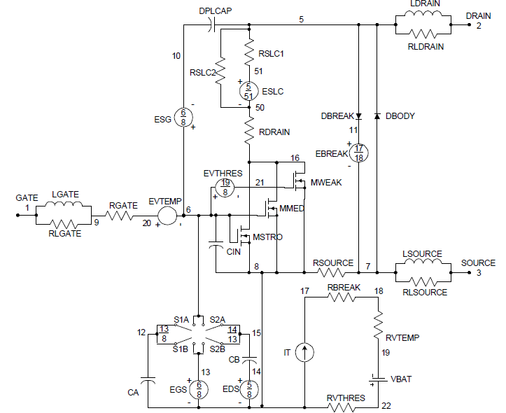 | Figure 1. Standard VDMOSFET Macro-model Dependent on Global Temperature Definition |
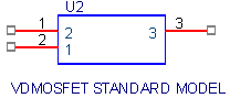 | Figure 2. Standard VDMOSFET PSPICE Symbol |
3. Self-Heating Spice MOSFET Model
- Improved implementation of static and dynamic behaviour is achieved with the self-heating SPICE MOSFET model (Figure 2), an evolution of the standard MOSFET model (Figure 1). Improved implementation of static and dynamic behaviour is achieved. Temperature dependent model parameters respond in closed loop form to the junction temperature information provided by node Tj. Performance is independent of SPICE’s global temperature definition .TEMP, circumventing the level-1 NMOS model primitive self-heating limitation. All MOSFET operating losses are inclusive in the current source G_Pdiss (scaling of 1A = 1W dissipation) representing instantaneous power dissipation into the thermal model.Multiple MOSFETs may be simulated at different and variable junction temperatures. Each MOSFET can be connected to a heat sink model via node Tcase. The heat sink model can be device specific, so heat sink optimization becomes possible. Current source G_Pdiss is referenced to the simulation ground reference, permitting use of the model in bridge topologies
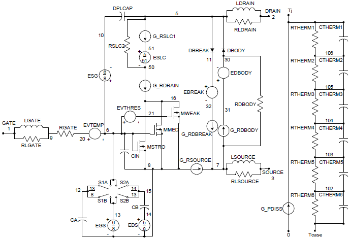 | Figure 3. Self-Heating VDMOSFET Macro-model Independent of Global Temperature Definition |
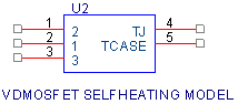 | Figure 4. Self-Heating VDMOSFET PSPICE Symbol |
4. Self-Heating model Implementation
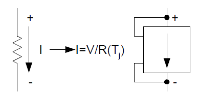
- Ability to describe the value of a resistor and its temperature coefficients as a behavioural model referenced to a voltage node is necessary to express dependence on junction temperature. SPICE resistor ABMs do not permit voltage node references. Dynamic temperature dependence of the MOSFET’s resistive element (expressed as separate lumped elements) and of the diode’s resistive component cannot be implemented without a resistor behavioural model. This limitation is overcome by using a voltage controlled current source ABM expression (Figure 5). By using the nodes of the current source for voltage control, it becomes possible to express a resistor as a voltage-controlled current source by implementing the expression for the resistor’s current as I = V/R (Tj). The resistance R (Tj) becomes a behavioural model expression dependent on the voltage node Tj representation of junction temperature. This voltage-controlled current source ABM model was used to modify the standard MOSFET model from Figure 1 by implementing voltage dependent versions of RDRAIN, RSOURCE, and RSLC1. Behavioural expressions were implemented in the self-heating model to eliminate IT, RBREAK, RVTEMP, and VBAT through modification of EVTEMP, EVTHRES, and EBREAK.
 | Figure 5. Implementing a Voltage Dependent ABM Resistor Model |
 | (1) |
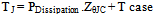
5. Simulating Unclamped Inductive Switching
- The unclamped inductive switching (UIS) test circuit in Figure 6 was used to compare the performance of the VDMOSFET (3.5 mΩ, 60V, TO-263) self-heating MOSFET model with that of the standard model and measurement results.
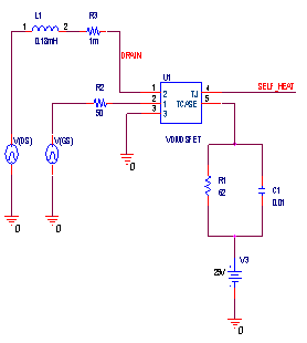 | Figure 6. UIS circuit used in the simulation |
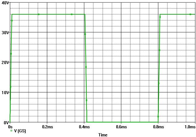 | Figure 7. Waveform of the gate voltage VG (V) |
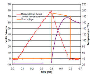 | Figure 8. Measured UIS waveforms for a VDMOSFET standard model |
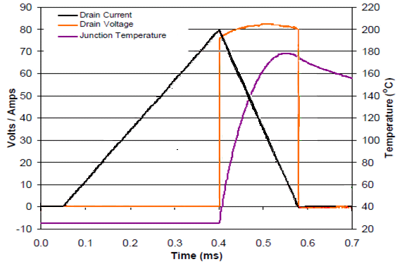
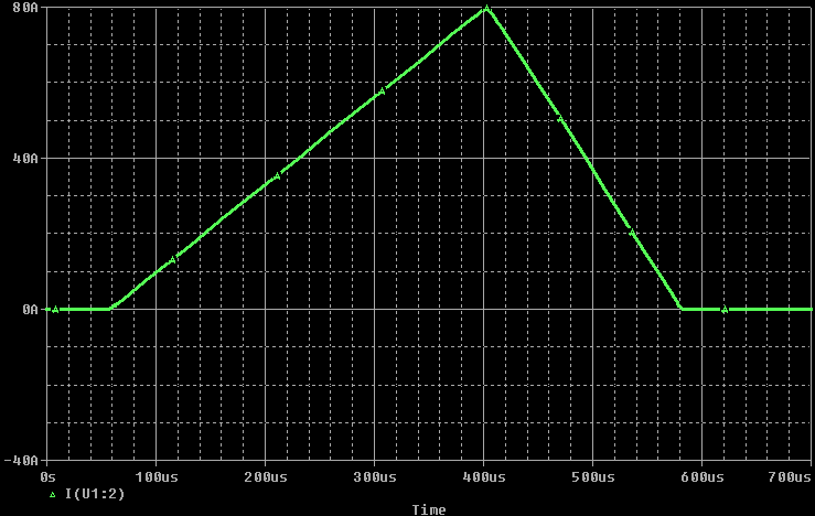 | Figure 8a. Simulated drain current (IDRAIN) for the VDMOSFET transistor |
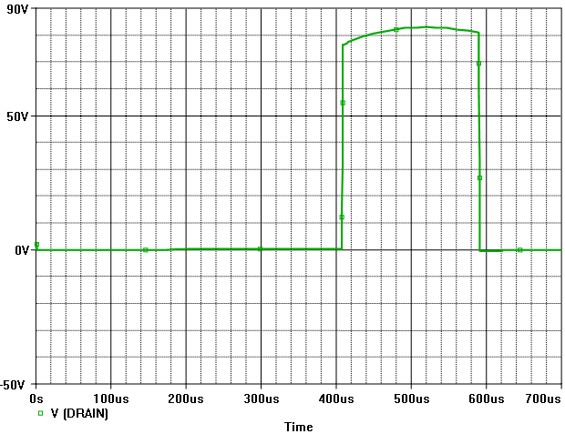
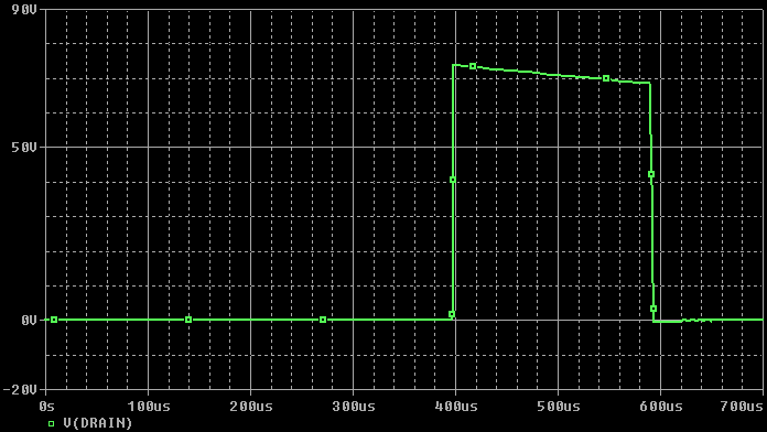 | Figure 8b. Simulated drain voltage (VDS) for the VDMOSFET transistor |
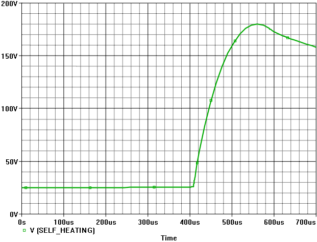
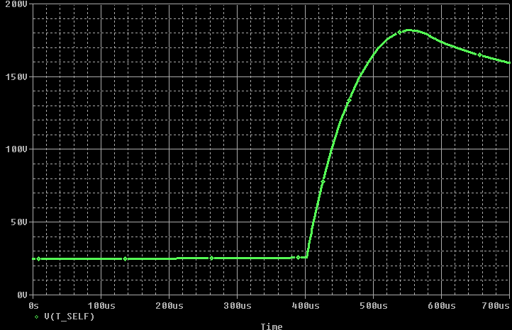 | Figure 8c. Simulated junction temperature (VSELF-HEATING) (1V=1℃) |
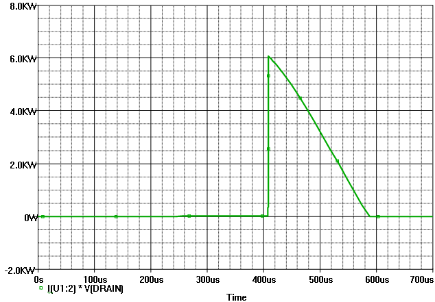
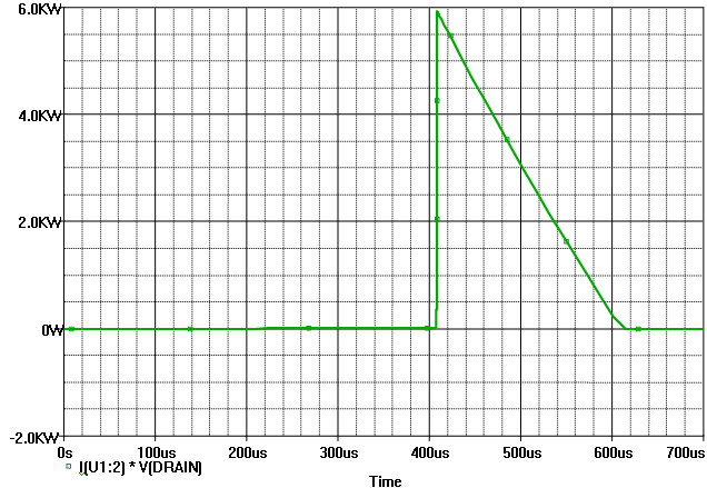 | Figure 8d. Simulated power loss (IDRAIN*VDRAIN) of the VDMOSFET standard model |
 | Figure 9. Measured UIS waveforms for a VDMOSFET Self-Heating Model |
 | Figure 9a. imulated drain current for the VDMOSFET transistor |
 | Figure 9b. Simulated drain Voltage (VDS) for the VDMOSFET transistor with self heating effect |
 | Figure 9c. Simulated Junction temperature (VSELF-HEATING) for VDMOSFET transistor |
 | Figure 9d. Simulated power loss (VDS*IDS) of the VDMOSFET self-heating model |
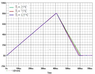 | Figure 10a. Simulated drain current (IDrain) at 25℃, 75℃ and 175℃ of VDMOSFET self-heating model |
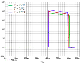 | Figure 10b. Simulated drain voltage (VDrain) at 25°C, 75℃ and 175℃ of VDMOSFET self-heating model |
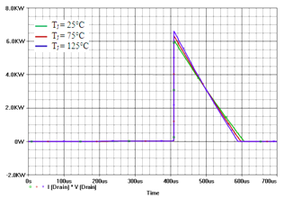 | Figure 10c. Simulated power loss (IDrain* VDrain) at 25 ℃, 75℃ and 175 ℃ of VDMOSFET self heating model |
6. Junction Temperature Dependency Analysis
- Switching behaviour of the VDMOSFET self heating model was tested over junction temperature to show the temperature dependency. Transient comparisons between experiment and simulation were presented at 25℃, 75℃ and 125℃. To observe more clearly the changes associated with temperature, experiment and simulation waveforms are shown in different figures as follows.
7. Simulation Convergence
- Many power electronics convergence problems can be solved with two option parameters, Gmin and Rshunt. The Gmin option is available in all PSPICE 9.2 and 10.5 programs. Setting the value of Abstol to 1u will help in the case of circuits that have currents which are larger than several amps. Setting Abstol to a value which is greater than 1u will cause more convergence problems than it will solve. UIS simulations were performed on a Dell Latitude CSx using a 3.8GHz Pentium IV processor with 1GB of memory. Windows XP was the operating system used (virus scan software enabled). PSPICE Schematics version 10.5 was usedSimulation time results were:- Standard model = 7.9s- Self-heating model = 13.7sSimulation time is expected to be longer with the self-heating model due to the dynamic interaction of the junction temperature feedback.
8. Conclusions
- An idea of the self heating PSPICE power MOSFET macromodel is described. We have added a simple ladder network model of MOSFET's thermal behaviour. Such a model can be successfully used in most standard electrical circuit simulators for determining semiconductor's operating temperature during various operation cycles domain simulations. In the second part of this paper we examined the unclamped inductive switching behaviour of standard and self heating VDMOSFET model. Good agreement of simulated results confirms the expectations.