-
Paper Information
- Previous Paper
- Paper Submission
-
Journal Information
- About This Journal
- Editorial Board
- Current Issue
- Archive
- Author Guidelines
- Contact Us
Microelectronics and Solid State Electronics
p-ISSN: 2324-643X e-ISSN: 2324-6456
2012; 1(5): 118-147
doi: 10.5923/j.msse.20120105.03
Yet Another Hydrodynamic Model with Correlated Parameters for Silicon Devices
 Abstract
 Reference
 Full-Text PDF
 Full-Text HTML
Muhammad H. El-Saba
Ain-Shams University, Faculty of Engineering, Dept of Electronic Engineering, Cairo, Egypt
Correspondence to: Muhammad H. El-Saba, Ain-Shams University, Faculty of Engineering, Dept of Electronic Engineering, Cairo, Egypt.
| Email: |  |
Copyright © 2012 Scientific & Academic Publishing. All Rights Reserved.
In this paper we present a complete hydrodynamic model (HDM) describing the transport of charge carriers in semiconductor devices with arbitrary band structure. The model is appended with advanced physical models for almost all the physical parameters of interest in modern Si Devices. These parameters are inter-related via the carrier energy relaxation time. An improved analytical model of the carrier heat flux, on the basis of a fourth moment of the Boltzmann transport equation (BTE), is also presented. In order to resolve the heat evacuation problems in SOI and power devices, the model is coupled with a lattice heat conservation equation. The transport of hot carriers is simulated, according to the proposed HDM and the results are compared with the conventional data obtained using the drift-diffusion model (DDM) and MC simulation. We show from the HD simulation, the effect of the energy relaxation time value on the hot carrier transport in general and the breakdown voltage in particular, of both MOSFETs and bipolar devices.
Keywords: Semiconductor Devices, Hydrodynamic Modelling, Simulation, Semiclssical transport theory, Impact Ionization, Injection, Hot carriers
Cite this paper: Muhammad H. El-Saba, "Yet Another Hydrodynamic Model with Correlated Parameters for Silicon Devices", Microelectronics and Solid State Electronics, Vol. 1 No. 5, 2012, pp. 118-147. doi: 10.5923/j.msse.20120105.03.
Article Outline
1. Introduction
- For a gas of charge carriers of q-type, where q stands for (n) for electrons or (p) for holes, the semiclassical Boltzmann transport equation (BTE) may be written as follows, when charge carriers are not strongly correlated [1]
 | (1.a) |
 ) and ultra fast devices (working up to the terahertz range) has been lately a subject of debate, we just remind here the main assumptions on which the BTE in semiconductors is based [2].● Collisions are localized in space, so that the mean free path of charge carriers is much greater than the de-Brouglie wavelength,● Collisions are instantaneous in time such that the collision time is much smaller than the time between subsequent collisions,● External electric field force does not vary greatly over small distances in the order of wave packet length,● Particles are weakly correlated (Bogoliubov assumption [3]) and the many body effect is negligible. Mathematically speaking, the BTE is valid as long as the following Barker condition is realized [4]:
 | (1.b) |
 is the maximum applied electric field, m* is the carrier effective mass,
  is collision time and
  is mean free time between collisions and q = k–k’ is the wave vector of (emitted or absorbed) phonons during collisions.For strongly ionized gasses and degenerate semiconductors, where particle-particle collisions are not negligible, the Boltzmann transport equation may be replaced by the Fokker-Planck equation [5-6]. For ultra small devices, whose active layers dimensions (at least one of them) are in the order of De Broglie wavelength, the BTE should be replaced by one of the quantum transport formulations [7-11], like the Wigner-Boltzmann transport equation (WBTE) [9-11]. However, there exist several approaches to include the degeneracy effects and quantum corrections to the semiclassical transport models (e.g., [12-13]). The solution of semiclassical BTE is carried out by a variety of methods [14-26], among which the iterative methods [15], the matrix methods [16], the Monte Carlo method [17-21], the cellular automata method [22], truncated expansion (usually in Legendre polynomials and spherical harmonics) methods [23-26]. In addition, the so-called energy transport model (ETM) and moment methods [27], which are sometimes called the hydrodynamic model (HDM), have been also used to solve the BTE in the hot carrier regime. In the ETM approach the distribution function is decomposed into an even and odd parts and the collision term is expressed using a microscopic relaxation time approximation [28].The hydrodynamic description of the gas of charge carrier in semiconductors consists in the study of the evolution of certain macroscopic quantities, whose physical meaning is significant and whose quantity is eventually measurable. So, the HDM is constructed by multiplying the semiclassical BTE with a number of weight functions and integrating these equations over the phase or momentum space, so that a set of differential equations in physical space and time is obtained. This method is hence an averaging process that leads to the loss of some microscopic information in the distribution function. However, in many practical cases the resultant average (or macroscopic) parameters retained by the equations in the physical space are sufficient to capture the essential features of the carrier transport phenomena. The HDM has been widely used in the study of aerodynamic flow, and was suggested to study the hot electron transport in multivalley semiconductor devices by Bløtekjaer [29]. Since then, several contributions have been introduced to improve the hot carrier transport models in semiconductors and the HDM in particular [30-47]. For instance, the nonparabolicity of energy bands has been included in the HDM for the first time by Thoma et al [38]. The energy transport model ETM was reformulated by Chen, Kan and Ravaioli, who assumed non-Maxwellian and nonparabolicity correction factors, to solve the contradiction involved in evaluating a non-zero heat flux term for a Maxwellian distribution [39]. Also, the number of considered moments in the HDM has been increased in order to improve the HDM accuracy [44]. Unfortunately, all the added improvements to the HDM were associated with the addition of a huge number of new physical parameters [45-46]. On the other hand, some authors neglected the role of some important parameters in order to reduce the complexity of the model. This led to several paradoxal results and the failure of the HDM, in certain situations [47]. We try here to generalize the previously introduced models while reducing the number of physical parameters, by correlating them all to the energy relaxation time. We start by introducing the system of hydrodynamic equations in section II. In section III we discuss the system closure hypotheses. We present the physical definition of the carrier temperature. In section IV we present an almost complete description of the physical parameters in the bulk of semiconductor devices. Finally we present our conclusions in section VIII.
2. System of Hydrodynamic Equations
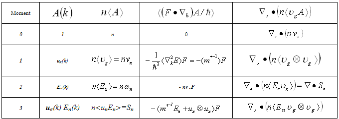
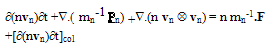
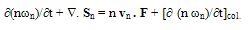
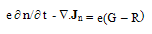
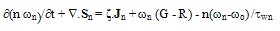
- The multiplying weight functions in the HDM for semiconductors are usually chosen as powers of increasing order of the carrier vector kq, or carrier group velocity uq, or even the carrier momentum pq. The powers of these parameters are usually formatted using some appropriate scaling factors to get physically meaningful quantities. For instance, if we adopt the powers of the carrier group velocity as weight functions (e.g., 1, uq and uq2), then we use the carrier energy Eq = ½mq*uq2, instead of uq2 as the second-order multiplier. So, the set of conservation equations of carrier concentration, momentum and energy may be obtained by multiplying the BTE by the first powers of the carrier group velocity uq (e.g., 1, uq and Eq), and then integrating the two sides of the resulting equations over the whole k-space (see Appendix I). For the sake of simplicity and brevity we write here only the electron equations in a single-valley semiconductor. In multi-valley semiconductors, we may assume a single lumped valley or write similar equations for each valley of the semiconductor [37]. The electron density-, momentum- and energy- conservation equations, in a semiconductor, can be put in the following form:
 | (2.a) |
 | (2.b) |
 | (2.c) |
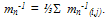 At the bottom of conduction band the average mass will be denoted by mno and its value in Si , according to optical measurements is about 0.275 mo. The subscript ‘col.’ In the above equations means the rate of change of the quantity between brackets due to electron gas collisions with the semiconductor crystal lattice and its defects. The sign
  stands for the tensorial product of two terms such that:
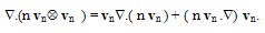 | (3.a) |
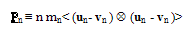 | (3.b) |
 | (4.a) |
 | (4.b) |
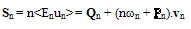
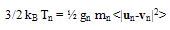
 | (5.a) |
 is the mass density of the gas. In the ideal gaz theory, the gaz mass density is a macroscopic quantity and
  is taken outside the averaging brackets. So, the gas mass density is given by:
 | (5.b) |
 Hence, our definition of the gas pressure, Pn, is different from the classic definition of electron gas pressure tensor, Pn:
  | (5.c) |
 | (5.d) |
 is the edge of the conduction band. Similarly, the applied force on holes is F=∇Ev, where
  and Evo being the edge of the valence band. The electrostatic potential distribution can be found by solving the Poisson equation:
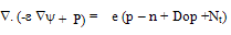 | (6) |
3. Closing the System of Hydrodynamic Equations
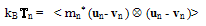
- In order to close the system of conservation equations for charge carrier density, average momentum and average energy (2-a,b,c) we usually adopt some assumptions to approximate the terms which depend on the knowledge of the distribution function. The main assumptions are usually concerned with the following items:1. definition of the carrier gas pressure and temperature,2. approximation of collision terms, 3. modeling the heat flux term (the third center moment of the distribution function), and4. modeling any other higher moment terms, if the number of moments is greater than 3.When the kinetic pressure of the gas of electrons is considered as a scalar quantity, one can define the electron gas temperature, Tn, by the law of perfect gases Pn = n kB This assumption does not imply a spherically-symmetric distribution function about its mean value in the momentum space (like the displaced Maxwellian distribution). Equation (5-a) can be merged with the hypothesis of the perfect gas law, in one relation defining the electron gas temperature as follows:
 | (7) |
 | (8) |
 the eventual error due the effective mass approximation is absorbed in the gas pressure correction factor, which can be calculated by MC simulation. However, it is well known that the convection part of the the average electron energy is generally small compared the thermal part, except for device regions where the velocity overshoot is pronounced.As for the collision terms, we make use of the macroscopic relaxation time approximation [31]. In this approximation, the collision term in the momentum conservation equation is expressed in terms of a macroscopic momentum relaxation time
  as follows:
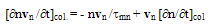 | (9.a) |
 as follows:
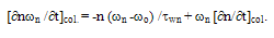 | (9.b) |
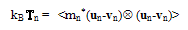
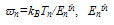
 is the electron energy at thermal equilibrium and TL is the lattice temperature. Note that the collision term in the above two equations is decomposed into two terms. So, the momentum and energy relaxation times, include the effect of collisions over optical while the effect of impact ionization collisions is included in the [∂n/∂t]col. The collision term [∂n/∂t]col., which appears explicitly in the carrier density conservation equation can be expressed as follows:
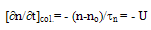 | (9.c) |
 | (10.a) |
 | (10.b) |
 | (10.c) |
 is defined as follows:
 | (11.a) |
 is measured above the conduction band edge Ec, while the average hole energy
  is measured under the valence band edge Ev. In steady state (up to the terahertz frequency range), the carrier momentum conservation equations can be further simplified by suppressing the partial time-derivatives so that:
 | (11.b) |
 | (11.c) |
 | (11.d) |
 | (11.e) |
 | (12.a) |
 | (12.b) |
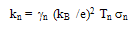
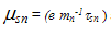
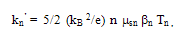
 is the electrical conductivity and
  is the Lorenz number (for electrons). In the original Wiedeman-Franz formulation (using the microscopic relaxation time approximation)
  is given by:
 | (12.c) |
 expression, which is given by:
 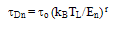 | (12.d) |
4. About the Definition of the Carrier Temperature
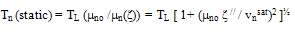
- In this section we compare the different approaches for modeling the carrier temperature. Formally, temperature is a property which governs the transfer of thermal energy, or heat, between one system and another. The electronic temperature concept was initially introduced in 1947 by Fröhlich [52], and since then it has been exploited by several authors to model the high-field transport in semiconductors. In the isothermal drift-diffusion model (DDM), the carriers temperature is assumed equal to the lattice temperature TL. However, the so-called static electron temperature Tn may be roughly estimated from the electric field distribution in several ways [53]. For instance, the static temperature may be defined as follows:
 | (13) |
 is the electron drift mobility, vnsat is the electron saturation velocity and
 is the low-field drift mobility. Also, ζ// is the parallel component of the electric field to the electron current density such that ζ // = ζ .Jn/|Jn|. The above equation is based on the assumption that the parallel component of the diffusion coefficient is almost constant and independt of the electric field [33]. Such static forms of the carrier temperature exclude the lag effect between the electric field and the carrier temperature, and hence the velocity overshoot phenomenon will not be observed. However, the definition of the carrier temperature in the simulation is given by:
 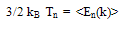 | (14.a) |
 | (14.b) |
 | (15.a) |
 | (15.b) |
 such that:
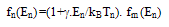 | (16.a) |
 | (16.b) |
 | (17.a) |
 | (17.b) |
 | (17.c) |
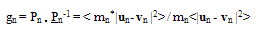
 | Figure 1. Electron temperature according to MC [29], classic HDM and our model |
 | (17.d) |
5. Energy-Dependent Physical Parameters
- The accurate modelling of transport parameters, as the carrier drift mobility and impact ionization rate at high energies, is vital in any transport model. In the DDM, these parameters were usually expressed as functions of the local electric field [54-55]. Nevertheless, we know that these parameters express physical mechanisms involving energy exchange and should be expressed as functions of the carrier energy, rather than the local electric field. Fortunately, the solution of the HDM produces such information about the carrier energy distribution and permits to express these parameters in a physical manner, along the semiconductor device. In the following subsections, we discuss the modelling of the energy-dependent physical parameters in the bulk of silicon devices.
5.1. Carrier Drift Mobility
5.1.1. Carrier Drift Mobility in the Bulk:
- In the drift-diffusion model, the high-field drift mobility in the bulk of a semiconductor is usually expressed by the Caughey-Thomas model, in its scaled form [56]:
 | (18.a) |
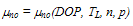 is the low-field mobility of electrons, which is related to doping, temperature and injection level, and may be expressed by a suitable model, e.g., Dorkel-Leturcq [57] or Klassen [58] models. Also vnsat is the electron saturation velocity and may be expressed by the model of Canali et al. [59]:
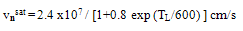 | (18.b) |
 The energy-dependent drift mobility relation may be written in the following form [60]:
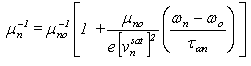 | (18.c) |
 is taken from MC simulation, as shown in Figure 4(a). In order to compare our model with the field-dependent phenomenological relations, one can substitute equation (18-b) into the set of HDE’s in steady state homogeneous case to obtain:
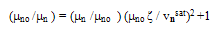 | (19.a) |
 | (19.b) |
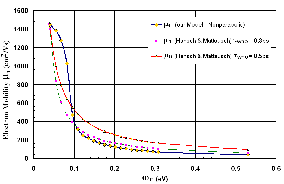 | Figure 2(a). Electron drift mobility in Si at 300K versus electron temperature, according to the model of Hänsch-Mattausch with different values of  [43] and according to our model [43] and according to our model |
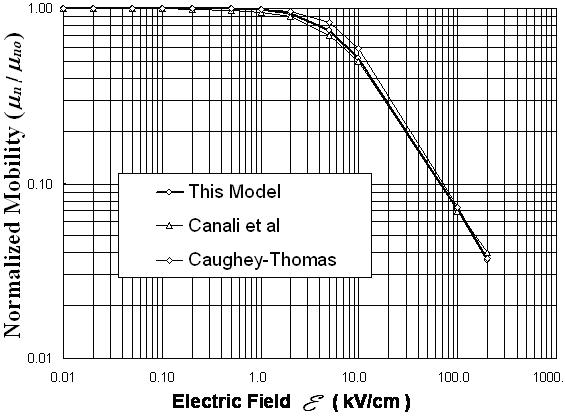 | Figure 2(b). Electron drift mobility in Si at 300K, according to Canali et al [56], Caughey-Thomas model [52] and our model |
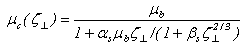
5.1.2. Carrier Drift Mobility near the Surface
- The drift mobility near the surface of a semiconductor is greatly reduced because of the additional scattering mechanisms due to the rupture of crystal periodicity, the surface phonons, the surface roughness and the eventual presence interface states. In addition, the presence of confined electrons into a thin layer near the surface of MOSFETs (the inversion layer) gives rise to quantization effects (subbands). As suggested by Sabins and Clemens [64], the reduction in the effective surface mobility may be expressed as a unique function of the effective vertical field ζ┴. The most famous model of the surface mobility in MOSFET devices has been, for long time, the Yamaguchi model [65]:
 | (20) |
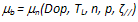 is the bulk drift mobility. According to Hänsch-Mattausch model [61], the drift mobility along the semiconductor surface is given by the following relation:
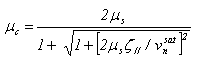 | (21.a) |
 replaced with the reduced surface mobility
  which is given by:
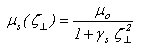 | (21.b) |
 are constants. In fact, the channel mobility can be modeled by the Schwarz empirical formula, when we neglect the effect of generated surface states [66]:
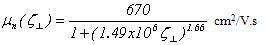 | (21.c) |
 | (21.d) |
 are constants. The effective vertical field ζ┴ is sometimes related to the surface potential and may be approximated by the following relation, for MOSFETs wih n+ polysilicon gate under strong inversion conditions [68]:
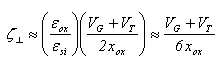 | (22) |
 are the dielectric constants of silicon and gate oxide, and xox are the MOSFET gate voltage, threshold voltage and gate oxide thickness, respectively.A more elaborate and universal field-dependent mobility model, which reproduces the measured mobility data of Takagi et al. [69] at the surface of semiconductor devices is given by Darwish et al. [70]. According to Darwish’s model, the total carrier mobility is expressed by an equation similar to the scaled Hansch-Murrata model (21.a), with
  is given by:
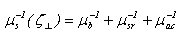 | (23.a) |
 is again the bulk mobility,
  is the carrier mobility limited by surface roughness and
  is the carrier mobility limited by surface acoustic phonons. In the later model, the bulk mobility,
  is expressed by the klassen model [58], the surface acoustic,
  , follows the Lombardi model [71]:
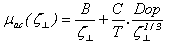 | (23.b) |
 is given by:
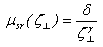 | (23.c) |
 are constants, depending on the technology
  for electrons and 4.1x10¹⁵ V/cm for holes,
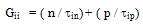
5.2. Impact Ionization Rate
- The generation by impact ionization is one of the most important mechanisms limiting the performance of semiconductor devices in general and the submicron MOSFETs in particular. In fact, the electron-hole pair generation by impact ionization, Gii , influences so many characteristics of semiconductor devices such as the breakdown voltage and hot carrier injection currents. The impact ionization mechanism was identified, about 50 years ago, by McKay [72]. Since then, the literature of the impact ionization mechanism has been extensive, e.g. [73-108], but only a few reviews are available. The generation rate by impact ionization Gii has been always expressed in terms of Townsend coefficients (or ionization rates of electrons and holes),
 as follows:
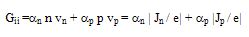 | (24.a) |
 | (24.b) |
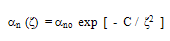
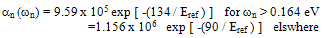
 and C are constants. According to Baraff [74], this procedure is only justifiable at very high electric fields where electron-phonon collisions are frequent and the momentum distribution function is isotropic. Also, Keldish [75] solved analytically the BTE at high energy assuming parabolic band structure and calculated the impact ionization rate using the symmetric part of the distribution function. The Keldish solution attracted the attention because it tends to the Wolff relation (exp[-C/ζ2]) at high fields and tends to a simple exponential exp[-C’/|ζ|] (where C’ is another constant) at moderate fields, which coincides with the experiment. In fact, the measurements of Chynoweth [74], Lee et al [77], Van Overstraten and Deman [78], Kotani and Kawazu [79], Maes [80] and Takayangi [81] showed that the impact ionization rate at moderate fields follow a simple exponential function. According to Grant’s model [82], the electron impact ionization rate follows the following exponential relation:
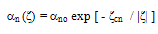 | (24.c) |
 | (24.d) |
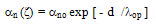
 is the mean free path between collisions with optical phonons. This model has been utilized to describe the breakdown phenomenon as well as the hot carrier injection and leakage currents in MOSFET devices in DDM-based simulation for long time [84-85]. Unfortunately, the parameters of the lucky-electron exponential model are dispersed among the different measurements of different authors in the literature [84]. In fact, the impact ionization phenomenon happens when drifting electrons have enough energy to ionize the valence electrons of lattice atoms. As the electron energy depends on the whole path of the electron under the effect of both the electric field and collisions, the local electric field value cannot directly reflect the real value of its energy. Thus, the local electric field dependent models of the impact ionization are not physically adequate, and their success in certain classic cases is due to their adjustable parameters. However, with the advent of the hydrodynamic model for semiconductors, where the carrier energy distribution is available, several authors tried to express the impact ionization rates in terms of the carrier mean energy or temperature.
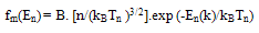
5.2.1. Schöll-Quade Impact Ionization Model
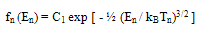
- The model of Schöll and Quade [87-88] for imact ionization rate is based on the heated Maxwellian approximation for the symmetric part of the distribution function. According to this model, the impact ionization rate of electrons is given by:
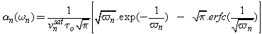 | (25) |
 is the electron ionization threshold energy,
 is a constant
  and erfc(x) is the complementary error function. Note that this model considers a parabolic energy band (constant effective mass mn*). In order to get adequate results at moderate fields, both Enth and
  are usually considered as adjustable parameters, with values which are extremely far from their physical meaning. For instance, Souissi et al [89] considered Enth ≈ 4eV and
  in order to fit this model with experiment.
 5.2.2. Baccarani & Stork Impact Ionization Model
- The model of Baccarani and Stork belongs to the category of semi-empirical models, which are based on the Shockley lucky-electron model. According to Baccarani and Stork [90], the rate of impact ionization is given by:
 | (26) |
 are constants. According to Baccarani and Stork, the ionization threshold energy Enth =1.1eV, the energy relaxation length
  the mean free path between opical phono collisions
  and the adjustable parameter c is equal to 2x1012 cm-2. However, Souissi et al. [89] used the model of Baccarani and Stork in their investigation about impact ionization in bipolar transistors and found that the best fit with measured values implies Enth=5.077eV. It has been shown in the latter work that both the Schöll-Quade and Baccarani-Stork models may be used to predict the multiplication factor
  across the base-collector zone with reasonable error, only over a limited range of applied bias.
5.2.3. Non-Maxwellian Distribution Function–based Impact Ionization Models
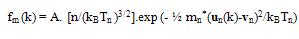
- In order to get rid of the disadvantages of the above mentioned models, some authors tried to calculate the impact ionization rate as a function of carrier energy, starting from its microscopic definition, on the basis of non-Maxwellian distribution functions [91-98]. For instance, Matsuzawa, Komahara and Wada [90] suggested the following form for the hot carrier tail of electrons distribution function:
 | (27.a) |
 | (27.b) |
 | (28) |
5.2.4. Advanced Impact Ionization Model
- Unfortunately, the success of the above mentioned energy-dependent models of impact ionization is limited to specific cases at small and moderate fields. In addition, these models make use of a number of adjustable parameters, whose fitting values have sometimes irrelevant physical meaning. We think that one source of errors is their lake to a link with the realistic band structure of the semiconductor material. The following phenomenological model accounts for the energy band structure and can be used, with no need to curve fitting of its physical parameters [102].
 | (29.a) |
 are the electron and hole average ionisation rates. Starting from the scaled form of the impact ionization rate, according to the Thornber theory [103]:
  | (29.b) |
 are the critical fields at which the electrons surmount acoustic phonons, optical phonons and impact ionization scattering thresholds. Assuming that the ionization rate can be fully described by the kinetic moments
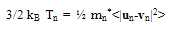
  one can write the energy conservation equation (10-c) in the following form in static field conditions:
 | (29.c) |
 being the electrons lifetime and no is the equilibrium electron density) and the third term represents the loss of electron energy due to collisions with optical phonons. The second term may be dropped from the above equation because
 . Also the the first and third terms can be combined, with an effective energy relaxation time, which includes the effect of impact ionization at high energies. In fact, this effect is not significant, according to Schöll and Quade [88]. Substituting the product eζ.vn from (27-c) into (27-b), we get the following expression for the electron ionization rate at moderate and high fields:
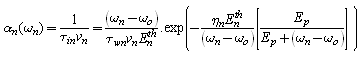 | (30.a) |
 is the electron mean free path between optical phonon collisions and Ep is the mean optical phonon energy. At low and moderate fields, this model can be approximated to the following simple form:
 | (30.b) |
 is the asymptotic value of impact ionization rate and
 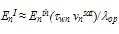 is the mean ionization threshold energy for electrons. However, at high fields the impact ionization rate is proportional to
 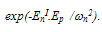 Note that we consider
  and
and  So, even at low fields the exponential realation
  does not imply a Maxwellian distribution because EnI is energy dependent. The energy dependence of the energy relaxation time, which implicitly includes the energy band structure effects, can be obtained from MC simulation or by measurement as indicated in the next section IV-C. Unlike classical models, the hard threshold energy (Enth) is replaced with a soft (energy-dependent) mean threshold energy (EnI) in our model. This coincides with Bude and Hess conclusions about the impact ionization soft threshold [102]. The calculation of
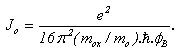
  as a function of the electron energy may be carried out by MC simulation in the bulk, using the relation [105]:
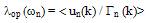 | (31.a) |
 is the total scattering rate by optical phonons. It may be also estimated from the so-called lucky-electron exponential model LE-EM [86]. In our analysis we used the following phenomenological relation, which is based on Crowell and Sze model [106], at the carrier temperature:
 | (31.b) |
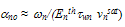
 is mean free path between collisions at low fields (when Tn ≈TL). Figs. 3(a) and (b) depict the variation of
  in Si, according to the above relations. In our calculations, we took Ep = 60meV and
  and exponentially extrapolated the available MC data of
  as shown in figure 4(a). For the matter of comparison, we plotted
  according to Baccarani-Stork and Scholl-Quade models, beside our model. The Scholl-Quad model produces exceesively high rates when the physical value of
  is taken into account. So, we set
  equal to 12.6fs, about 3 orders of magnitude greater than its physical value [86]. Note that the value of
  in our scaled model is greater than all other models and continues to increase at high energies. In fact, the experimental values of
  may exceed 106 cm-1. For instance, the measurement of Kotani and Kawazu of
  is usually fitted with
  cm-1 [79]. Also, the homogeneous MC simulation [105], indicates that the impact ionization pre-exponential is almost 106 cm-1 at high energies, as depicted by equation (26). It worth noting that the impact ionization rate at high energies (in the saturation region) is greatly influenced by the roll-off of the enrgy relaxation time, while Enth and
 have a relative influence at low and medium energies. This explains the failure of the previously suggested models, to properly estimate
  at high energies, even with adjusting Enth and the pre-exponential factors with non physical values, while fixing both
  For the matter of verification, Figure 14 depicts the I-V characteristics of a reverse biased p-i-n diode near avalanche, with different transport approaches (the DDM, the classic HDM with Scholl-Quade model and our proposed HDM model). As shown, the I-V characteristics obtained by our model are softer and the breakdown voltage is smaller and more realistic than the classic HDM results.
 | Figure 3(a). Electron mean free path between optical phonon collisions in Si at 300K, according to the lucky-electron exponential model (LE-EM), after [69], and according to the Crowel-Sze model [85] at the electronic temperature |
 | Figure 3(b). Electron impact ionization rate in Si at 300K, as a function of average electron energy, according to Baccarani-Stork model   Scholl-Quade model Scholl-Quade model  In all models In all models  |
 | Figure 3 (c). Average ionization energy in Si at 300K, according to our model model  |
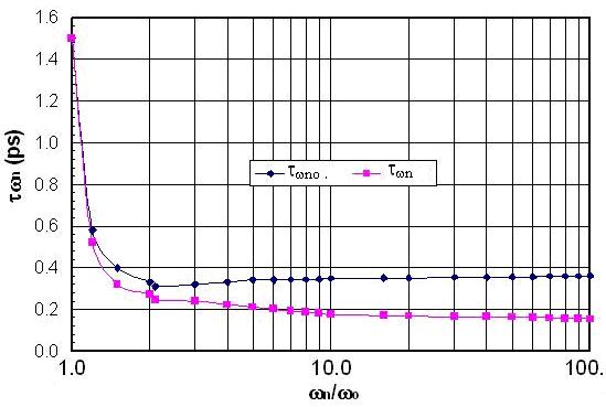 | Figure 4(a). Variation of the electron energy relaxation time with electron average energy in Si at 300K, according to MC simulation. In the above curve, the energy bands are assumed parabolic. The lower curve takes the non-parabolicity of the conduction band into account (non-parabolicty factor 0.5V-1) |
 | Figure 4 (b). Experimental value of electron and holes conductivity mass, after Rife [95] |
5.2.5. Energy Broadening of Impact Ionization Threshold
- The determination of the impact ionization threshold has been a subject of extensive research, both theoretically and experimentally [107]. In fact the measured values of the ionization threshold and those used in the theoretical models vary widely. As we pointed out in the last section, the mean ionization energy EnI in our model of impact ionization has a soft distribution around Enth. In order to evaluate the broadening of mean ionization energy, we define
 as follows:
 | (32) |
 as a function of mean electron energy. This broadening is mainly due to the variation of the energy relaxation time and the mean free path at high energies. Curiously, one may wonder if there is any reason to relate this phenomenon with the broadening in energy levels due to finite lifetime of energy states between scattering events at high energy [108-109]. In fact, it has been shown experimentally in [110] that there exists a line broadening transition, representing the transition from phonon scattering dominated to impact ionization dominated transport not only in silicon but also in any material with a bandgap. In addition, some theoretical studies of the impact ionization on the basis of quantum transport showed that a fixed impact-ionization threshold does not exist, and the impact-ionization scattering rate is drastically enhanced around the semiclassical threshold by the intracollisional field effect [111]. Of course, the broadening factor may be better evaluated by precise MC simulation, taking into account the impact ionization mechanism. However, with our simple model of
 and the exponentially extrapolated
  we found that
  is centralized around a minimum (almost zero) at
  , which is interestingly equal to 3/2 Enth. It should be noted here that we chose Enth= Eg ≈ 1.2 and chose o.= 1000Å, such that the distribution of
  is as close as possible from the experimental LE-EM curve. As shown in figure 3(a), the two curves almost intersect at
  =1.2eV.
5.3. Carrier Energy Relaxation Time
- The choice of the energy relaxation time is crucial in the HD simulation because it influences both the static and dynamic characteristics of the device to be simulated. According to the hydrodynamic theory, the exact modelling of the carrier energy relaxation time (and all other relaxation times) should be expressed as function of all the carrier moments like
 [112]. However, as we usually truncate the series of moments and satisfy ourselves with the few first moments, it is believed that much of the information about the energy relaxation time is related to the carrier mean energy and density [30]. According to Jacoboni and Reggiani [112], the energy relaxation time should decrease at high fields in a phenomenological way representing the tendency of the isotropic part of the distribution function to decay towards its equilibrium value. So, the later authors used the following equation, to evaluate the carrier energy relaxation time for warm electrons:
 | (33.a) |
 | (33.b) |
 from MC simulation [115]. Gonzalez et al. employed this relation to calculate the fitting parameters of their energy relaxation time model [116]. On the other hand, several authors considered the energy relaxation time as a constant when the electron distribution function is warm enough and the electron velocity tends to saturate. This is a good approximation when the band structure of the material is parabolic. For non-parabolic bands, the energy relaxation time continues to decrease when electron energy is further increased, as shown in Figure 4(a). In fact, it has been shown that the value of the energy relaxation time greatly influences the hydrodynamic simulation results in deep submicron transistors [117]. This is due the fact that the intervalley phonons becomes more effective in dissipating the electron energy at high energies, which lead to decreasing the electron energy relaxation time, at higher energies. For accurate modelling of the energy relaxation time, we propose the following phenomenological relation between the electron average effective mass mn and
  for energies above the equilibrium value
 | (34) |
 and the average mass as a function of electron energy
  to obtain
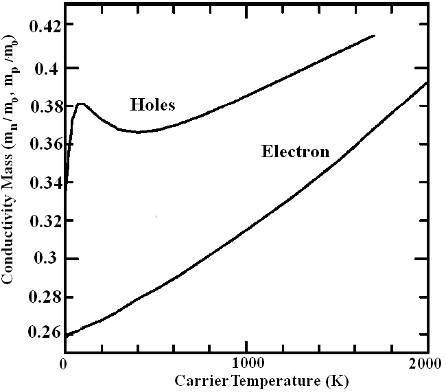
  The low-field value of the average electron mass, mno, is equal to the conductivity effective mass at the conduction band edge, and can be measured using the optically-detected cyclotron resonance (ODCR). The ODCR method is more accurate than the classical CR and has been recently used to measure the effective mass of several semiconductor compounds [118]. According to the optical measurements of Rife [119] the conductivity effective mass at 300K mno =0.275mo and mno =0.365mo as shown in figure 4(b). The ultrafast laser based pump-probe techniques have been used to measure the energy relaxation as well as the momentum relaxation times in Si. Using this technique, a time constant of 32±5 fs associated with momentum relaxation and an electron-phonon energy relaxation time of 260±30 fs have been extracted from the coherent-transient variations in (001) Si at 300K [120]. In order to verify our model, we used the MC simulation to calculate the average electron mass as a function of the average electron energy, and compared it with the measured ratio of (mno/mn), as shown in Figure 5. As shown in figure, the normalized value of the average inverse mass decreases as the electron energy increases. Then we calculated the energy relaxation time
  using the above phenomenological relation (above
  when electrons start to warm up). As shown in Figure 5, the discrepancy between the the energy relaxation time, according to MC and the calculated values according to our model lies within the measurement error (~10%) for a wide range of carrier temperatures (up to 2000K and may be extrapolated to higher values). Alternatively, our model can be used to calculate the energy dependence of the average electron mass
  from the energy dependence of the electron energy relaxation time
  The energy dependence of
  of several semiconductors (e.g., AlGaAs/GaAs, AlGaN/AIN/GaN) has been measured using the microwave-noise method [121]. This method is based on the measurement of the noise temperature, which is equal to the electron temperature Tn in the semiconductor, according to the following relation:
  | (35) |
 However, we have no experimental data yet about the energy relaxation time in Si (as a function of carrier temperature or energy) using this method. So, the proposed model which correlates
  to the already measurable
  should be very useful in this case.
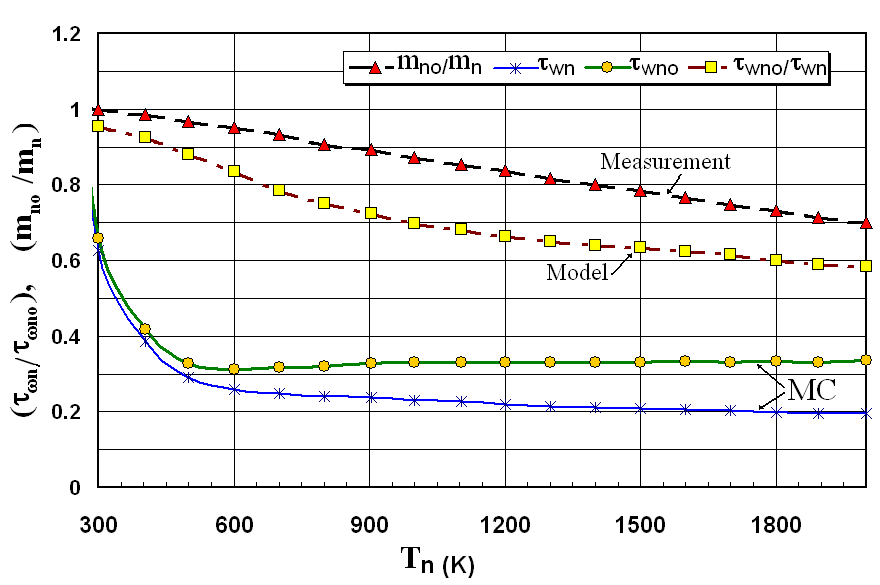 | Figure 5. Comparison between the normalized inverse mass (mno/mn), according to optical measurement [52] and our model. The model is calculated from the normalized energy relaxation time  according to MC data, by our phenomenological relation (25) according to MC data, by our phenomenological relation (25) |
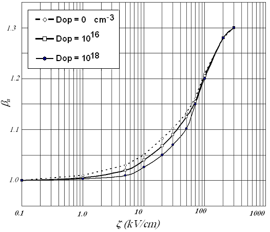 | Figure 6 (a). Heat flux beta factor in Si at 300K, calculated from MC simulation, with non-parabolicty factor 0.5V-1 |
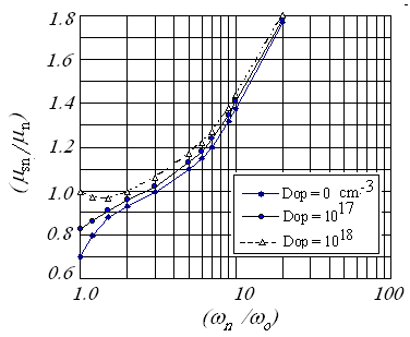 | Figure 6(b). Relative energy flow mobility in Si at 300K, calculated from MC simulation, with non-parabolicty factor 0.5V-1 |
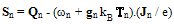
5.4. Advanced Heat Flux Model
- As we pointed out earlier, the heat flux term in the majority of previous HDM’s was either neglected or modelled by the Fourier relation (12-a). It has been shown that this model is not accurate for modelling the heat flux across semiconductor interfaces in general and p-n junctions in particular [122]-[124]. In order to increase the accuracy of the hydrodynamic model, we propose the following model, which is based on the third moment of the BTE in steady state:
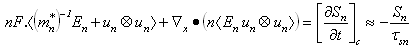 | (36.a) |
 is the energy flux relaxation time). The above conservation equation (of energy flux), may be further simplified by approximating the average terms, as follows [123]:
 | (36.b) |
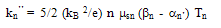
 ’ expresses the anisotropy of the distribution function and the correction factors
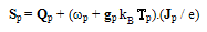
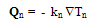
  expresses how much the distribution function is deviated from the Maxwellian distribution. These parameters can be estimated by MC simulation in the bulk of semiconductor. Then we can write the energy flux as the sum of a conduction part Qn and a convection part (where Jn is a multiplier):
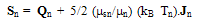 | (36.c) |
 and the electron heat flux Qn (
 ) is given by:
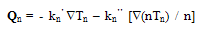 | (37.a) |
 | (37.b) |
 | (37.c) |
 and that
  is replaced with 5/2(kBTn). However, we just called the third moment equation in order to derive a more accurate formula of the heat flux term., which contains the effect of both the carrier temperature and the carrier density gradients.
 5.5. Modified Wiedman-Franz Relation
- If the anisotropy of the distribution function is negligible, we can substitute
 Then the heat flux term can be put in the following simple form:
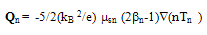 | (38.a) |
 as a function of electron energy. We calculated these parameters by MC simulation in the bulk of Si at 300Kwith non-parabolicity factor 0.5V-1. Alternatively, they may be evaluated, as functions of carrier energy, and doping level, by appropriate physical models. For instance, the energy flux mobility may be modelled in much the same way as the drift mobility as follows [124]:
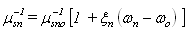 | (38.b) |
 is the energy flux mobility at low field and
 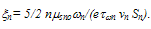 Also, the heat flux beta factor may be approximately expressed as follows in Si at 300K:
 | (38.c) |
 are constants. For Si at 300K with doping levels Dop ≤1019cm-3 and electron energy
  , we have:
  ,
,  .When the carrier-concentration gradient is negligible (with respect to the temperature gradient), the heat flux formula (35-a) can be further reduced to the conventional Fourier relation (12-a), with the following carrier-thermal conductivity:
  | (39.a) |
 | (39.b) |
 as compared to (5/2+r) in the conventional model (12-c). Figure 13 depicts the heat flux as obtained by the classic Fourrier relation and the new model. As shown in figure, the consideration of the carrier gradients in the new model broaden and smooth the heat fluc profile near junctions.
 5.6. Tunneling & Hot Carrier Injection Currents
- The tunnelling and hot carriers injection currents paly an important role in modern semiconductor devices in general and the ultra short MOSFET devices in particular. There are two tunnelling (through the barrier) mechanisms and four hot carrier injection (over the barrier) mechanisms which are commonly encountered in MOSFET devices, namely:● Field-assisted (Fowler-Nordheim or FN) tunnelling,● direct tunnelling (DT),● drain avalanche hot carrier injection (DAHCI), ● channel hot electron injection (CHEI),● substrate hot electron injection (SHI) and● secondary generated hot electron injection (SGHEI)These mechanisms are usually monitored by measuring the gate current, IG, and the substrate current, Isub. In the following subsections we describe briefly these parameters and how they are modeled within the framework of the hydrodynamic model.
5.6.1. Tunneling Currents
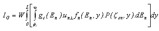
- The tunnelling currents are either direct or of field-assisted (Fowler-Nordheim) type. The direct tunnelling can take place at low gate voltages via thin oxides layers (less than 50Å) and has a weak dependence on the gate field. The FN tunnelling is a field-assisted mechanism which is strongly dependent on the gate field and dominates in modern MOS structures. The gate tunnelling current density is given by the following integration [125]:
 | (40) |
 is the electron group velocity perpendicular to the Si surface
  . The integration in the above equation starts from the semiconductor conduction band edge, as a reference. For trapezoidal barrier of upper height
  and lower hight (
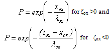
 ), where Vox is the potential voltage across the insulator gate, the tunnelling probability is usually expressed using the WKB approximation as follows:
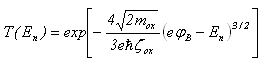 | (41.a) |
 , and
, and 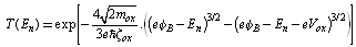 | (41.b) |
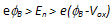
 . Here
  are the electric field and effective mass of electrons at the insulator (for SiO2, mox =0.42m0). In the case of the field-assisted Fowler-Nordheim mechanism, we consider the triangular part of the barrier, which is described by (38-a). Assuming the energy distribution function Maxwellian and the energy bands parabolic, we get the following field-dependent gate current density:
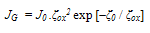 | (42) |
 are constants, related to the energy barrier height
  between the insulator and the injecting conductor as follows:
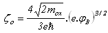 | (43.a) |
 | (43.b) |
 | (44.a) |
 | (44.b) |
 | (45.a) |
 | (45.b) |
 is the mean free path of electrons inside the gate oxide (for SiO2,
  ). In order to account for both tunnelling and thermoionic emission, the above equation should be modified as follows [127]:
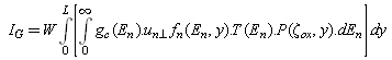 | (45.c) |
5.6.2. Hot Carrier Injection Currents
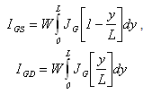
- The channel hot electron injection (CHEI) occurs when the gate voltage is high enough and VG ≈VD. Channel carriers which are accelerated by lateral fields and transported from the source to the drain may be driven towards the gate oxide before they reach the drain. The drain avalanche hot carrier injection (DAHCI) occurs when a high drain voltage is applied in non-saturation mode (VD>VG) which results in a high electric field near the drain, and hence accelerating channel carriers into the drain depletion region. The accelerated channel carriers collide with Si atoms valence electrons, creating electron-hole pairs by impact ionization. Some of the generated electron-hole pairs are again accelerated and may acquire sufficient energy to surmount the Si/SiO2 barrier. The hot carriers that surmount the gate oxide barrier can inject into the gate oxide where they may be trapped and gives rise to a shift in the MOSFET threshold voltage, surface mobility and dynamic conductance. The substrate hot electron injection (SHEI) occurs at high substrate bias, |VB| >> 0 and strong inversion, usually with both drain and source grounded. Under this condition, carriers of one type in the substrate are driven by the substrate field toward the Si-SiO2 interface. Carriers can be generated by external optical or thermal excitation. As carriers move toward the substrate-oxide interface, they gain further kinetic energy from the high field in surface depletion region. They eventually overcome the surface energy barrier and get injected into the gate oxide, where some of them are trapped. The secondary generated hot electron injection (SGHEI) occurs under conditions similar to DAHCI, when VD>VG, which lead to impact ionization of hot carriers. However, SGHEI involves secondary carriers that are created by an earlier incident of impact ionization and driven under the influence of the substrate bias. This bias produces a field that drives hot carriers toward the surface region, where they gain more energy to overcome the gate oxide barrier [124]. The so-called “channel-initiated secondary electron (CHISEL) is a variant of the SGHEI, which relies on ionization feedback and is activated by a negative substrate bias VB<0. CHISEL is used as a reliable programming technology in recent low-voltage Flash EEPROM devices, with floating gate lengths down to 0.2
 [131]. Figure 18 illustrates the different hot injection and tunnelling mechanisms in MOSFET devices.The injection of hot-electrons into the gate-oxide has been usually modelled by the lucky-electron model [83]. According to Hu et al., the probability of a channel electron reaching the gate terminal as a combination of the probabilities of the following events:● the electron gains sufficient energy in the lateral electric field to overcome the interfacial● potential barrier and retains this energy after a collision directs its momentum towards the interface,● the electron reaches the interface without suffering any more collisions, and● the electron is not scattered back into the semiconductor in the image-force potential well present close the interfaceThe lucky-electron model, despite of its drastic assumptions, remains the most useful approach to estimate the injection currents with reasonable agreement with experimental results. On the basis of the lucky-electron model, it can be shown that the fraction of the channel carrier supply which is injected into the gate oxide is given by [129] :
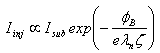 | (46.a) |
 is the interfacial potential barrier,
  is the electron mean free path and
  is the effective lateral electric field. It can be shown that the effective barrier potential
  is given by:
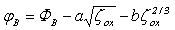 | (46.b) |
 a and b are constants, expressing the main barrier height and lowering effects due to image force and quantum tunnelling. For Si/SiO2 interface,
  , a = and b = 2.59x10⁻⁴ (Vcm)½. As the substrate current is generated due to impact ionization in the lateral electric field close to the drain, it is linearly proportional to the drain current. On the basis of the lucky-electron concept, it can be shown that the substrate currents is given by :
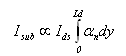 | (47) |
 is the electron impact ionization coefficient in the velocity saturated part of the channel. So, the substrate current can be given by:
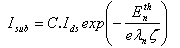 | (48) |
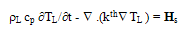
6. Lattice Heat Conservation Equation
- Some recent studies demonstrated the important role of lattice heat and thermal activation of the low voltage impact ionization in deep-submicrometer MOSFETs [132]. In addition, the recent studies of silicon on insulator (SOI) devices by the classical HDM, showed certain anomalies due to lack of a heat evacuation mechanism at the insulator interface [133]. Some authors suggested to cure this problem by considering a tensorial temperature and modifying the closure condition for energy flux term [134]. Othors authors suggested coupling the lattice heat equation to the set of HD equations [135]. The classical heat diffusion equation, which resolves the temporal and spatial distribution of lattice temperature along the semiconductor, reads:
 | (49.a) |
 is the lattice density, cp is the lattice specific heat and their product is equal to the heat capacitance (
 ) of the semiconductor material. Also kth is the thermal conductivity of the semiconductor and the heat source term Hs is given by [136]:
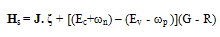 | (49.b) |
 is the absolute average electron energy and
  is the absolute average hole energy in the crystal lattice. In Si at 300K,
  gm/cm3 and cp =7.03x104 cm2/Ks2 and their temperature dependence is negligible [137]. We dully note that the carrier thermal conductivity is a small fraction of the Si material thermal conductivity kth because heat conduction in semiconductors is dominated by phonon transport. It should be also noted that for TL > 100K, the thermal conductivity in Si is practically independent of doping concentration [ 138]. The temperature dependence of kth in the bulk of crystalline Si may be modelled according to Glassbenner and Slack [139] as follows:
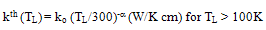 | (49.c) |
 and ko ≈ 1.45 for Si. However, in thin semiconductor layers the thermal conductivity is reduced due to the phonon scattering process at layer boundaries (the size effect), as described in [140]. An analytical expression describing the thermal conductivity as a function of distance, into thin Si layers can be found in [141]. A more rigorous approach to solve the problem of heat evacuation in SOI devices, consists in solving the BTE for phonons. In fact it is well known that the LO phonons have small group velocities (~105 cm/s) and anharmonically decay into faster acoustic phonons which in turn transport the energy out off the semiconductor device. So, the phonon BTE may be simplified by assuming a two-fluid phonon transport model involving a stationary optical reservoir mode and a propagating acoustic mode. The latter approach may consider not only the heat evacuation by optical phonons, but also their anharmonic decay to ‘fast propagating’ acoustic phonons. As a compromise between the above mentioned approaches, the a lattice heat continuity equation may be added to the set of HDE’s with phonon energy relaxation term. The transformed phonon BTE in the relaxation time approximation reads [142]
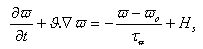 | (50.a) |
 is the phonon energy per unit volume, υ the phonon velocity and
  is the phonon energy relaxation time and Hs is the volumetric heat generation rate absorbed from hot electrons, which can be extracted from the solution of the HDE’s. According to the kinetic theory, the phonon energy relaxation time is related to the phonon velocity vph and mean-free path
  by the following relation [143]:
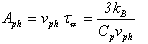 | (50.b) |
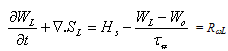 | (50.c) |
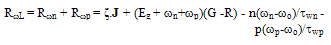 | (51.a) |
 is equal to the RHS of the energy conservation equation (10-c) for electrons and
  for holes. When the net generation-recombination rate is negligible,
  represents the local energy transfer rate from crystal lattice to the electron and hole gaz subsystems. Therefore we can write the following correlation function between the charge carriers relaxation times and phonons relaxation time:
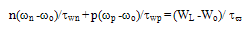 | (51.b) |
7. Quantum Corrections
- The so-called quantum hydrodynamic model (QHDM) can be derived by a variety of methods [144-152], such as the first few moments of the WBTE or using the Madelung transform [147] or the principle of minimum entropy [148]. The formulation of the QHDM usually retains the lowest order
 term in the series expansion of a complicated quantum operator acting on the Wigner distribution function and the system potential energy. From the mathematical point of view, the most significant difference between the semiclassical HDM and the QHDM is the quantum potential term, Vq, which appears in the average energy expression [150]:
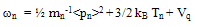 | (52.a) |
 is the average momentum of electrons and Vq is given by:
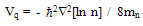 | (52.b) |
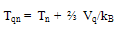 | (52.c) |
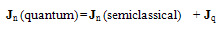 | (53.a) |
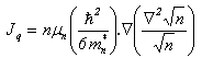 | (53.b) |
8. Quasi-Ballistic Transport Considerations
- It has been shown that the operation of sub 0.1 micron MOSFET transistors is quasi-ballistic, in a small portion of the channel [153-158]. Some authors shows that quasi-ballistic transport in nano-transistors takes place near the source region and others showed that quasi-ballistic transport and back scattering take also place near drain region as well [157]. In all cases, one should be aware that even when the transport is full ballistic, the contact resistance of the device is still there limiting the transport process. However, the quasi-ballistic transport can be also considered within the framework of the semiclassical theory [156]. In fact, it has been shown that semiclassical transport models along the MOSFET channel may remain reliable down to 10nm [157]. In addition, it has been shown in the latter article, that the semiclassical model is more reliable than the quantum simulation, even when the ratio of coherent transport along the MOSFET channel is not negligeable (down to 10nm). Figure 7 depicts the electron velocity distribution along a 50nm n-i-n structure, in the ballistic mode and using different transport approaches.
9. Sample of Simulation Results
- Figure 1 depicts the electron temperature Tn, according to Monte Carlo simulation, the classic HDM and according to our definition. As shown in figure, the electronic temperature is reasonably estimated using our model when taking gn≈1, for electric field up to 200 kV/cm. For the matter of demonstration of the proposed HDM and comparison with other DDM-based simulation, we simulated the carrier transport across a reverse-biased silicon p-i-n diode. The simulated diode is 100m long and has a p+ side with Gaussian distribution and peak doping of 1019cm-3., as shown in Figure 8. The diode base n--layer is homogenously doped with 1014cm-3, and the metallurgical junction is almost at 11
 apart from the p+ contact. Figures 9 and 10 depict the two-dimensional distributions of electron and hole density and temperatures inside the p-i-n diode at 75V reverse bias. Figures 11 and 12 depict the one-dimensional distributions of electron and hole density and temperature along the p-i-n diode at 500V reverse bias. Also figures 13 and 14 depict the one-dimensional distributions of electron and hole energy flux and heat flux along the p-i-n diode at 500V reverse bias. In addition. Figure 15 shows the I-V characteristics of the simulated diode near breakdown. We discussed in [159] the effect of the hydrodynamic simulation on the distribution of charge carriers and showed that discrepancy from the DDM-based results is due to the carrier thermal back diffusion. In order to show the important role of the energy relaxation time model in the HD simulation, we traced the electron distribution across the p+-n junction at various values of the
  Figure 16 depicts the electron density distribution along a reverse biased p-i-n diode at three values of the energy relaxation time. Note that the electron distribution, which is obtained using the HDM with lower
  tends to the DDM classical distribution. This means that for shorter energy relaxation times, the electrons are more efficient in dissipating their energy. For the limiting case when
  tends to zero, the electrons will tend to dissipate their gained energy at once and their average energy is equal the lattice energy
  This is exactly the case of the DD simulation, where we consider the electron temperature equal to the lattice temperature (Tn=TL) at all fields.
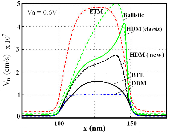 | Figure 7. Effect of quasi-ballistic transport on the electron velocity across an n-i-n diode, according to several models [118] |
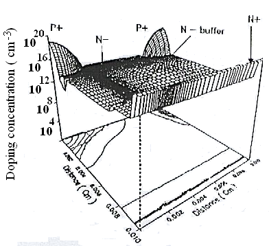 | Figure 8. (a) Two-dimensional doping profile of the simulated p-i-n diode |
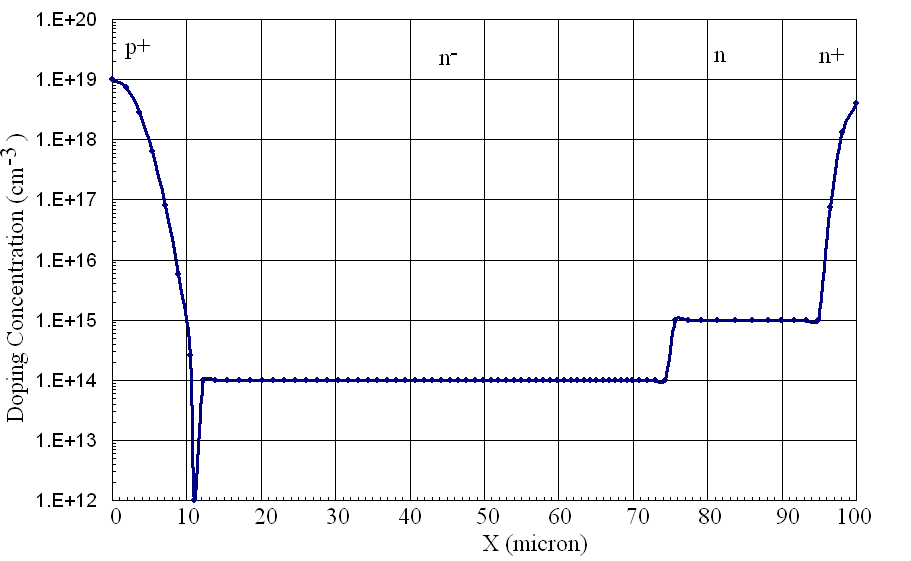 | Figure 8. (b) Lateral doping profile along the x-axis of the p-i-n diode |
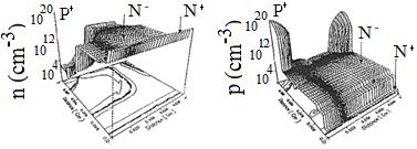 | Figure 9. (a) Electron and (b) hole density distribution in the p-i-n diode (at –75V bias) |
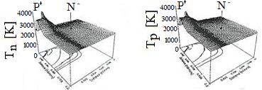 | Figure 10. (a) Electron and (b) hole temperature distribution in the p-i-n diode (at -75V bias, 300K) |
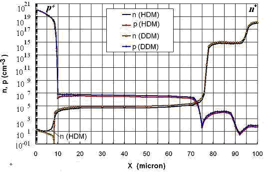 | Figure 11. Electron density distribution along the p-i-n diode (at 500V reverse bias, 300K), on the basis of DDM and HDM |
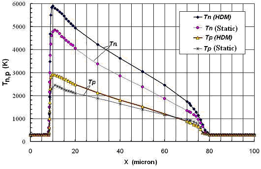 | Figure 12. Electron and hole temperature distribution along a reverse biased p-i-n diode (at –500V), as calculated from the DDM electric field distribution (static) and by HD simulation |
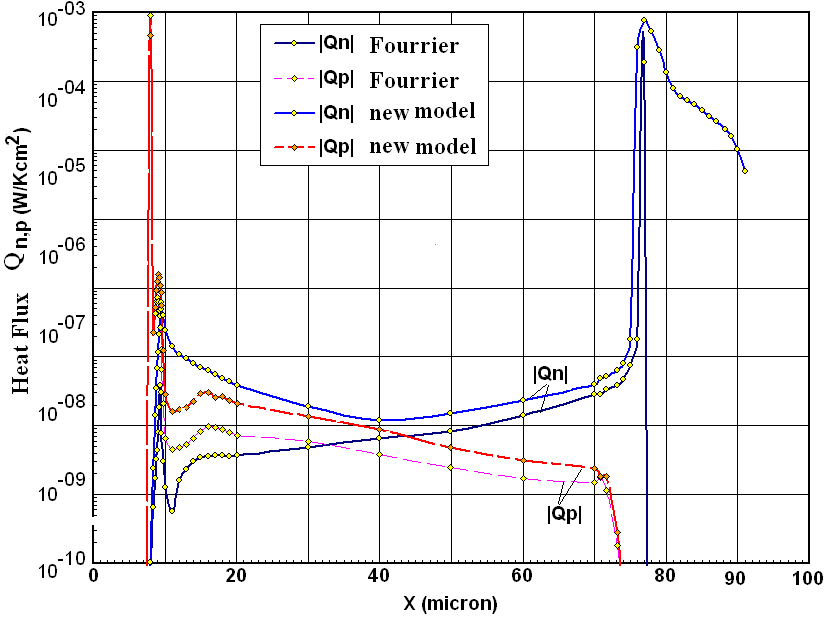 | Figure 13. Electron heat flux distribution along the p-i-n diode at 500V reverse bias, 300K |
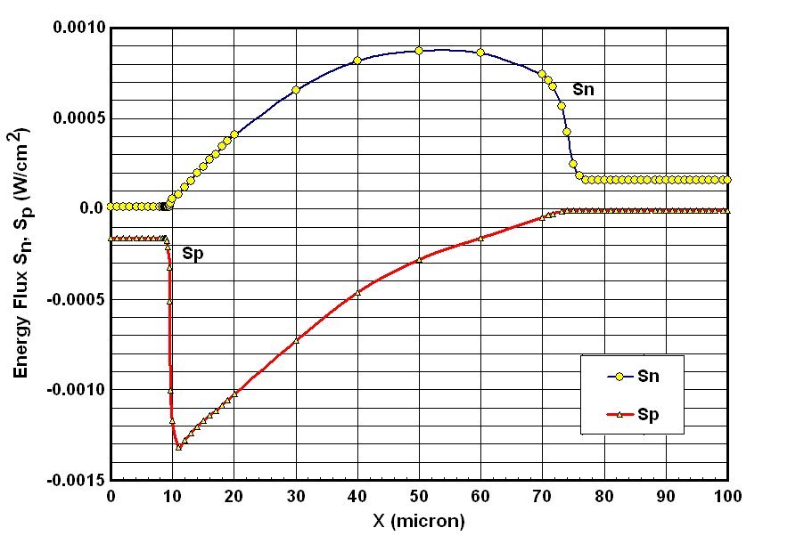 | Figure 14. Electron energy flux distribution along the p-i-n diode at 500V reverse bias, 300K |
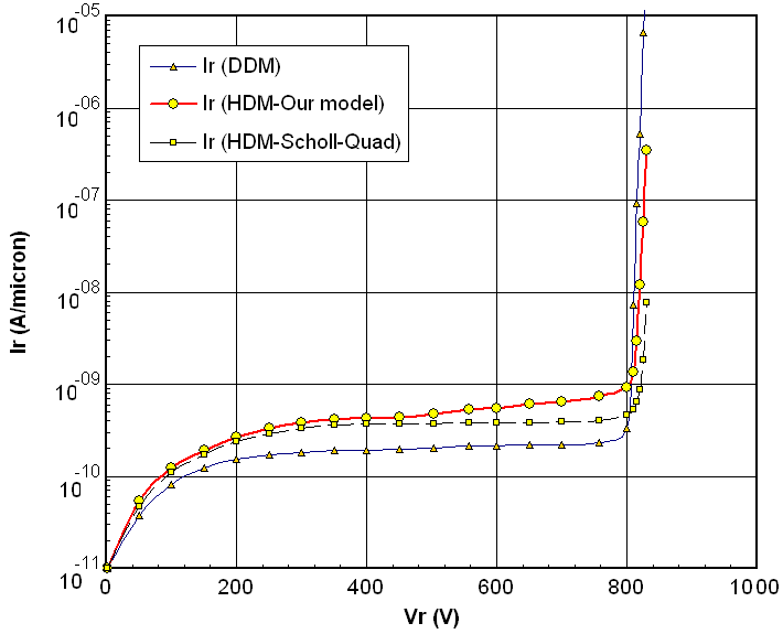 | Figure 15. The I-V characteristics of the simulated the p-i-n diode near avalanche breakdown, as obtained by 2-dimmensional DD and HD simulation at 300K. The surface of the p-i-n diode is properly passivated and protected by field plates, so that the breakdown occurs at the junction curvature inside the p-i-n diode |
 | Figure 16. Electron density distribution along a reverse biased p-n junction, with different values of energy relaxation time |
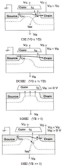 | Figure 17. Illustartion of different hot carrier injection mechanisms in MOSFET Devices |
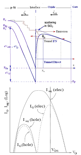 | Figure 18. Illustration of hot carrier injection currents in MOSFET Devices |
 | (54) |
 and hence
  and this case means a virtual semiconductor whose collisions are so efficient that electrons relax to their equilibrium energy in almost no time.
 | (54) |
 will be almost equal to the lattice energy
  This result has been already reported for majority carriers in MOSFET devices [97], but has er been reported for minority carriers in bipolar devices, as far as the author knowledge.
10. Conclusions
- In conjunction with sophisticated Monte Carlo methods that incorporate both realistic band structure and carrier scattering processes, the HDM is a basic tool to understand hot carrier behaviour in ever smaller and ultra fast semiconductor devices. We presented in this article a complete hydrodynamic model based on the first three moments of the semiclassical BTE for electrons, holes and phonons, with a few number of parameters. The model includes the band structure non-parabolicity effects and advanced energy-dependent models of the carrier mobility, impact ionization rate and heat flux. As the accurate estimation of the carrier temperature in semiconductor devices, influences the estimation of so many important parameters, such as the breakdown voltage and leakage currents, we proposed a simple definition of the carrier temperature, which takes the band structure into account. The definition results in temperatures which are closer to the simulation results than those obtained by the classical hydrodynamic models. We also proposed a phenomenological correlation between the electron average mass and energy relaxation time which cuts down the number of parameters of the HDM. In conclusion, our proposed system of HDE’s has a few energy-dependent parameters
 and they are all correlated to the energy relaxation time
  The later parameter can be obtained from the MC simulation [161] or by measurement. The proposed model has been applied to investigate the carrier transport in certain semiconductor devices and led to adequate results. From our simulation, we conclude that the undeliberated choice of the energy relaxation time value in the HD simulation leads to drastic results and may be to the failure of the HDM in certain cases, as reported in [47]. For instance, we show, by simulation, that reducing the energy relaxation time to unreasonable short values will mask the thermal diffusion mechanism and gives erroneous results, in both MOSFET and bipolar devices.
 APPENDIX: Moments of the BTE
- Consider the distribution function f(x,k,t), which obeys the BTE. Consider A(k) a microscopic quantity, which is a function of the wave vector k. Now, let’s multiply the BTE by A(k) and integrate the two sides of the equation over the entire k-space:
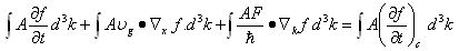 | (55) |
 , which we note by
  is given by:
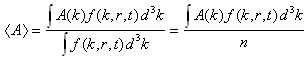 | (56) |
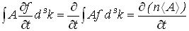 | (57-a) |
 | (57-n) |
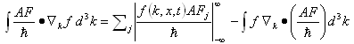 | (57-d) |
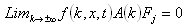 . This means that all the moments of the BTE are finite. On the other hand, the second term of (I-2c) may be written as follows:
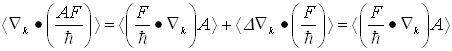 | (57) |
 , which is true if F is independent of k or when F is normal to k. Fortunately, this is the case for electric field force (
 ) and Lorentz’s force (
 ). Now, by regrouping all (55) components we get:
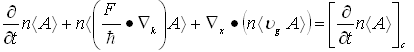 | (58) |
 and
and  we obtain the 3 moment equations of the BTE. Table 1 summarizes the results.
|