-
Paper Information
- Next Paper
- Previous Paper
- Paper Submission
-
Journal Information
- About This Journal
- Editorial Board
- Current Issue
- Archive
- Author Guidelines
- Contact Us
Microelectronics and Solid State Electronics
p-ISSN: 2324-643X e-ISSN: 2324-6456
2012; 1(5): 111-117
doi: 10.5923/j.msse.20120105.02
A New Spice Macromodel of 4H-SiC Vertical Double Implanted MOSFET (DIMOS)
 Abstract
 Reference
 Full-Text PDF
 Full-Text HTML
Messaadi Lotfi, Dibi Zohir, Smail Toufik
Department of Electronics, University of Batna, Advanced Electronic Laboratory (LEA),Av. El HadiBoukhloufBatna, 05000, Algeria
Correspondence to: Messaadi Lotfi, Department of Electronics, University of Batna, Advanced Electronic Laboratory (LEA),Av. El HadiBoukhloufBatna, 05000, Algeria.
| Email: |  |
Copyright © 2012 Scientific & Academic Publishing. All Rights Reserved.
The4H-SiCvertical double Implanted MOSFET (DIMOS) offers advantages over conventional silicon devices, enabling high system efficiency and/or reduced system size, weight and cost through its higher frequency operation. Compared to the best silicon IGBTs, the SiC device will improve system efficiency up to 2% and operate at 2-5 times the switching frequencies.In this paper we present an equivalent circuit Spice of 4H-SiC DIMOSFET for a wide temperature range. Simulation for DC characteristics (I-V) of the SiC MOSFET with the exact device geometry is carried out using the commercial device simulator Spice. All Spice parameters are extracted from the measurements, and a SPICE model for the DIMOS transistor has been developed and implemented in the circuit simulator Orcad PSpice 10.5. The temperature dependent behaviour was simulated and analysed. A good agreement between the Spice simulation and analytical model evaluation for SiC DIMOS is demonstrated. Model parameters can be adjusted to obtain an optimum device to be used in power system applications.
Keywords: Power Device, 4H-SiC DIMOSFET, Macromodel, Analytical Model, Spice, Temperature Variation Effect
Cite this paper: Messaadi Lotfi, Dibi Zohir, Smail Toufik, "A New Spice Macromodel of 4H-SiC Vertical Double Implanted MOSFET (DIMOS)", Microelectronics and Solid State Electronics, Vol. 1 No. 5, 2012, pp. 111-117. doi: 10.5923/j.msse.20120105.02.
Article Outline
1. Introduction
- With increasing global emphasis on energy efficiency, improved power devices are critical to the development of the next generation of power systems. Increasing the efficiency of power conversion systems produces multiple benefits. Increasing the efficiency of a system has the obvious benefit of increasing the power output of the system[1], and it also has the benefit of reducing the amount of waste heat being generated, leading directly to a reduction in the size, weight and complexity of the cooling system. Further decreases in size and weight can be achieved by operating the system at a higher frequency, thereby reducing the number and mass of passive components.SiC, a wide bandgap semiconductor material has an electric-field breakdown capability that is ten times that of silicon and also has excellent thermal conductivity. SiC is also a robust material since it is both physically hard and maintains its properties at extremely high temperatures [2].Although there are no commercially available power MOSFETs in SiC material, Cree has demonstrated various switching devices in SiC A group from Purdue University proposed a DIMOS in 6H-SiC with a breakdown voltage of 760V[3] Presently, most of the research effort in SiC is on the design and fabrication of power MOSFETs. However, theoretical models of these prototypes have to be developed to study the behaviour of these devices and fine-tune their characteristics. Since SiC MOSFETs are still in their infancy, there is a good opportunity now to study and model these devices so that the model can be verified using actual SiC MOSFET test devices. A good reliable device model is essential for the evaluation of the device behaviour and its characteristics[3]. A precise model can predict the device behaviour more accurately and thus, the design requirements can be implemented with tight tolerances. This paper provides a brief overview of the state-of-the-art research in the area of silicon carbide device modelling. A thorough and detailed analysis of a SiC power MOSFET, modelling, simulation, testing, and characterization of a test device and the extraction of parameters for a SPICE model are presented. SiC offers significant advantages for power electronics applications such as lamp ballasts, motor controls, medical electronics, automotive electronics, high- density high-frequency power supplies and smart-power application-specific integrated circuits. Hence, silicon carbide-based MOSFET can be used in high power application and hence MOSFETs require a high breakdown voltage. The one-step field plate termination can enhance the breakdown voltage to 910 V, embedded mesa termination can increase it to 1350 V and the embedded mesa with step field plating can give a breakdown voltage of 1100 V. However, 4H-SiC DIMOSFETs in practice have attained a maximum blocking voltage of 760 V. The specific on-resistance of the drift region of the MOSFET can be significantly reduced by enhancing the inversion channel mobility using phytogenic re-oxidation annealing thereby reducing the power dissipation. The present work aims at estimating theoretically the breakdown voltages, power dissipation and specific on-resistance at various doping levels by varying the drain voltage[4].The long term goal of this program is to develop SiC power switches with a 2.5kV blocking voltage and a 50 A current rating for insertion into motor control modules operating at temperatures as high as 200℃.
2. Modelling of Vertical DIMOS Device
2.1. Model
- An analytical model for a DIMOS field effect transistor is developed using SiC material[5]. The model is developed based on the methodology for a vertical double diffusion MOS model. The proposed DIMOS model incorporates the effect of SiC device behaviour. Figure 1 shows the details of the device structure identifying the different regions of operation. The model is developed from regional analyses of carrier transport in the channel and the drift regions. The active channel exists below the oxide layer and within the p-bodies. The current/voltage characteristic in the triode region is given by Eq. 1
 | (1) |
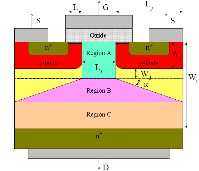 | Figure 1. DIMOS structure for modeling. Labels describe the different regions and dimensions of the vertical structure |
 | (2) |
 | (3) |
 | (4) |
 | (5) |
 | (6) |
 | (7) |
 | (8) |
 | (9) |
 | (10) |
 | (11) |
3. Device Structure
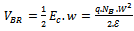
- A vertical double implanted MOSFET (DIMOS) in 4H-SiC is considered for verification of the analytical model developed earlier. The cross-sectional view of the proposed DIMOS structure is shown in Figure 2. The proposed device structure and the device dimensions are selected in such a way that a practical device can be built on the basis of currently available SiC technology. Since the diffusion process in SiC is negligible, ion implantation is the only way to form the p-bodies and the n+ region for the vertical structure. Double diffusion is not suitable for SiC device fabrication. Double implantation technology consists of the deep range acceptor followed by the shallow range donor implantation to build the necessary MOSFET structure. The thickness and the doping level of the drift region largely determine the breakdown voltage of the device. The larger the thickness of the drift region is, the bigger the blocking voltage is. However, the current SiC technology has a limitation of the achievable epilayer thickness. In this design, a 3kV MOSFET is considered, and the corresponding epilayer thickness is taken as 25 μm. Based upon the recent SiC fabrication technology, this epilayer thickness is certainly achievable. Recently, Agarwal and alain[7] achieved epilayer thickness of about 115 μm, which allows the blocking voltage to be around 10 kV. The n- drift region is usually doped lightly (4x1015cm-3 for this device) to obtain the desired blocking voltage of the MOSFET operation. The n+ regions are doped with (1.5x1020cm-3) Nitrogen, and the p-bodies are formed with (4x1017cm-3) Aluminum implantations. The channel length and the width are taken as 1μm and 400 μm, respectively. The oxide thickness is 500 Å, and the p-bodies are separated by 20 μm.Table 1 shows values of doping concentration,electron mobility, drift layer thikness and specific on-resistance as a function of breaksown voltage for ideal 4H-SiC and Si power MOSFETs at room temperature condition[8-10].
|
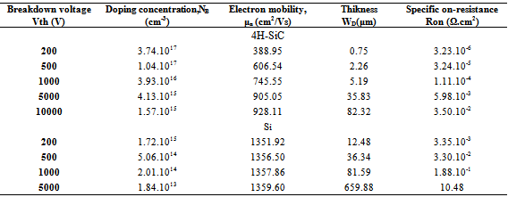
 | Figure 2. Schematic cross section of vertical DIMOS structure |
 | Figure 3. Equivalent SPICE model of 4H-SiC MOSFET transistor |
4. Macromodel Structure
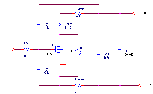
- A simple behavioural SPICE model for the SiC DIMOSFET is proposed based on the understanding of the power MOSFET device terminal behaviour (Figure 3). The aim of the model development is to reuse the available built-in FET models of the regular lateral MOS devices of the commercial SPICE simulator[11]. The advantage of the model is the limited number of required parameters, which can readily be extracted from simple terminal measurements or from standard datasheets, using the algorithmic and empirical approach as described below. Once the parameters are placed, the model can be used to simulate either p-channel or n-channel SiC power MOSFET devices over a wide range of currents and voltages.The model especially considers silicon carbide material and process related parameters that affect the device performance. The model can be described as a sub-circuit within the same SPICE code and can be run in any commercial SPICE simulator. Since DIMOS is a power device, its channel length, width, and other device dimensions are big enough to neglect the second order effects in the model equations, and the simulation can be carried out as SPICE level 1 or level 2[12-13]. Due to larger gate area, power MOSFETs show large gate capacitance. The major three capacitances considered in the model are: gate-source capacitance (CGS), gate-drain capacitance (CGD), and drain-source capacitance (CDS). These capacitances show considerable effects on switching characteristics or dynamic behavior of the device. Power 4H- SiC MOSFETs model represented in Figure 4 can block the voltage in reverse bias condition. This blocking capability is usually represented by the reverse bias body diode, which is formed between the p-bodies and n-drift region of the vertical structure. The effect of channel resistance variation with gate bias is represented by the dependent current source IRCH. The current from the dependent current source increases with an increase in the gate voltage. The proportionality constant of the dependent current is determined from the empirical fit of the measured data[14-16].
 | Figure 4. The model of 4H-SiC MOSFET inserted in Spice library |
5. Simulation Results
- The figures below show typical DC simulation results. The model is able to reproduce thestrong quasisaturation effect in the devices and still retain a good fit for the currents nearthreshold.
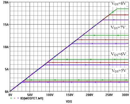
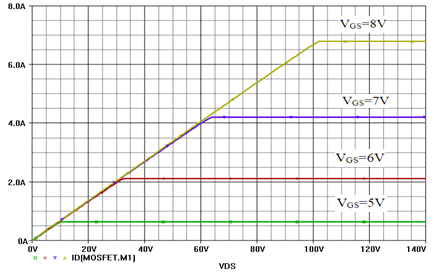 | Figure 5. Forward characteristic simulation of 4H-SiC MOSFET |
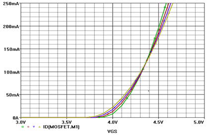
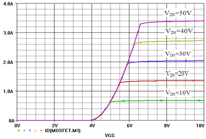 | Figure 6. Characterization of ID versus VGS by stepping VDS |
 | Figure 7. Transfer characteristics of 4H-SiC MOSFET at different temperature: T=50°C,100°C,150°C and 200°C (Green to Yellow) |
 | Figure 8. Forward characteristic simulation of 4H-SiC MOSFET at T=50°C, 100°C and 150°C (Green to Blue) |
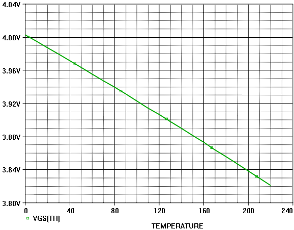 | Figure 9. Threshold voltage simulation of 4H-SiC MOSFET (ID=50mA and VDS=VGS) |
6. Conclusions
- In this paper, a vertical double implantedMOSFET in 4H-SiC material system for power electronic applications has been tested and modelled. The static characteristics, such as the forward and transfer curves and threshold voltage have been extracted and simulated under different temperatures, the macromodel of 4H-SiC DIMOSFET has been developed and inserted in the SPICE library. A device structure is also proposed to verify the model in 4H-SiC material. Temperature effect in DIMOS is observed. The temperature effects imposed on the drift region doping help to achieve a device structure for the desired current level and breakdown voltage. All SPICE parameters are extracted from the measured data. The simulation results matched very well with the measurements. The advantages of SiC power devices can be further demonstrated by somecircuit simulation, for example, an unclamped inductance circuit.
ACKNOWLEDGMENTS
- The author would like to thank Mr. Lotfi khadraoui for his great help.