-
Paper Information
- Next Paper
- Paper Submission
-
Journal Information
- About This Journal
- Editorial Board
- Current Issue
- Archive
- Author Guidelines
- Contact Us
Microelectronics and Solid State Electronics
p-ISSN: 2324-643X e-ISSN: 2324-6456
2012; 1(5): 102-110
doi: 10.5923/j.msse.20120105.01
Synthesis of Asynchronous Controllers on FPGA from Generalized Multi-Burst Graph Specification
 Abstract
 Reference
 Full-Text PDF
 Full-Text HTML
Duarte L. Oliveira1, Luiz S. Ferreira1, Leonardo Romano2
1Divisão de Engenharia Eletrônica do Instituto Tecnológico de Aeronáutica – ITA – São José dos Campos – SP, Brazil
2Departamento de Engenharia Elétrica do Centro Universitário da FEI – São Bernardo dos Campos – SP, Brazil
Correspondence to: Duarte L. Oliveira, Divisão de Engenharia Eletrônica do Instituto Tecnológico de Aeronáutica – ITA – São José dos Campos – SP, Brazil.
| Email: |  |
Copyright © 2012 Scientific & Academic Publishing. All Rights Reserved.
On promising area application of asynchronous is in Heterogeneous Systems (synchronous and asynchronous modules mixed). Asynchronous controllers are quite used in heterogeneous systems. The specification of theses controllers requires two types of signals: level sensitive signals that are used as conditionals and transition sensitive signals. Another requirement is to describe concurrency between inputs/outputs. The Multi-Burst Graph (MBG) specification allows to describing these controllers in a compact form and it is familiar to designers of digital circuits. This paper proposes a generalization in the MBG specification to increase the ability to describe the interaction between inputs/ outputs, i.e. increase the concurrency between them. This paper also proposes a method that starts from Generalized MBG specification and implements its hazard-free controllers on FPGAs. These devices have been mainly used for design of synchronous controllers. However, it is difficult to design asynchronous controllers on FPGAs, because the circuit may suffer from hazard problems. The method proposed implements this class of asynchronous controllers on FPGAs which are based on Look-Up Table (LUT) architectures. By doing this, the asynchronous circuits besides their intrinsic advantages over synchronous ones may also take advantage of integration, lower costs and short-time design associated with FPGA designs.
Keywords: Asynchronous Logic, Finite State Machine, FPGA, Hazard, Multi-Burst Graph, Synthesis, XBM Specification
Cite this paper: Duarte L. Oliveira, Luiz S. Ferreira, Leonardo Romano, "Synthesis of Asynchronous Controllers on FPGA from Generalized Multi-Burst Graph Specification", Microelectronics and Solid State Electronics, Vol. 1 No. 5, 2012, pp. 102-110. doi: 10.5923/j.msse.20120105.01.
Article Outline
1. Introduction
- There has been a growing interest in asynchronous circuits in recent years due to the increase in performance and complexity of digital systems[1]. Asynchronous circuits present several potential advantages over their synchronous counterparts: dissipate less power, do not present problems of clock skew and clock distributed network, and are more robust in respect to temperature variations andelectromag- netic interactions[2]. However it is not easy to design asynchronous circuits free of hazards and critical races[2].Two promising styles of asynchronous systems design are: micropipeline[3] and decomposition (controllers+data-paths) [4]. For a set of applications, as intensive control-flow design, the decomposition style is the most appropriate. The main reason is the non-pipelined nature of the applications. For this decomposition style different techniques were proposed to the synthesis of data-paths and controllers[5]. An important class of asynchronous controllers is one that obeys the delay model, Bounded Gated and Wire Delay (BGWD) [2],[6]. This model is realistic, it allows implementing these circuits with basic gates.
1.1. Specifications for Asynchronous Controllers
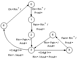
- Two important specifications for BGWD asynchronous controllers are: Signal Transition Graph (STG) and Extended Burst-Mode (XBM).STG: proposed by Chu in[7] is a Petri-net description (see Figure 1). The strength of STG is to describe concurrence between inputs and outputs (I/O concurrence) that occur in asynchronous systems. It naturally describes timing diagram that are quite used in the interfaces design. However, there are several descriptions in STG that aren’t implemented. The description becomes very confusing when it has to manipulate a larger number of signals. Furthermore, this type of description may explode in size and also the STG is not so familiar to designers of the synchronous world[8],[9].XBM: proposed by Yun and Dill in[10] is an extension of burst-mode (BM) specification proposed by Davis in[11] and formalized by Nowick in[12] (see Figure 2). It is suitable for to describe heterogeneous (synchronous / asynchronous) systems behavior, in the case asynchronous finite state machines in Mealy type. The XBM specification solves the problems related to the STG description but the XBM allows describing a limited I/O concurrency[1]. The XBM is the natural description of finite state machines1. These machines interact with the environment in generalized fundamental mode (GFM). In this mode, a new set of input signals will be activated only if the controller is in a stable state. The XBM specification added two signal types to the BM specification: directed don’t-care and conditionals. The latter are level sensitive signals (LSS), i.e., they are active during their “0”or ‘1” phase as opposed to all others that are transition sensitive signals (TSS), i.e., they are active during the “0→1 or 1→0” transition. LSS signals may present non-monotonic behaviour. A signal is either LSS or TSS (it may NOT change from one type to the other). Very good results were presented for XBM controllers like SCSI[13], differential equation solver[14] and instruction decoder[15]. Figure 2 shows the input signal Cntgt1 that is LSS and the input signals Ok, Fain, Rin are TSS.
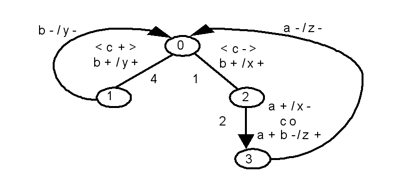
 | Figure 1. STG specification in[31] |
 | Figure 2. XBM specification: Scsi-init-send |
 | Figure 3. F_XBM specification: HP-Sbuf-Send-Pkt2 |
 | Figure 4. MBG specification |
1.2. FPGA Implementation of BGWD Controllers
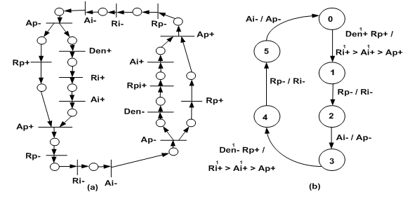
- FPGAs are popular components for prototyping and production of digital circuits due to their low cost and short-design time. Their focus has been on synchronous digital circuits. There have been some recent efforts to prototype asynchronous circuits on both commercial[23],[24] and academic FPGAs[25]. There are two reasons as to why off-the-shelf FPGAs are not fit to BGWD controllers[23],[26] and[27]:a. Mapping Process of hazard-free Booleans functions to logic blocks (macro-cells) may introduce logic hazards. The mapping free of logic hazard, should decomposed gates with fan-in related with LUTs[28]. Each gate is associated a LUT. b. Internal Routing Process among logic blocks may introduce significant delays that may result in essential hazard. This type of hazard can be solved by delay elements insertion or if the specification satisfied the requirement of essential signal[29]. This paper proposed a generalization of MBGspecifica- tion, through of extension of SEQ operator. The extension of the SEQ gives a better interaction with the environment in the I/O-Mode, i.e. increases the ability of to describe the I/O concurrency. We also proposed a method that starts from generalized multi-burst graph (GMBG) specification and synthesize asynchronous controllers. They are implemented in the feedback RS standard architecture (see Fig. 5) and interact with the environment in the GFM. This architecture is more robust to essential hazard, and the GFM enables the mapping free of logic hazard. The feedback in the RS architecture allows a covering hazard-free logic in the state transitions labelled with signals LSS and that operate with any machine cycle (for example: Input burst→ output burst // state variable)2. For implement on FPGAs the our GMBG controllers use a more robust logic minimization, where the controllers satisfy the delay model that is unbounded gate delay and bounded wire delay.
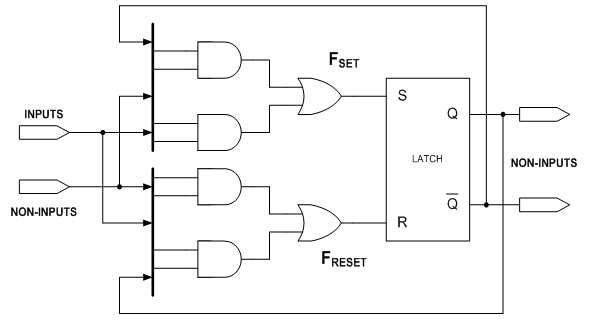 | Figure 5. Architecture: feedback RS standard |
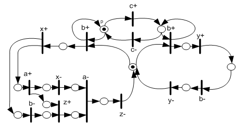
2. MBG Specification
- The Multi-Burst-Graph (MBG) specification belongs to a class of specifications that allow multiple-input change. The MBG is an extension of the XBM. As in the XBM, MBG is represented as a state graph where each node represents a state and each arc represents a transition. Each transition in the MBG can be activated by: 1) an input burst; or 2) a burst expression. The MBG introduced three operators: input burst (OR), transition concurrence (CO) and transition sequence (SEQ). The burst expressions are based on these operators, so it increases the possibilities to describe I/O concurrency. During the multi-burst transition is assumed that each output signal changes its value just once. If this assumption is not respected a functional hazard may occurs. As in the XBM, in order to guarantee the implementation of an MBG specification, it must obey restrictions in[20],[21].Figure 6 shows a MBG specification, the initial state is 0. The inputs are: a, b, c and d. Where a is a level signal type and the others are transition signals type. The outputs are: x, y and z. In the state transition 5→6 is present the OR operator (TOR type). It allow or causality between the signals b and d. In the next transition, 6→7, the signal b~ has an undetermined value and the signal d+ either is d=1 or d=0→1. In the state transition 2→3 the signal d* is directed don’t-care. In the state transition 7→1 the signal b+ either is b=1 or b=0→1. The CO operator is present in the state transition 2→3 (TCO type). In the TCO type the bursts b+/z+ and c- d*/ y+ x+ are activated concurrently. The SEQ (>) operator is present in state transition 1→5 (TSEQ type). The SEQ and CO operators are presents in the state transition 4→0 (TS-C type)[22]3. The behaviour of CO and SEQ operators are detailed in[20],[21].
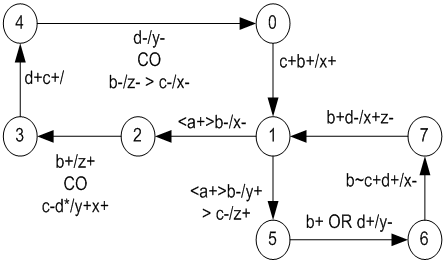 | Figure 6. MBG specification |
3. GMBG Specification
3.1. I/O Sequence Behavior Using Burst Operators
- Consider the timing diagram shown in Figure 7aThis behaviour can be described by both specification, STG and XBM. This behaviour may be described in XBM defining two sequential state transitions activated by the inputs bursts (a+b*/x+y+) and (b+c+/z+) (Figure 7b). Suppose that the input burst c+ is activated immediately after the activation of the output signal y+ as a result there is a violation of the I/O-Mode. The input/output (I/O) operation mode, says in which a new input is accepted as soon as an output transition has finished. If the 3D-tool synthesizes this behaviour, so delay elements should be inserted in the line of the signal c to satisfy the I/O-Mode. This procedure is not tailored for FPGAs. A more efficient solution consists of describing this behaviour through two sequential bursts, but activated immediately (a+/x1+y2+) SEQ (b1+c2+/z+) exactly as the timing diagram showed in Figure 7a. This description creates a limited degree of concurrency between an input c and the output x (Figure 7c), therefore, it operates in the I/O-Mode. This example illustrates the extension of the SEQ operator.
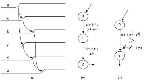 | Figure 7. Specification types: a) timing diagram; b) XBM; c) GMBG (SEQ operator à symbol >) |
3.2. Descriptions in GMBG
- Figure 8 shows some descriptions of benchmark controllers in GMBG that are originally described in STG, but on the other hand, these controllers cannot be described in XBM, because the reduction of concurrency between the signals of input / output is very high, invalidating the interaction with fast environments.
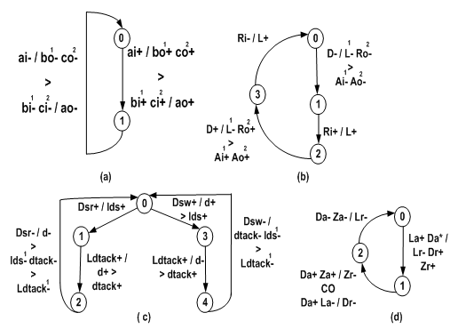 | Figure 8. Benchmarks in GMBG: a) PAR; b) FIFO; c) VME bus; d) A/D Fast |
4. Synthesis Procedure
- Our controllers operate between state transitions in the GFM. In the state transitions with the SEQ operator, the controllers operate in I/O mode. Our method begins from the GMBG specification and the procedure has six steps:1. Behavioural capture using GMBG specification;2. Transformation of the GMBG into a minimum set of MBG Flow Maps (MBG-FMMIN-SET). It should satisfy requirements that solve all conflicts and allow hazard-free logic minimization[10],[12] (see section A);3. Codify the MBG-FMMIN-SET avoiding critical race and with the lowest number of state variables[10];4. Logic minimization (see section B) for each non-input signal (FSET and FRESET);5. Technology mapping for each non-input signal (FSET and FRESET)[28];6. Structural VHDL for each non-input signal (FSET and FRESET)[30].
4.1. Covered Conditions
- Figure 9 shows the MBG-FM (2 mean don’t-care) involving state transition of the TSEQ type. The cells labelled with R in the figures are reserved and they aren’t part of the possible paths (inputs bursts and outputs bursts activated), although they can be used in the logic cover. The set of reserved cells allows each non-input signal to hold a hazard-free logic cover with basic gates.
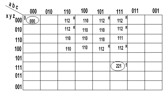 | Figure 9. MBG Flow Map of Figure 7c |
4.2. Logic Hazard-Free Conditions
- For each non-input signal z∈GMBG that has a transition Tj 0→1 described in MBG flow map4, there is a cube that completely covers the paths of all cells of value 1 (minterms). To illustrate the concept of cube, extracted from the state transition 0 → 1 in Figure 9, the cube of the signal x which is CTJ-X(a,b,c,x,y,z)=122220, where 2 is don’t-care. The theory of hazard-free logic minimization for XBM functions (fGFM-XBM) proposed by Nowick in[12] and Yun in[10] is extended to satisfy the Theorem 1 below, for the two-level function fGMBG (FSET-GMBG and FRESET-GMBG) of the feedback RS standard architecture and delay model is unbounded gate delay bounded wire delay (UGBWD).Theorem 1: Two sufficient conditions for the implementation of hazard-free logic circuits in the feedback RS standard architecture (see Figure 5) are: The circuit doesn’t have any reached state, which is covered for more than one cube (product). The reachable states of the circuit that form the sequence of events (0→1...1) or (1→0…0) of a non-input signal should enable only one cube (product).Proof: Let a sum-products function f (FSET-GMBG and FRESET-GMBG) of a non-input signal y ∈ GMBG is hazard-free functional, that presents the transitions TJ,…,TK 0→1 in the respective state transitions J,...,K and are described in the MBG flow table. Condition 1: Let the cubes (products) and CTJ and CTK of function f that completely cover all minterms (cells with value 1) of the respective transitions TJ and TK. If CTj∩ CTk=∅ then the cubes satisfy condition 1. If CTJ∩ CTK≠∅ then there is at least one minterm that is covered by two cubes therefore violates condition 1. If CTJ ⊂CTK then there is only the cube CTJ, therefore satisfies the condition 1. Condition 2: If ∃ CTJ a cube that completely covers the minterms of the transition TJ (J state transition) and is adjacent to the CTK cube of the K state transition, then CTJ∪CTK that generates a cube unique that satisfies the condition 2. Assuming that in the transitions TJ and TK there is the cubes CTJ and CTK not adjacent (CTJ∩CTK=∅) and there is a path between the final states of the transitions of state J to K, so this path the not-input signal is 1→1. As in the J state transition the cube CTJ was activated and following the path until K, also the CTK cube is activated therefore violates condition 2, because there are two cubes activated. As in the feedback RS standard architecture allows that the next transition following the J, in case the CTJ cube being disabled, so never occurs two cubes being activated, therefore satisfies the condition 2 (cqd).The theorem 1 shows that the fGMBG functions obtained are logic hazards-free for the specified multi-burst transitions types {TS, TSEQ, TCO, TS-C}. The logic cover of state transition of the type of the TOR of GMBG needs two cubes, so the delay model does not satisfy UGBWD. The theorem presented for the transition 0→1 is similar for the transition 1→0.
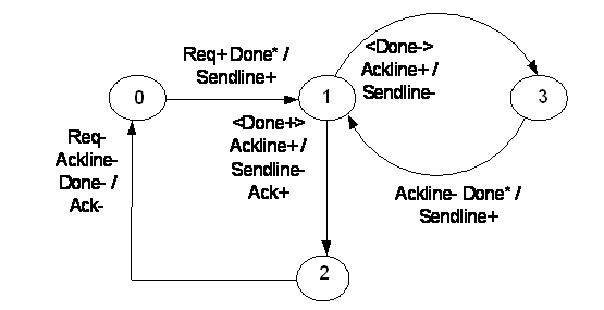
5. Example
- In order to show our method, we used the Input D-Port Controller showed in the Figure 10a. Figure 10b show the version of this controller in GMBG specification (step-1). In this example is applied the extension of SEQ operator .The step-2 transforms the GMBG in two MBG-FM they are respected the requirements. The step-3 codifies the two MBG-Flow Maps using just one state variable (Y signal) (see Figure 11). Figures 12 and 13 show respectively the Karnaugh maps for the Ri signal (Ri-SET and Ri-RESET) (step 4).Ri-SET=Den.y’+Den’.yRi-RESET = Den y Rp’ + Den’ Ai y’ The decomposition wasn’t necessary (trivial technology mapping – step-5). Figure 13 shows the hazard-free logic circuit of the Input D-Port Controller synthesized by our method. The functions are described in structural VHDL (step-6).
 | Figure 10. Specifications: a) STG in[27]; b) GMBG version |
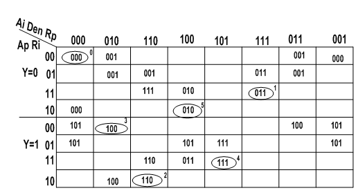 | Figure 11. MBG maps: minimized and codified |
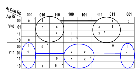 | Figure 12. Karnaugh map: signal Ri-SET → function FSET |
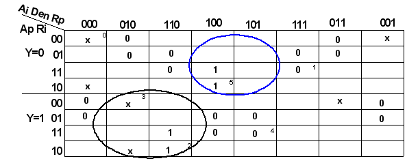 | Figure 13. Karnaugh map: signal Ri → function FRESET |
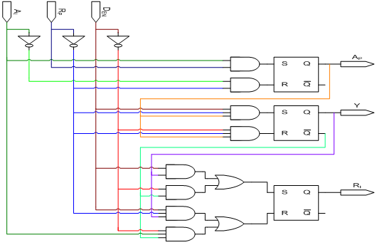 | Figure 14. Logic Circuit: Input D-Port controller |
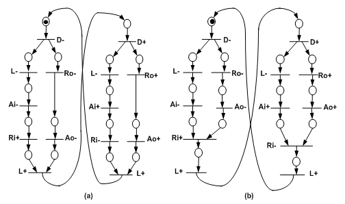 | Figure 15. STGs of FIFO controller: a) original; b) reduced concurrency |
6. Results & Discussion
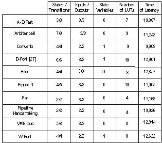
- The strong of STG is to describe concurrency between inputs and outputs, important in the interaction with fast environments. The drawback is to describe decisions (input choices), by example, involving signals LSS, which are important in heterogeneous systems, where STG can explode in the size, becoming very confusing.The strong of XBM is to describe decisions involving signals LSS, concurrency of input signals and output signals. The drawback is to describe concurrency between signals of input and output, and sequence of signals. The GMBG description is compact, not confused and it is familiar to designers of the synchronous digital circuit (based on the state diagram). The GMBG describes several types of concurrency, but still have some limitations. For example the GMBG description of the FIFO controller (Figure 8b) reduced the concurrence of the signal Ri. Figure 15a shows the original STG description of FIFO controller and Figure 15b shows the equivalent FIFO controller depicted in the Figure 8b. Through of timing diagram of a state transition, the Figure 16 shows the capacity of the GMBG in to describe concurrency and sequence. Beister et al. in[31] presents a procedure that transforms STG in XBM. The STG of the Figure 1 could be transformed in two XBM and just one GMBG (see Figure 4). The Table-1 shows ten benchmarks that are described originally in STG and that were transformed in GMBG. The table contents the number of states and state transitions for the MBG transformation as well as the state variables, the number of LUTs and the maximum latency time for each benchmark. These circuits were simulated in the QUARTUS II to the target EP2C35F672C7[30]. The simulations didn’t show any hazard problem and the circuit operated as predicted in its specification. Figure 17 shows the hazard-free waveforms extracted from the simulation of the Input D-Port Controller that the logic circuit is showed in Figure 14.
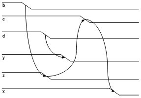 | Figure 16. Timing diagram: state transition 4→0 of Figure 6 |
|
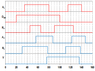 | Figure 17. Timing diagram: input D-Port of Figure 10b |
7. Conclusions
- This paper shows the MBG specification. It describes all signals types of the XBM specification and I/O concurrence with CO and SEQ operators. The extension SEQ operator allows the circuit interacting with the environment in the I/O mode. We also show that multi-burst mode controllers can be implemented on LUT-based FPGA in the BGWD class and using RS latches. For future work we intend to develop a tool for automatic synthesis. And we intend to go further on large asynchronous controllers in FPGA.
Notes
- 1. The 3D-tool synthesizes XBM controllers[10].2. The symbol // means concurrency.3. State transitions without operator are of TS type.4. The treatment is similar to transition 1→0.