-
Paper Information
- Next Paper
- Previous Paper
- Paper Submission
-
Journal Information
- About This Journal
- Editorial Board
- Current Issue
- Archive
- Author Guidelines
- Contact Us
Microelectronics and Solid State Electronics
2012; 1(4): 94-97
doi: 10.5923/j.msse.20120104.04
Low-Power and High-Performance 1-Bit Set Full-Adder
 Abstract
 Reference
 Full-Text PDF
 Full-Text HTML
Anbarasu Paulthurai , Balamurugan Dharmaraj
Assistant Professor, ECE Department, St. Joseph University in Tanzania Dar-Es-Salaam, Tanzania
Correspondence to: Anbarasu Paulthurai , Assistant Professor, ECE Department, St. Joseph University in Tanzania Dar-Es-Salaam, Tanzania.
| Email: |  |
Copyright © 2012 Scientific & Academic Publishing. All Rights Reserved.
Single Electron Transistor (SET), distinguished by a very small device size low power dissipation, high speed and high performance, is one of the most promising nano electronics devices to replace conventional CMOS. The SET technology offers the ability to control the motion of individual electrons in the designed circuits. An adder is very important, both as stand-alone unit and as a basis for other units such as program counters, multipliers, and memory addressing units. In this Full Adder Circuit we are using 24 SET and 14 resistors. The circuit is functioning as required for all the combination of input voltage. This work evaluates the performance of the proposed designs in terms of delay, area, power, and their products by hand with logical effort and through custom design and layout in SET process technology. The results analysis shows that the proposed minority function based full adder implemented in multiplier is better than the conventional multipliers.
Keywords: SET, Full Adder, High-Speed
Cite this paper: Anbarasu Paulthurai , Balamurugan Dharmaraj , "Low-Power and High-Performance 1-Bit Set Full-Adder", Microelectronics and Solid State Electronics , Vol. 1 No. 4, 2012, pp. 94-97. doi: 10.5923/j.msse.20120104.04.
Article Outline
1. Introduction
- The performance of many applications such as digital signal processing depends on the performance of the arithmetic circuits to execute complex algorithms such as convolution, correlation and digital filtering. Usually, the performance of the integrated circuits is influenced by how the arithmetic operators are implemented in the cell library provided to the designer and used for synthesizing. As more complex arithmetic circuits are presented each day, the power consumption becomes more important.The arithmetic circuits grows more complex with the increasing processor bus width, so energy consumption is becoming more important now than ever due to the increase in the number and density of transistors on a chip and faster clock Increasing demand for fast growing technologies in mobile electronic devices such as cellular phones, PDA’s and laptop computers Requires the use of a Single Electron Transistor Full Adder in Nano Technology systems since it is the core element of arithmetic circuits. Decreasing the power supply leads to power consumption reduction.However, lowering supply voltage also increases circuit delay and degrades drive ability of cells designed with certain logic styles. One way of consuming less power is that a circuit operates at extremely low frequency, but it may take a very long time to complete which is in contrast with high speed operation demands. A specific task of our work is to make a comparison of the power consumption of the Full Adders designed with different logic styles. We measured the energy consumption by the product of average power and worst case delay. The power-delay product (PDP) represents a trade-off between two compromising features of power dissipation and circuit latency. Single electron transistor (SET) is a new type of switching device that uses controlled electron tunneling to amplify current. SET is distinguished by a very small device size and ultra-low power dissipation and based on controlling the transport of an individual electron. In 1987, Likharev has proposed a single-electron transistor in which the tunneling of the electrons is controlled by a bias applied at the center electrode[1]. Since then, various solutions have been developed on logic circuits, memory and other circuits. The first single electron inverter, made from two complementary SETs was proposed by Tucker et al. in 1992[2]. This work explained the principles of designing complementary SETs, that corresponds to the PMOS and NMOS transistors, which can be used to design CMOS-style logic.
2. Comparison between CMOS and SET
- The downscaling of complementary metal-oxide semiconductor (CMOS) technology is still in rapid progress and the increase in power consumption has become a major limiting factor in constructing large-scale integrated circuits. Consequently, the single-electron transistor (SET) has attracted considerable attention in recent years because of its potential for high packing density and low power consumption. A variety of useful devices and concepts utilizing the single-electron tunneling features, such as, cellular automata, the binary decision diagram device, and SET logic gates, have been proposed and tested by actual devices. To operate a SET circuit at room temperature, Coulomb islands constituting the circuit should be made extremely small to provide large charging energy that is sufficient to overcome thermal agitation. However, since the operation of a SET is strictly controlled by the amount of charge induced at the center island, reducing capacitances by scaling of a device should be accompanied by increased voltage and current levels. Thus, in contrast to the MOS transistor, the power consumption of a SET increases as the possible operation temperature rises, and the possibility of the integration of above 1011/cm2 is questionable, since on the order of 10−9W will be dissipated per elementary gate at room temperature. In this study, supply-voltage scaling is introduced as a method for reducing the power consumption of SET circuits[8].
3. The Basic Physics of SET
- The main component of SEC is the tunnel junction that can be implemented using silicon or metal-insulator-metal structures, GaAs quantum dots, etc. The tunnel junction can be thought of as a leaky capacitor. For very small tunnel junctions, the movement of only one electron, from one side of the tunnel junction to the other, may produce a noticeable change e/C of the voltage across the tunnel junction. Note that the above C =CJ+C6 where C6 is the equivalent capacitance of the remainder of the circuit, as viewed from the tunnel junction's perspective[3].
4. Single Electron Tunneling
- The principals of single-electron electronics have been presented in many publications[6, 7]. Summarizing, in the single-electron technology, the circuits consist of conducting islands, tunnel junctions, capacitors, and voltage sources. The islands are arbitrarily connected with tunnel junctions, capacitors and voltage sources. The basic component of single electron tunneling technology is the tunnel junction. A tunnel junction can be considered as two conductors separated by a thin layer of insulating material. A tunnel junction and its schematic diagram are shown in Fig.1. It is characterized by a capacitance Cj and a resistance Rj, each of which depends on the physical size of the tunnel junction and the thickness of the insulator. The fundamental principle of SET devices and circuits is the Coulomb blockade[5].
5. Single Electron Transistor
- The single electron transistor or SET is type of switching device that uses controlled electron tunneling to amplify current. A SET is made from two tunnel junctions that share a common electrode. A tunnel junction consists of two pieces of metal separated by a very thin insulator. The only way for electrons in one of the metal electrodes to travel to the other electrode is to tunnel through the insulator. Since tunneling is a discrete process, the electric charge that flows through the tunnel junction flows in multiples of e, the charge of a single electron[3].
5.1. Structure of Single-Electron Transistors
- Single-electron transistors (SETs) are three-terminal switching devices, which can transfer electrons form source to drain one by one. The schematic structure of SETs is shown in Figure 1. As shown in the figure, the structure of SETs is almost the same as that of MOSFETs. However, SETs have tunneling junctions in place of pn-junctions of the MOSFETs and a quantum dot in place of the channel region of the MOSFETs[1].
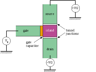 | Figure 1. Schematic structure of SET |
6. Adders
- Parallel multipliers are well known building blocks used in digital signal processors as well as in data processors and graphic accelerators. However, every multiplication can be replaced by shift and add operations. That is why, the adders are the most important building blocks used in DSP’s and microprocessors. The constraints they have to fulfill are area, power and speed. The adder cell is an elementary unit in multipliers and dividers. The aim of this section is to provide a method to find the computational power by starting from the type of adder. There are many types of adders but generally they can be divided in four main classes:• Ripple carry adders (RCA);• Carry select adders (CS);• Carry look-ahead adders (CLA);• Conditional sum adders (CSA). The starting point for any type of adder is a full-adder FA. The discussion for this adder can be generalized for every type of adders. The outputs SUM and CARRY depend on the inputs a, b and c as:An established method for computing S and Co isS = (A ⊕ B ⊕ Ci), Co = (A & B) + (A & Ci) + (B & Ci),Where, & for logic and, + for logic or, and ⊕ for logic xor.
7. 1-Bit Set Full-Adder
- The 1- Bit SET Full-adder is a basic arithmetic block which has three inputs (the addend A (1-bit precision), the augend B (1-bit precision), and the carry-in Ci) and two outputs: the sum S, and the carry-out Co. The 1- Bit SET Full-adder consist of 14 PSET and 14 NSET Transistor. The supply voltage Vdd is constant and its value is 25mV. The voltage sources V1, V2 and V3, shown in Fig. 1, are the inputs (a, b and c respectively) of the full-adder and it can take only two values 0.0V which corresponds to the logic `0', and 25mV which corresponds to the logic `1'. The input voltage V1(A)is applied to PSET 1,4,7,10 and NSET of 21,18,24,26 through gate, input voltage V2(B) is applied to PSET 2,3,5,14 and NSET of 17,19,20,22 through gate, and the input voltage V3(C) is applied to PSET 6,8,13 and NSET of 15,16,28 through gate. The output signals of the full-adder sum are taken from source of PSET 9 and drain of NSET 27, and N6, and the Carry is taken from source of PSET 11 and drain of NSET 25. The presence of positive charge corresponds to logic `1', whereas no charge corresponds to logic `0'.As shown in Fig. 2.
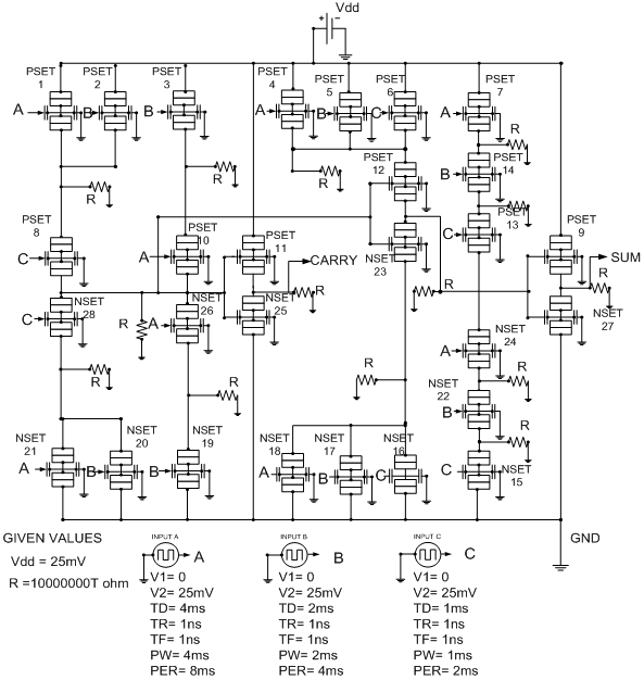 | Figure 2. Internal Circuit of 1-Bit Set Full-Adder |
8. Simulation Results
- The logic operation of the full-adder is shown in fig 3. In this first 3 rows show the time variation of the input V1 and V2, respectively. The piecewise constant and apply all possible combinations of logic ‘0’ and ‘1’ to the circuit. The remaining 2 rows are show the ouput sum and carry respectively. When we applied input voltage[0 0 1] then we get sum is logic ‘1’ and carry is logic ‘0’. When we applied input voltage[0 1 1] then we get sum is logic ‘0’ and carry is logic ‘1’. When we applied input voltage[0 0 0] then we get the both sum and carry is logic ‘0’.
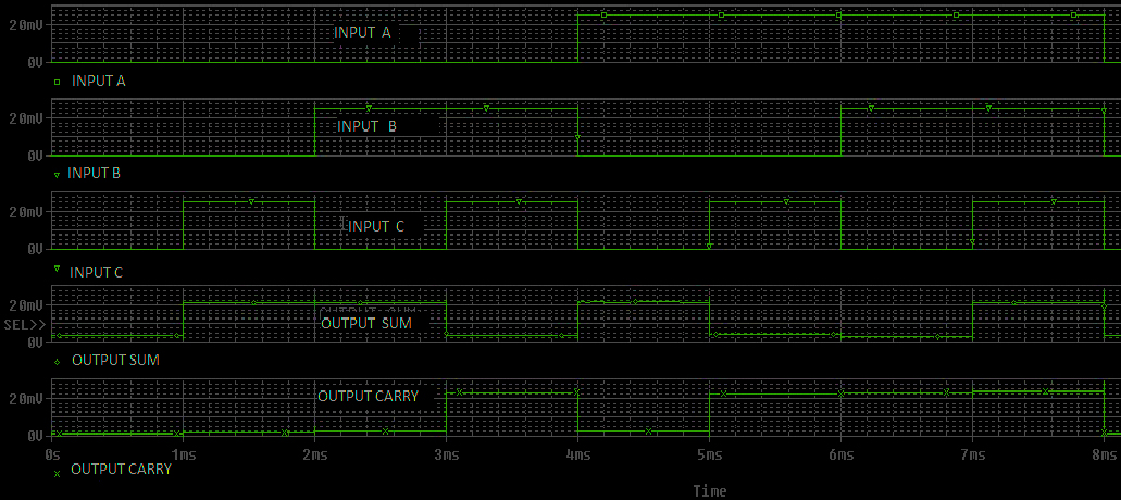 | Figure 3. Simulated input (A B C) and Simulated output (SUM & CARRY) |
9. Conclusions
- The design and operation of full adder is presented in this paper. Truth table is achieved for the operation of SET function based adder and the circuit is designed using Orcad Capture. Comparison is made for the efficient full adder by designing in various technologies. Outputs are verified for the input set and the performance metrics of the efficient full adder are measured and tabulated. 1 bit SET full adder shows 55% reduction of power consumption. Area, Delay and power delay product (PDP) are reduced than their conventional adders. As technology scaling is increased possibility for high reduction in power dissipation and area. So 1 bit SET full adder realizations can be considered as a best choice for the multipliers.
Future Work
- Further this multiplier can be implemented in filters for image processing applications. Due to the increase in speed of multiplier and high reduction in power dissipation it can be used for DSP applications.
ACKNOWLEDGEMENTS
- I would like to thank my friends and my faculty members without whom this Journal would have been a distant reality. I also extend my heartfelt thanks to my family and well-wishers.