Messaadi Lotfi , Dibi Zohir , Smail Toufik
Department of Electronics, University of Batna, Advanced Electronic Laboratory (LEA), Batna, 05000, Algeria
Correspondence to: Messaadi Lotfi , Department of Electronics, University of Batna, Advanced Electronic Laboratory (LEA), Batna, 05000, Algeria.
| Email: |  |
Copyright © 2012 Scientific & Academic Publishing. All Rights Reserved.
Abstract
This paper presents a SiC Schottky diode model including static and dynamic features implemented as a parameterized block constructed from SPICE Analog Behavioral Modeling (ABM) controlled sources. The parameters for this block are easy to extract, even from readily available diode data sheet information. This model can easily simulate the diode’s reverse recovery and power losses behavior over all temperatures from 0℃ to 175℃.
Keywords:
Power Diode, Silicon Carbide Schottky (SiC), Reverse Recovery, Modeling, PSpice, Analog Behavioral Modeling (ABM), Temperature Effect
Cite this paper:
Messaadi Lotfi , Dibi Zohir , Smail Toufik , "Macromodeling with Spice of SiC Schottky Diode", Microelectronics and Solid State Electronics , Vol. 1 No. 4, 2012, pp. 85-93. doi: 10.5923/j.msse.20120104.03.
1. Introduction
With increasing global emphasis on energy efficiency, improved power devices are critical to the development of the next generation of power systems. Increasing the efficiency of power conversion systems produces multiple benefits. Increasing the efficiency of a system has the obvious benefit of increasing the power output of the system, and it also has the benefit of reducing the amount of waste heat being generated, leading directly to a reduction in the size, weight and complexity of the cooling system. Further decreases in size and weight can be achieved by operating the system at a higher frequency, thereby reducing the number and mass of passive components.Schottky Barrier Diodes (SBDs) are currently the most mature SiC devices and are delivered by several manufacturers (e.g. Cree, Infineon, Sensitron)[1]. SiC Schottky diodes exhibit very attractive features: fast switching and high values of reverse voltage ratings – impossible to simultaneously achieve by silicon- based diodes. They are also potentially able to operate in the range of very high ambient temperatures and power densities. The forward current, reverse voltage and junction temperature rating approach 50 A, 2500V and 250℃ appropriately .The operation of SiC devices in the wide range of ambient temperature have been studied by many authors, and it is believed that the ambient temperature limit for their operation may, in the future, exceed 600℃[2-3] For all that, the need of suitable models to use for circuit and system design becomes evident for such parts. Ideally, these models should include both static and dynamic features and also, due to the high temperature operation capability of devices, thermal modeling and especially self heating effects that can substantially affect operation.In the following paragraphs, we will build the macromodel (ABM) as one block for static and dynamic response that will finally be joined together into a single model in the Spice library.
2. Diode Characteristics
2.1. Static Characteristic
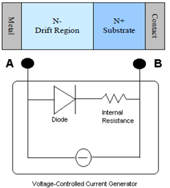 | Figure 1. Electric Schottky diode Model |
Fig.1 shows the original Schottky Diode model we have implemented. It is composed of a voltage controlled current generator in parallel to the original SPICE diode[4]. The aim of this current generator is to provide a better accuracy in the reverse I-V characteristic. The I-V and reverse current are among the static characteristics of the device. Due to higher level of majority carrier injection in Si diode, this causes a lower voltage drop and hence smaller capacitance to bias the junction for turn-on process. This is the only advantage of Si diode compared to SiC. Here, SiC diode requires a higher voltage to forward bias the device[5-8]. A part from that, SiC diode can handle larger reverse voltage as compared to Si.The forward I-V characteristics will be modeled by means of the standard piece-wise linear (PWL) model[9] featuring a D.C. voltage V0 and a series resistance Rd as follows: | (1) |
Temperature dependence for V0 and Rd is introduced at this point as: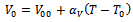 | (2) |
 | (3) |
Where V0 temperature dependence is assumed linear, which is a good fit in practice, and series resistance is fitted by a power law. If we want a simpler linear model we can make n =1. However, a better fit is generally achieved if n has a value between 2 and 3. For practical purposes, the value 2 can be forced with sufficient approximation. T0 is the reference (ambient) temperature.Substituting (2) and (3) into (1) we get for the diode forward drop, including temperature variation: | (4) |
This constitutes the model equation. Note that the way equations (2), (3) and (4) are stated, αV and αR have dimensions of V /℃ and Ω / (℃) n. This is consistent with the way parameters are extracted from data sheet or measurements.
3. Dynamic Characteristic
The characteristic that changes with time is inherited in both devices. Si and SiC diodes are compared in terms of the reverse recovery time, reverse recovery current and corresponding switching losses. The comparisons in dynamic characteristics between two devices are tabulated in Table 1. The SiC and Si diodes used are of part number SDP04S60 and SB30-03F respectively[10-11].| Table 1. Comparison of Dynamic Characteristics |
| | Characteristics | SiC Schottky(SDP 04S60) | Si Schottky(SB30-03F) | | Reverse Recovery Time | Unchanged with temperature variation | Increases as temperature increases | | Reverse Recovery Current | Negligible | Increases as temperature increases | | Switching Losses | Low | Slightly higher |
|
|
Table 1 show that SiC diode has advantages in all dynamic characteristics. Si diode suffers from higher reverse recovery current and switching losses. This clearly indicates the additional carbide substance in the device may improve switching speed and reduce power dissipation.
3.1. Reverse Recovery
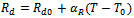
Reverse recovery is one of the properties in a diode. It can be a factor in determining the efficiency of the applications. When a diode has been conducting in a forward bias long enough for it to establish steady state, there will be charges due to the presence of minority charge carriers. This charge must be removed to block in reverse direction[12-14]. | Figure 2. Reverse Recovery Current Characteristic |
The characteristic of reverse recovery current experienced by a diode is represented in Figure.2 above. trr represents the reverse recovery time, Irr is the peak reverse current whilst ta is the transition time due to charge stored in depletion region of the p-n junction. tb is the time for the current to relax to zero. The peak reverse recovery current depends on the falling rate of change in current during turn-off. In SiC diode, there will be less or none reverse recovery current due to its ability to immediately remove stored charge. However, there are differences observed during the recovery from the peak values. This is merely reflected from different device’s fabrication techniques. Normally, in SiC, the rising currents rate to zero takes a longer time (trr) as shown in part (a) in Figure 2. This eventually reduces the turn-off speed. In other SiC type, the speed can also be slightly faster due to smaller tb but with the cost of higher dissipation. This can be seen in part (b) as oscillation exists during the end stage of turn-off time. In addition, if the falling current rate during the beginning of turn-off time is high as in the case of non-schottky diode, the reverse current would also be high, leading to both high power dissipation and lower in turn-off speed[15].
4. SPICE Modeling
Analog behavior modeling (ABM) is utilized extensively in this model to represent the conductance of the diode based on equations presented in the first chapter. ABM itself is a powerful tool available in most SPICE software packages enabling time and frequency domain evaluation of equations or look up tables[16]. Some packages provide block diagram components simplifying the modeling process. The proposed charge control model was implemented using ABM block diagram components as shown in Figure 3.Taking advantage of existing stability, only the modified charge controlled equation was added to the native diode model available in the standard SPICE library. The model is a function of temperature and with a few parameter changes can easily represent a new JBS SiC diode at the respective temperature. The new diode model shown in figure 4 was packaged in a single part for quick archiving into the existing library.The first step towards a model is extracting the parameters that describe the behavior of the diode. For all semiconductors, temperature has a significant effect on the material's conductive properties. Silicon carbide increases resistance with increasing temperature and this is observable in the curve trace. At elevated temperatures, the carriers at the junction become excited lowering the junction voltage[17]. These two phenomenons are demonstrated from the collected data and presented in Figure 4 illustrate the thermal influence on conductivity.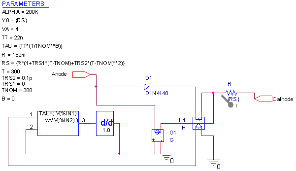 | Figure 3. SPICE ABM static and dynamic SiC Schottky Diode Model |
 | Figure 4. SPICE symbol Diode Model inserted in spice library |
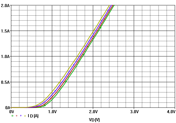 | Figure 5. Forward characteristic at T= 25℃, 75℃, 125℃ and 175℃ (yellow to green) |
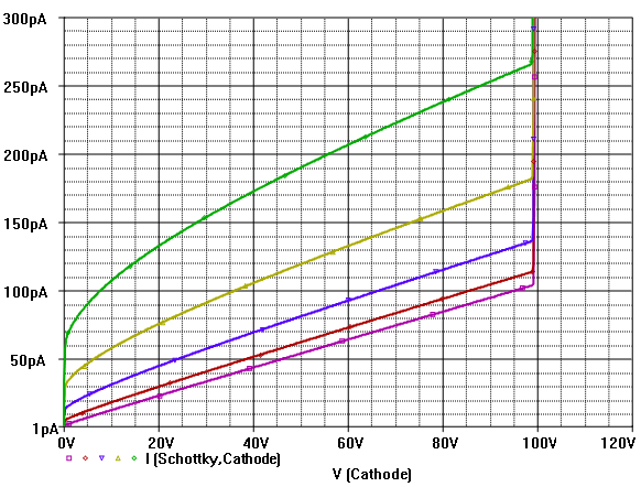 | Figure 6. Reverse voltage characteristics of SiC schottky diode at T=300°C,350°C,400°C,450°C and T=500°C (Purple to Green) |
5. Test Circuit Simulation
The test circuit used for the Pspice simulation of this model is shown in figure. 7 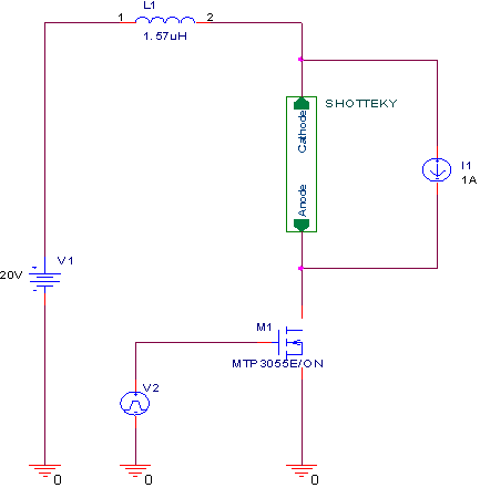 | Figure 7. The test circuit used for simulation |
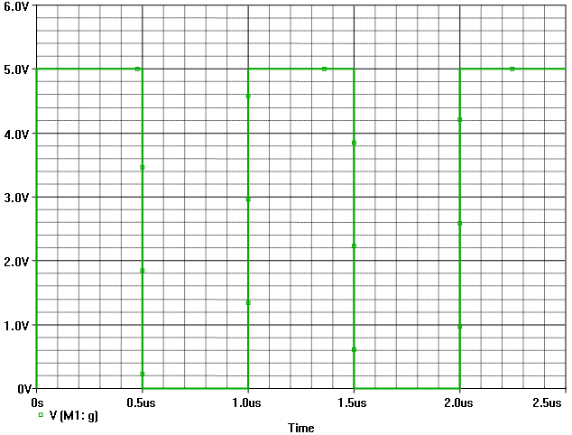 | Figure 8. V2 (Vpulse) Signal |
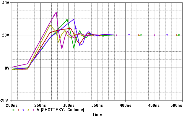
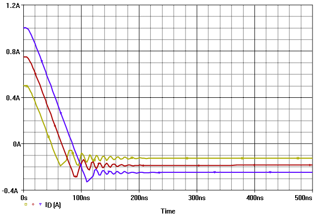 | Figure 9. Turn-off Reverse Recovery Current of SiC Diodes for I1 = 0.5A, 0.75 A and 1A (yellow to blue) |
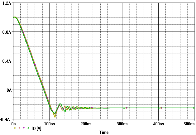 | Figure 10. Turn-off transient for I1= 1 A and T = 25℃, 75℃, 125℃ and 175℃ |
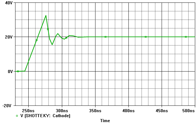 | Figure 11. Forward recovery simulations of SiC Shottky |
 | Figure 12. Forward recovery simulations of SiC at T=25℃, 75℃, 125℃, 175℃ (purple to blue) |
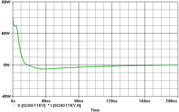 | Figure 13. Power Loss during FET Turn-On |
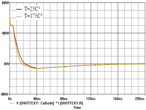 | Figure 14. Power Loss during FET Turn-On for T=25℃ and T=175℃ |
6. Conclusions
A model for SiC Schottky Barrier Diodes based on SPICE ABM has been presented. This model not only described static and dynamic characteristics of SiC Schottky power diodes, but also reflects their dependence on temperature. Thus, they are very useful and effective to estimate the power losses of SiC Schottky diodes and to predict device temperatures. The model was also used to estimate the efficiency of a Si IGBT/SiC Schottky diode hybrid inverter.
ACKNOWLEDGEMENTS
The author would like to thank the director of Advanced Electronic Laboratory (LEA) Professor. N. Bougechelle for his great help.
References
| [1] | Anant Agarwal and Sei-Hyung Ryu” Status of SiC Power Devices and Manufacturing Issues” CS MANTECH Conference, April 24-27, 2006, Vancouver, British Columbia, Canada. |
| [2] | Francesc N. Masana”SiC Schottky Diode Electrothermal Macromodel” Microelectronics Reliability, Vol. 47, No 12, pp 2122-2128, Dec. 2011. |
| [3] | S. Duman, E. Gür, S. Dogan and S. Tüzemen. “Temperature dependent capacitance and DLTS studies of Ni/n-type 6H-SiC Schottky diode”. Current Applied Physics, Vol 9, pp 1181-1185, 2009. |
| [4] | S.M. Sze, Physics of semiconductor devices", Ed. Wiley & Sons, New York, 1981. |
| [5] | W. JANKE, A. HAPKA_, and M. OLEKSY” DC characteristics of the SiC Schottky diodes” bulletin of the polish academy of sciences technical sciences, vol. 59, no. 2, 2011. |
| [6] | R.L. Libby, T. Ise and L. Sison, “Switching Characteristics of SiC Schottky Diodes in a Buck DC-DC Converter” Proceedings in. Electronic and Communications Engineering Conference,(Available:http://www.dilnet.upd.edu.ph/~irc/pubs/local/libbyswitching.pdf), Oct. 2006. |
| [7] | B. Ozpineci, M.S. Chinthavali, and L.M. Tolbert. “A 55 kW Three- Phase Automotive Traction Inverter with SiC Schottky Diodes”. IEEE Conf. on Vehicle Power and Propulsion, pp 541-546, 2005. |
| [8] | A.P. Malvino, “Transistor Circuit Approximation”, McGraw-Hill, Inc., 3rd Ed., 2007(Available: http://www.eng.uwi.tt/depts/elec/staff/rdefour/ee33d/s2_rrchar.html) |
| [9] | Michael D. Reid, Simon D. Round and Richard M. Duke “Modelling the Temperature Dependent Reverse Recovery Behaviour of Power Diodes” Kluwer Academic Publishers, April,2011 |
| [10] | N. Z. Yahaya, F. H. Ramle” Simulation and Analysis of Si Schottky Diode Family in DC-DC Converter” International Journal on Electrical Engineering and Informatics - Volume 1, Number 2, 2009 |
| [11] | Zhu, L.; Chow, T.P.: “Analytical Modeling of High-voltage 4H-SiC Junction Barrier Schottky (JBS) Rectifiers”. IEEE Transactions on Electron Devices, Vol. 55, No. 8, August 2008, pp. 1857-1863. |
| [12] | Ali Dastfan”A New Macro-Model for Power Diodes Reverse Recovery” Proceedings of the 7th WSEAS International Conference on Power Systems, Beijing, China, September 15-17, 2007. |
| [13] | G. Majumdar and T. Oomori, “Some key researches on SiC device technologies and their predicted advantages”, Power Semiconductors 6, 18–229 (2009). |
| [14] | F. Mohammed, M.F. Bain, F.H. Ruddell, D. Linton, H.S. Gamble and V.F. Fusco, “A Novel Silicon Schottky Diode for NLTL Applications”, IEEE Transactions on Electron Devices, vol. 52, issue. 7, pp. 1384-1391, July. 2005. |
| [15] | W. Janke and A. Hapka, “Inluence of series resistance on thermal limitations of SiC Schottky diodes”, Int. Conf. 5th Wide Bandgap Materials – Progress in Synthesis and Applications 1, CD-ROM (2010). |
| [16] | Janusz ZARĘBSKI, Jacek DĄBROWSKI ” Electrothermal Model of SiC Power Schottky Diodes” PRZEGLĄD ELEKTROTECHNICZNY (Electrical Review), ISSN 0033-2097, R. 87 NR 10/2011. |
| [17] | Ramshaw R. S., “Power Electronics Semiconductor Switches”, Chapman & Hall, 1993. |
 Abstract
 Reference
 Full-Text PDF
 Full-Text HTML