Ki-Jin Kim , Sanghoon Park , K. H. Ahn
Convergence Communication Components Research Center, Korea Electronics & Technology Institute, Seongnam-siGyeonggi-do, 463-816, Korea
Correspondence to: Ki-Jin Kim , Convergence Communication Components Research Center, Korea Electronics & Technology Institute, Seongnam-siGyeonggi-do, 463-816, Korea.
| Email: |  |
Copyright © 2012 Scientific & Academic Publishing. All Rights Reserved.
Abstract
Thispaper presents a design of 60 GHz active phase shifter for next generation mm-Wave WPAN using 90 nm TSMC CMOS technology.The vector modulator based phase shifter is chosen as a prototype because it provides accurate resolution over wide bandwidth. The phase shifter is controlled by binary current weighted 5-bit DAC. A miniaturized Marchand balun and a 2-stage poly phase filter are used to generate differential I/Q signal from mm-Wave single input. The three CS (Common Source) amplifiers are adopted for providing enough gain to the proposed circuit. The measured phase resolution of the circuit is 11.250 with maximum 30 phase error. The peak gain from the S-parameter measurement is 9 dB while drawing 50 mA from a 1.2 V supply.
Keywords:
Phase Shifter, MarchandBalun, WPAN, Vector Modulator
Cite this paper:
Ki-Jin Kim , Sanghoon Park , K. H. Ahn , "Design of 60 GHz Vector Modulator Based Active Phase Shifter", Microelectronics and Solid State Electronics , Vol. 1 No. 4, 2012, pp. 81-84. doi: 10.5923/j.msse.20120104.02.
1. Introduction
Recently 60 GHz ISM frequency band with 7 GHz bandwidth has been released for next generation WPAN(Wireless Personal Area Network) and wireless high-definition streaming.Due to the large bandwidth several Gbps wireless communication will be possible in near future. However the channel condition of the 60 GHz is extremely poor so the transmitted power is severely attenuated in air. Thus it is necessary to use phased array system which enables to transmit and receiverelatively high power using multiple transmitters and antennas.Phase shifters in the phased array system are the key components because the beam pattern of the antenna is artificially adjusted by the specific combination of the output signals of each phase shifter.There are several ways of implementing phased array system. In[1-2], the IF and digital arrayed systems were introduced. In these papers, the phase shifters were located at the IF stage or after the ADC circuit. Therefore, they used a lot of array components such as LNA, Mixer, AGC, Filter, and ADC. Thus choosing afore-mentioned structures as a prototype requires large chip area and power consumption.In[3], LO (Local Oscillator) phase shifting was proposed. It is good architecture comparing to previous works however, it still needs the mixer arrays and the complex local generation circuits. The RF phase shifting architecture was proposed in[4]. The RF phase shifter combines arrayed RF signal directly at the RF front end of the transceiver. So the required array components are minimized to only RF circuits. In this paper, the 60 GHz vector modulator based active phase shifter is presented as a RF phase shifter using 90 nm CMOS TSMC technology. It consists of CS (Common Source) amplifiers, Marchand balun, poly phase filter, 5 bit digitallycontrolled vector modulator. The proposed circuit shows 11.250 phase resolution with 30 phase error and 9 dB peak power gain under 1.2 V supply.
2. Proposed Structure of the Phase Shifter
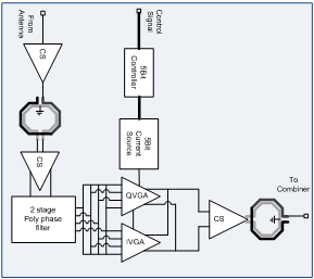 | Figure 1. The block diagram of the proposed phase shifter |
In this section, the structure of the proposed phase shifter is illustrated. The overall block diagram is depicted in Fig. 1. The input CS amplifier provides input matching and gain to the phase shifter. To generate differential I and Q signal,aMarchand balun and a 2-stage poly phase filter are adopted.There are various types of RF phase shifter: switched delay[5], loaded line[6], and vector modulator based phase shifter[7]. Considering low and equal insertion loss and phase resolution across 7 GHz frequency, thevectormodulator based phase shifter is chosen in this paper. At the last stage of the circuit anotherMarchand balun is placed for converting differential signal to single signal.
2.1. Common Source Amplifier
Fig. 2 shows the structure of the input common source amplifier for providing gain and for matching input impedance of the circuit. The input matching structure consists of two inductors.The transmission line in the source is used for source degeneration. The L1 shunt inductor not only serves as a matching component but also as an ESD protector since it provides much lower impedance path than the impedance of the input L2.The on chip transmission lines are also used as matching components. The S-parameter results of the transmission line from the 3-D simulation are transformed into its equivalent circuit (Fig. 2) by the equation (1-3). 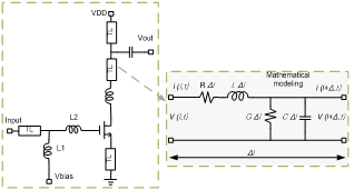 | Figure 2. The input CS amplifier and modeling of the transmission line |
 | (1) |
 | (2) |
 | (3) |
After aforementioned transformation, the transmission lines can be used in the manner of simple scalable components.
2.2. MarchandBalun
The advantages of using Marchand balunas a prototype are the no DC power consumption and wideband frequency responsewith a low insertion loss. Thus the on chip miniaturized Marchand balun is adopted here for single to differential conversion or vice versa. Fig. 3 shows the structure of the balun. Single port 1 is connected with half wave length line with its load open and differential port 2 and 3 are connected with quarter wave length line with their load short. One of the great characteristics of the Marchandbalun is that the coupling coefficient k of the coupled lines can be determined by the termination impedance ZL. As the ZL increases, the required value of the k decreases. Thus the parallel coupled structure which has a low coupling characteristic can be designed with coupling coefficient 0.6 and ZL 200 Ω. To minimize the balun size, the winding structure is adopted. The simulation S-parameter results are plotted in Fig. 4 with the minimum insertion loss 1.16 dB. | Figure 3. The proposed Marchandblaun and its equivalent structure |
 | Figure 4. Simulated result of the proposed balun |
2.3. Polyphase Filter
To drive vector modulator, differential I and Q signals are required. The Hybrid coupler was generally used for quadrature generation even on chip condition. However it takes large chip area and needs additional baluns for differential output. All pass filter type quadrature generation was successfully implemented in mm-Wave application. But the mismatches caused by the loading effect make all passfilter design unattractive in 60 GHz frequency.The passive poly phase filter has been widely used forquadrature generation due to its small area and simple design. | Figure 5. The structure of the two-stage poly phase filter |
The poly phase filter configuration as shown in Fig. 5 has an inherent 900 phase different at their output over all frequencies. The only matter is amplitude mismatch. For the wide band operation, two stage poly phase filter is adopted. Nevertheless it shows considerable insertion loss.
2.4. Vector Modulator
For the operation of vector modulator, differential I and Q input signal are required. The vector modulator is the core building block for the phase shifter. The I/Q signals with variable amplitude and polarity are combined to generate designated phase. Therefore the vector modulator consists of I/Q VGAs (Variable Gain Amplifiers) with polarity inversion capability.Fig. 6 shows the detail schematic of the I or Q VGA. To produce output of the vector modulator, I and Q VGA amplify the input signals and produce constant output like the equation (4). So the required equation of the each VGA is equated in (5).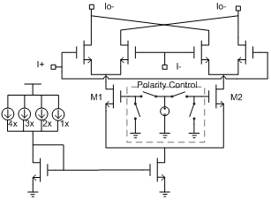 | Figure 6. The VGA structure |
There is a linear trans-conductance (gm) region in the transistor where the current density of the transistor is low. We choose this low current density region as a bias point of the I and Q VGA to satisfy the equation (5) with the binary weighted current source.  | (4) |
 | (5) |
4 bit digital control signals controls the I and Q VGA’s gm and the last bit controls the polarity of the VGA by switching polarity control block shown in Fig. 6. The polarity control block makes the current only flow either the transistor M1 or M2. By the differential nature, the polarity of the VGA output is changed in this manner.The output of the I and Q VGA are current. Thus the transmission line inductors are usedfor signaladdition.
3. Measurement Results
The circuit was fabricated in a 90 nm TSMC CMOS process with ft and fmax of 120 GHz and 150 GHz respectively. The backend features 9 copper layers with the top thick metal 3.3μm. The die photo of the phase shifter is shown in Fig 7. It occupies an area of 1 x 0.76 mm2 including probe pads. The proposed circuit was measured by on wafer probe system to reduce parasitic interconnection effects. Fig. 8 shows the measured S-parameter results. It shows 9 dB peak gain with little center frequency shift. The simulated peak gain is 14 dB. The gain reduction was caused by input and output mismatching.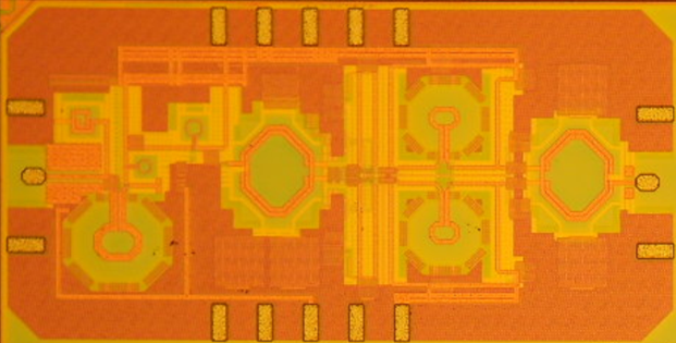 | Figure 7. The photograph of the phase shifter |
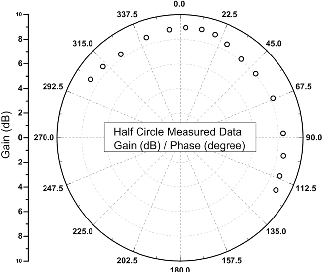
The measured gain and phase characteristics are plotted in Fig. 9 at the 57 GHz frequency. The remained half feature might be same because the symmetrical design. The measured result shows that the 5 bit resolution is satisfied with the maximum phase error 30.In the Table I, the key results of this work are summarized and compared with previous works.The phase shifter presented in this work shows high resolution and gain at 60 GHz frequency.| Table 1. Result summaries with previous works |
| | Ref | Frequency(GHz) | Resolution(degree) | Gain(dB) | Technology | | This work | 60 | 11.25 | 9 | 90nmCMOS | | [5] | 12 | 11.25 | -14.5 | 0.18μmCMOS | | [6] | 12 | 22.5 | 3.5 | 0.18μmCMOS | | [7] | 26 | 22.5 | -3 | 0.13μmCMOS | | [8] | 34 | 22.5 | 1 | 0.12μmBiCMOS |
|
|
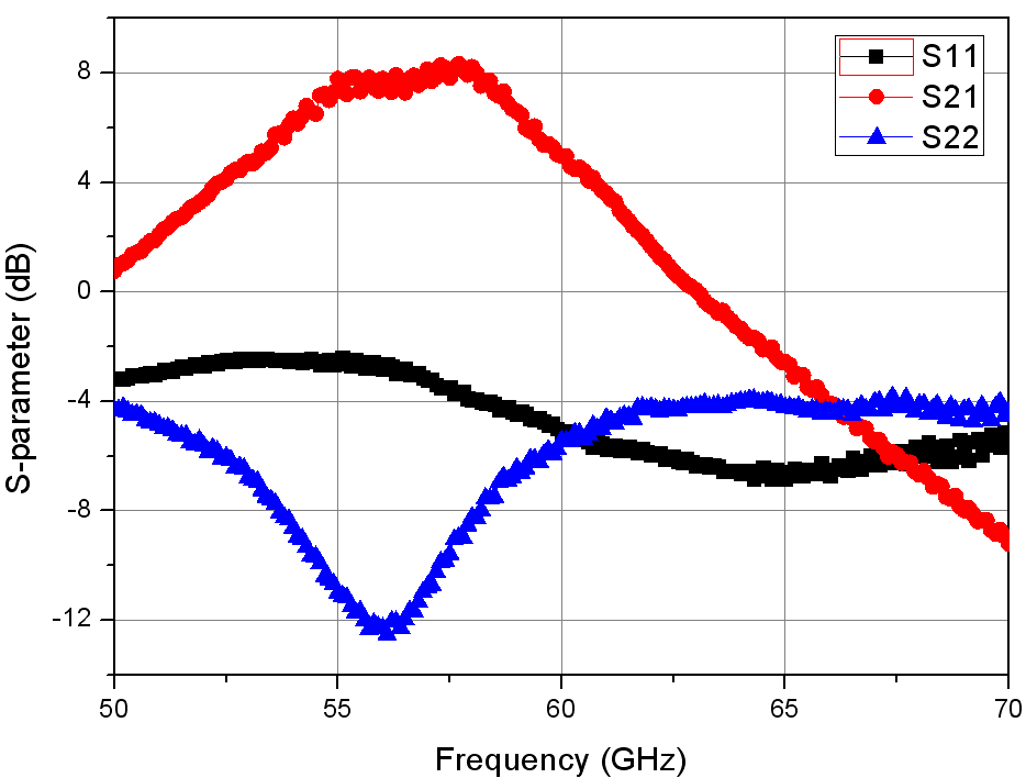 | Figure 8. The measured S-parameter results |
 | Figure 9. The characteristics of gain and phase |
4. Conclusions
A vector modulator based active phase shifter was proposed and its results were measured by on chip wafer probing. The measured results showed that the proposed circuit has 9 dB gain and 11.250 phase resolution. The maximum phase error over the whole frequency is 30 which means that the proposed circuit satisfied the 5 bit resolution. Thus the presented paper can be a good phase shifter solution for mm-Wavearray system.
ACKNOWLEDGEMENTS
This work was funded by Ministry of Knowledge Economy and the project name is “Design of 60GHz Analog Beam Former”. Fabrication was provided by TSMC. We thank Korea Advanced Institute of Science and Technology for their support in design and test.
References
| [1] | S. Raman, N. Baker, and G. Rebeiz, “A w-band dielectric-lens-based integrated monopulse radar receiver,” IEEE Trans. Microwave Theory Tech., vol. 46, no. 12, pp. 2308-2316, Dec 1998. |
| [2] | R. Miura, T. Tanaka, I. Chiba, A. Horie, and Y. Karasawa, “Beamforming experiment with a dbf multibeam antenna in a mobile satellite environment,” IEEE Trans. Antennas Propagat., vol. 45, no. 4, pp. 707-714, Apr 1997 |
| [3] | H. Hashemi, X. Gaun, A. Komijani, and A. Hajimiri, “A 24-GHz SiGe Phased-Array Receiver Lo Phase-Shifting Approach,” IEEE Trans. Microwave Theory Tech., vol. 53, no. 2, pp. 614-626, Feb 2005. |
| [4] | Tiku Yu, Gabriel M. Rebeiz, “A 22-24 GHz 4-Element CMOS Phased Array with On-Chip Coupling Characterization,” IEEE Journal of Solid State Circuits., vol. 43, no. 9, pp. 2134-2143, Sep 2008. |
| [5] | D. Kang, et al, “Ku-band MMIC Phase Shifter Using a Parallel Resonator with 0.18um CMOS Technology,” IEEE Trans. On MTT, Jan 2006 |
| [6] | D. Kang, et al, “A 4-bit CMOS Phase Shifter Using Distributed Active Switches,” IEEE Trans. on MTT, July 2007. |
| [7] | K. Koh, et al, “A 0.13um CMOS Phase Shifters for X-, Ku-, and K band Phased Arrays,” IEEE JSSC, Nov, 2007. |
| [8] | B. Min, et al, “Ka Band BiCMOS 4-bit Phase Shifter with Integrated LNA for Phased Array T/R Module,” IEEE MTT-S 2007 |
 Abstract
 Reference
 Full-Text PDF
 Full-Text HTML