Jhin-Fang Huang 1, Yen-Jung Lin 1, Kun-Chieh Huang 1, Ron-Yi Liu 2
1Department of Electronic Engineering, National Taiwan University of Science, Technology, Taipei, Taiwan
2Chung-Hwa Telecommunication Laboratory, Chung-Hwa Telecommunication Inc., Taoyuan, Taiwan
Correspondence to: Jhin-Fang Huang , Department of Electronic Engineering, National Taiwan University of Science, Technology, Taipei, Taiwan.
| Email: |  |
Copyright © 2012 Scientific & Academic Publishing. All Rights Reserved.
Abstract
A continuous-time (CT) sigma-delta (ΣΔ) modulator clocked at 128 MHz with a hybrid active-passive loop filter is presented for WCDMA applications. The proposed 5th-order loop filter architecture mainly consists of two passive integrators and three active integrators. To erase the summation amplifier used in the chain of integrators with weighted feedforward summation (CIFF) topology, the capacitive feedforward structure is employed. In addition, local feedback resistors form the bridge-T network to reduce the chip area. The prototype chip is fabricated with TSMC 0.18 μm CMOS technology. Under the supply voltage of 1.8 V, measured results have achieved the best FOM of 2.67 pJ/conv, a dynamic range of 62 dB, a SNDR of 60.26 dB, an ENOB of 9.72 bit, IM3 of -48 dB and a power consumption of 9 mW over a 2 MHz signal bandwidth. Including pads, the chip area is 0.642 (1.07 x 0.6) mm2.
Keywords:
Sigma-Delta Modulator, ΣΔ Modulator, WCDMA, CIFF
Cite this paper:
Jhin-Fang Huang , Yen-Jung Lin , Kun-Chieh Huang , Ron-Yi Liu , "A Continuous-Time Sigma-Delta Modulator with a Hybrid Loop Filter and Capacitive Feedforward", Microelectronics and Solid State Electronics , Vol. 1 No. 4, 2012, pp. 74-80. doi: 10.5923/j.msse.20120104.01.
1. Introduction
With increasing development of wireless communication systems, there is a large demand in the wireless communication for analog-to-digital converters (ADCs) that require signal bandwidths of several mega-hertzs. Sigma-delta modulators are ideally suitable for such applications. Compared to the discrete-time switched capacitor circuit implementations, CT ΣΔ modulators have the potentials for wider bandwidth and are also inherent anti-aliasing.Most of the designed loop filters of CT ΣΔ modulators are the combination of active-RC and/or Gm-C integrators because the amplifiers of the active integrators can provide higher gain, which will greatly make input-referred noise be reduced. However, they consume power, and the amplifier design in low voltage application is also challenging. Several literatures of ΣΔ modulators with passive loop filter are easily to find[1]. These modulators are simple compared to active counterparts as well as introduce less distortion and consume no power. However, high order passive filters by cascading are difficult to implement because of loading effect. As a result, in order to reach higher resolution, passive ΣΔ modulators usually require large oversampling ratio (OSR).The CT ΣΔ modulators with hybrid active-passive loop filters are considered to combine the merits of both active and passive filters. Literature[2] proposed a 5th-order CT ΣΔ modulator, and its active integrators are placed on the first, third, and fifth stages of the loop filter. The second and fourth integrators are realized as passive networks. This hybrid arrangement reduces power consumption compared to all active counterparts. Although placing passive integrators on second and fourth stages of the loop filter mitigates the loading effect, the noises referred to input stage are only suppressed by one and two active integrators respectively. The literature[3] proposes a hybrid loop filter using single amplifier biquad (SAB). However, there is no information about the required gain and bandwidth of the amplifier of the mentioned SAB.It is well-known that higher-order loop filter can achieve good resolution, but its structure becomes complicate and consumes much power. In contrast to the higher-order loop filter, the lower-order loop filter is simple, but it accounts for bad resolution. Hence, considering those factors, in this paper, we extend and improve our previous result reported in 2011 Midwest symposium; a hybrid 5th-order single-bit CT ΣΔ modulator with a hybrid active-passive loop filter is presented[4]. Passive filters are placed on third and fifth stages of the loop filter to mitigate their noise contribution. Small signal gain which suppresses in-band noise is provided by active-RC integrators. Also, the capacitive feedforward is adopted to erase a summation amplifier used in CIFF topology. Local feedback inside loop filter can improve SNDR (signal-to-noise-and-distortion ratio) but usually occupies more layout area. The bridge-T network is designed to alleviate this issue. The rest of the paper is organized as follows. In Section II, the proposed CT ΣΔ modulator with a hybrid active-passive loop filter and its design procedure are presented. In Section III, clock jitter is discussed. Measured results are given in Section IV. Finally, conclusion is made in section V.
2. The Proposed CT ΣΔ Modulator with a Hybrid Active-Passive Loop Filter
2.1. The Proposed ΣΔ Modulator Architecture
Figure 1 depicts the architecture and clock timing of the proposed CT ΣΔ modulator. The proposed CT ΣΔ modulator circuit is shown in Figure 2. The first two stages of the loop filter are active-RC integrators where C1 in series with Rz is to cancel the right-half-plane zero due to the excess loop delay[5]. Passive networks are placed on third and fifth stages of the loop filter. The transfer function of the hybrid loop filter can be expressed as: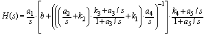 | (1) |
Coefficient values in (1) are readily obtained from running Matlab Toolbox and they are a1=0.5, a2=0.3, a3=0.13, a4=0.39, a5=0.13, k1=1.34, k2=1.2, k3=0.67, k4=0.67, and b1=0.087. The proposed CT ΣΔ modulator circuit is shown in Figure 2. Obviously, the first two stages of the loop filter are active-RC integrators where C1 in series with Rz is to cancel the right-half-plane zero due to the excess loop delay[5]. Passive networks are placed on third and fifth stages of the loop filter. The noises referred to input are therefore suppressed by at least two active integrators. Compared to the prior art, such arrangement can further mitigate the input noise contribution of passive filters.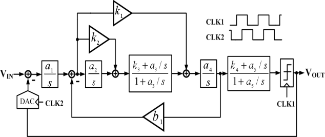 | Figure 1. The architecture of the proposed CT ΣΔ modulator |
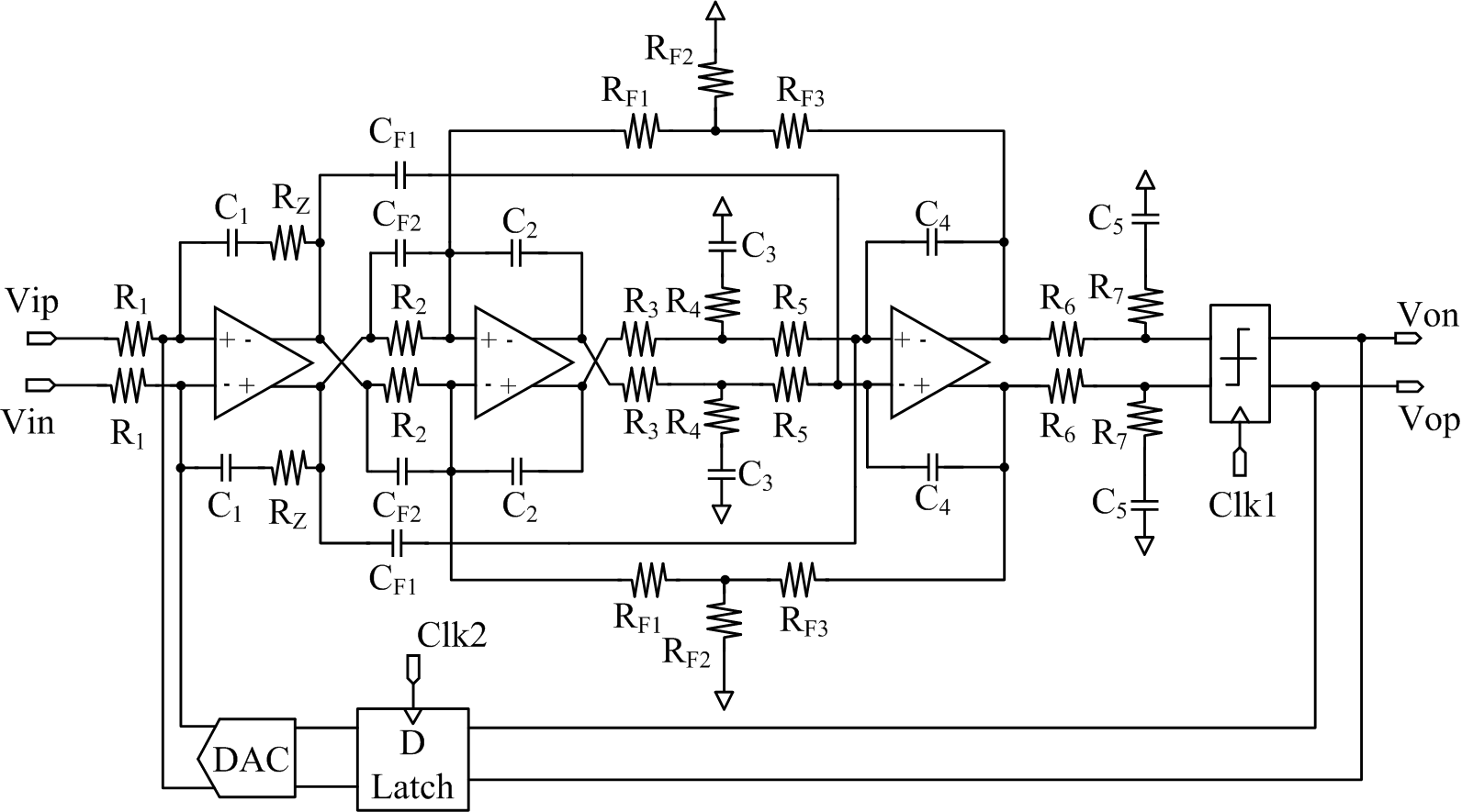 | Figure 2. The proposed CT ΣΔ modulator with a hybrid active-passive loop filter |
2.2. Passive Filter Circuit
The schematic of the passive filter is shown in Figure 3, and the corresponding transfer function is expressed as: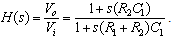 | (2) |
The passive filter is a lossy device with one pole at  and one zero at
  . Since the DC gain is always less than one, the output noise of the passive filter can be directly referred to the input.
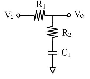 | Figure 3. A passive filter circuit |
2.3. Active Bridge-T Network
Considering the design of the hybrid loop filter, an optimization theory for the passive loop filter based on the trade-off of both circuit noise and noise transfer function is discussed in[3]. However, no optimization theory about poles and zeros of the hybrid loop filter is found. Therefore, the active 3rd order loop filter is first designed with Delta-Sigma Toolbox. The design of poles and zeros of the two passive filters is based on the locations of poles and zeros of the 3rd-order active filter. After embedding the two 1st-order passive filters into the active 3rd-order filter, the dynamic range scaling methodology of the 5th-order hybrid loop filter is performed to ensure op amps are not saturated due to the larger signal swing. This is verified by scaling (increasing or decreasing) the coefficient values of the hybrid loop filter while maintaining its transfer function as identical as possible.The order design of the hybrid loop filter is based on following principles. First, cascading several stages of passive filters should be avoided because of loading effect, attenuation and noise accumulation. Secondly, the active integrators should be preceded passive filters wherever possible since the gain of passive filter is less than one. Although the noise of passive filters can be mitigated with parallel larger capacitance and series smaller resistance, it demands preceded stage with higher driving capability, and hence more power dissipation and consume much chip area due to large capacitance. The local feedback inside loop filters can increase modulator SNDR, but this structure will require more chip area and will cause more cost. The bridge-T network shown in Figure 4 can effectively mitigate this issue.The transfer function of the bridge-T network is: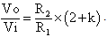 | (3) |
 | Figure 4. An active bridge-T network |
The bridge-T network achieves an effective feedback resistor of R2(k+2). If the feedback resistor R2 is 40 k and k is set to be approximate 5.5, then the equivalent resistance becomes 300 kΩ. This result highly reduces the chip area of feedback resistors by a factor of three times.The fifth order ΣΔ modulator is stabilized by the resistive feedforward {R4/(R3+R4), R7/(R6+R7)}, and the capacitive feedforward (CF2/C2, CF1/C4). The former structure is that in the higher frequency, C3 and C5 are short so that the feedforward paths are formed[3]. Capacitive feedforward is a simple solution compared to conventional CIFF topology[6]. Instead summing all feedforward paths by an extra summation amplifier, which usually demands high slew rate, two capacitive feedforward paths are disturbed by two op amps inside the loop filter.
2.4. Tunable Capacitor Array
Since the resistance variation of R due to the process actually is evident, sometimes the error may highly reach about  . To compensate this large RC product variation, capacitors are implemented as capacitor arrays as shown in Figure 5. The nominal value of the capacitor array is equal to 5C, as (b2, b1, b0)=(0, 1, 0). The capacitor array is tunable from 3C to 10C, corresponding 60% to 200% of the nominal value. The reset switch protects the device returning the modulator to a safe state in case of overload.
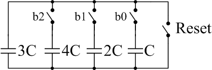 | Figure 5. A tunable capacitor array |
2.5. Operational Amplifier Design
The load capacitance of each amplifier is similar due to deliberate design. The two-stage amplifier is used, shown in Figure 6 which is a two-stage that consists of a differential input stage, a common source output stage with a frequency compensation circuit of Cc in series of R1 and a common-mode feedback (CMFB). The CMFB circuit has advantages of allowing rail-to-rail output swing. Furthermore, it does not need any level shift or attenuation on the common mode signal, unlike other CMFB circuits that use differential pairs. The required gain and bandwidth of the amplifier are determined by simulation. Simulated results illustrate that the op amp achieves a unity gain bandwidth (GBW) more than 350 MHz parallel with a load capacitance of 3 pF and a phase margin of 64°. The low-frequency gain of the op amp is higher than 50 dB at 1.8 V supply voltage. All other performances are summarized in Table 1.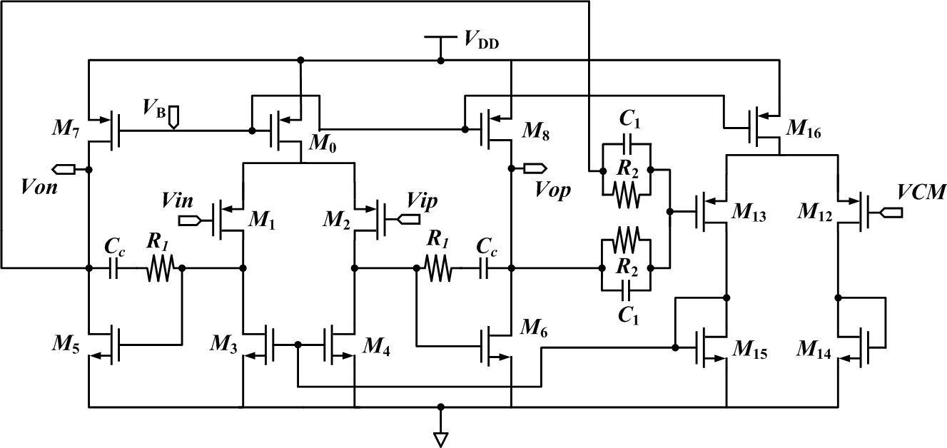 | Figure 6. A two-stage amplifier with commom mode feedback circuit |
| Table 1. Op Amp Performance Summary with an Output Load of 3 pF//25 k |
| | Parameters | Spec. | Pre-Sim. | Post-Sim. | | Output Load | - | 3 pF // 25 k | | DC Gain | > 50 dB | 58.76 dB | 58.8 dB | | Phase Margin | > 60° | 67.9° | 64.3° | | Unity Gain Bandwidth | >350 MHz | 430 MHz | 422 MHz | | Offset Voltage | - | - | 0.1 mV | | Setting Time + (1%) | < 3.9 ns | 1.5 ns | 1.6 ns | | Setting Time - (1%) | < 3.9 ns | 0.8 ns | 1 ns | | Slew Rate + | - | 155.4 V/μs | 126.9 V/μs | | Slew Rate – | - | 219.6 V/μs | 159.5 V/μs | | ICMR | - | 0.23V~1 V | 0.24V ~1 V | | OCMR | > 1V | 0.18V~1.48V | 0.19~1.48V | | PSRR + | > 60dB | - | 84 dB | | PSRR- | > 60dB | - | 82.8 dB | | CMRR | > 60dB | - | 78.6 dB | | THD @ 1 Vp-p,1 MHz Input | < 1% | 0.37 % | 0.39 % | | Power Consumption | < 5mW | 2.88 mW | 2.67 mW | | Input-Referred Noise | - | 13.34 uVrms | 16.69 uVrms | | Layout Area | - | - | 163 x 100 μm2 |
|
|
2.6. Bias with a Start-Up Circuit
The bias circuit used for the proposed modulator is shown in Figure 7. The Iout given in (4) is tunable by varying off-chip resistor RB and is independent of the power supply,  is called the process conduction parameter. The bias circuit requires a start-up circuit to avoid Iout=0. When the gate voltage of MB4 and MB5 is zero, MB7 is turned on to initialize the current. After MB5 and MB4 are turned on, MB7 biased by MB3 and MB6 is turned off immediately.
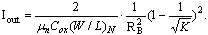 | (4) |
 | Figure 7. The bias with a start-up circuit |
2.7. Quantizer, D-Latch, and Feedback DAC
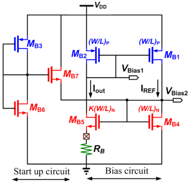
Dynamic comparator circuit with SR (set reset) latch is chosen for low power consumption, as shown in Figure 8. Simulation verifies that the regeneration time is 1.5 ns, the offset voltage is less than 10 mV and the power consumption is less than  . Both the comparator and the D-latch in Figure 8 use the same clock frequency of 128 MHz.
  | Figure 8. Dynamic comparator with SR latch |
But to allocate sufficient regeneration time to the comparator, the D-latch has to be delayed for approximately one-fourth clock cycle. This arrangement greatly reduces harmonic distortion. The D-latch circuit is shown in Figure 9.A complementary current steering DAC with nonreturn-to-zero (NRZ) pulse is adopted, as shown in Figure 10. This circuit is less sensitive to clock jitter compared to return-to-zero (RZ) and half return-to-zero (HRZ) implementation.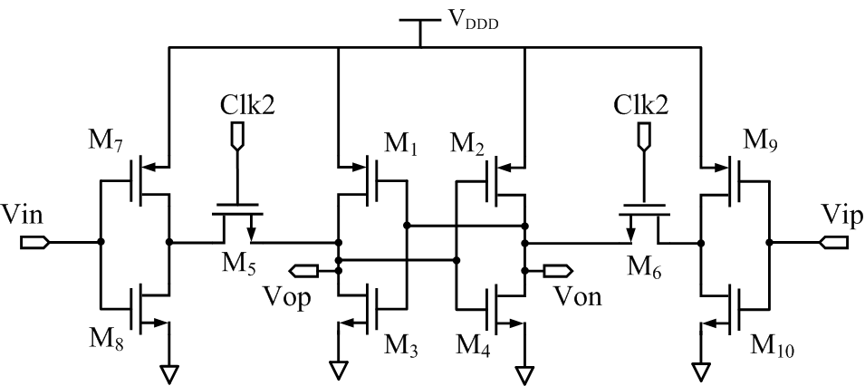 | Figure 9. A D-latch circuit |
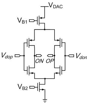 | Figure 10. A DAC circuit |
3. Clock Jitter
Jitter is the undesired deviation often from a reference clock source and may lead to data errors. If there is jitter present on the clock signal to the ADC or DAC then the instantaneous signal error will be introduced. Usually, it is a significant and undesired factor in almost all communications links and can cause loss of transmitted data between ADC or DAC. The amount of tolerable jitter depends on the affected application. A CT ΣΔ modulator is sensitive to the DAC output over the entire feedback period, unlike a discrete-time implementation which relies only on the final settled output value. The DAC timing jitter corrupts the output of the feedback pulse and is often the main error source in high resolution CT ΣΔ modulator[9]. A filter followed can be designed to minimize the effect of sampling jitter. The output of the first feedback DAC is especially critical. CT ΣΔ modulators are also sensitive to clock jitter. In order to quantify the effects of the clock jitter, the modulator was simulated with a normally distributed jittered clock signal. Figure 11(a) depicts the SNDR of the modulator versus clock jitter.To maintain SNDR large than 60 dB, the RMS value of clock jitter must less than 22 ps at the clock rate of 128 MHz. To reduce the sensitivity of clock jitter for CT ΔΣ modulator, SCR feedback is introduced[10]. It could be employed to the single-bit hybrid ΔΣ modulator coefficient deviation of loop filter of CT ΣΔ modulators and is a common issue due to RC product variation, which is about ±30%. Figure 11(b) depicts the modulator SNDR versus the normalized RC product. Obviously, at normalized RC=1, the SNDR is maximum.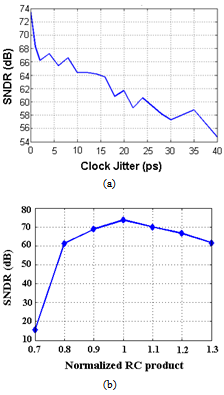 | Figure 11. Simulated SNDR values versus (a) clock jitter and (b) normalized RC product |
4. Measured Results
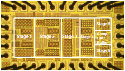 | Figure 12. Chip microphotograph of the proposed ΣΔ modulator with a chip area of 0.642 (1.07x0.6) mm2 |
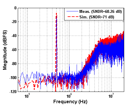 | Figure 13. Output spectrum (input signal: 0 dBm, 500 kHz) |
The proposed prototype chip microphotograph is shown in Figure 12. A balun device in this measurement is selected to convert the single-ended analog signal to a balanced quadrature-differential signal. Notably, op amps often consume the most area. Comparator, DAC and buffer circuits take a small chip. Figure 13 shows the measured output spectrum of the modulator at a sampling rate of 128 MSamples/s. A 0 dBm 500 kHz input sinusoid was used. The measured output stream is loaded into MATLAB and taken 16384 points FFT with Hanning window in order to estimate the SFDR, SNDR, image rejection (IR) and input dynamic range (DR). The measured results of output spectrum accompanying with the simulated results are almost the same shown in Figure 13. The measured peak SNDR is 60.26 dB over a 2 MHz signal bandwidth. Figure 14 shows the measured IM3 to be -48 dB. The SNDR versus input signal level is plotted in Figure 15, showing that the measured dynamic range is 62 dB. Comparison to other reported ΣΔ modulators can be carried out by evaluating the figure-of-merit (FOM)[9]: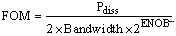 | (5) |
where Pdiss is the power consumption in mW and the bandwidth is in Hz.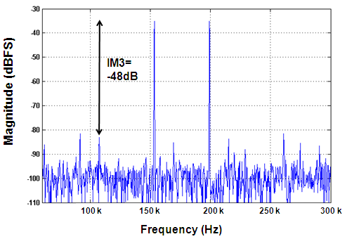 | Figure 14. Two tone test (input signals:153 kHz, 199 kHz with 0.144 Vp-p) |
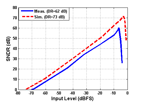 | Figure 15. SNDR with varying input level |
The power consumption is dominated by the amplifiers. At 1.8 V supply voltage, the measured power dissipation is less than 9 mW of which over 88% is dissipated in the op amps and their bias circuitry and about 12% is dissipated in the remaining circuits including D-latch 8.7%, ADC 3.1% and comparator 0.2%. Figure 16 illustrates the reported dissipation matched the expected value based on the simulation and analysis. Figure 17 shows a comparison to the state of the art design FOM. | Table 2. Comparison with Previously Published Papers |
| | | Thiswork | [7] | [8] | [9] | [10] | [11] | [12] | [13] | | Process (μm) | 0.18 | 0.18 | 0.18 | 0.18 | 0.18 | 0.18 | 0.18 | 0.18 | | SupplyVoltage (V) | 1.8 | 1.8 | 1.8 | 1.8 | 1.2 | 1.8 | 1.8 | 1.8 | | Clock Rate (MHz) | 128 | 100 | 2.56 | 100 | 240 | 360 | 800 | 100 | | Bandwidth (MHz) | 2.0 | 3 | 0.02 | 1 | 7.5 | 18 | 10 | 2 | | Peak SNDR(dB) | 60.26 | 57.8 | 65.3 | 56.8 | 67 | 62.5 | 68.4 | 67.7 | | ENOB (bit) | 9.72 | 9.31 | 10.55 | 9.14 | 10.84 | 10.1 | 11.07 | 10.9 | | DR (dB) | 62 | 58 | 71 | 60 | 77 | 68 | 70 | - | | Power (mW) | 9 | 11.8 | 0.42 | 22.2 | 89 | 183 | 160 | 68 | | Chip Area (mm2) | 0.64 | 1.67 | 0.21 | 1.62 | 1.4 | 0.68 | 2.5 | 3.2 | | FOM(pJ/step) | 2.67 | 3.1 | 3.63 | 19.6 | 3.24 | 4.63 | 3.72 | 8.9 |
|
|
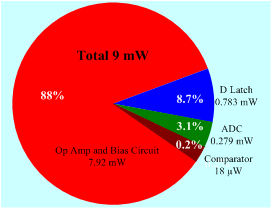 | Figure 16. Pie chart distribution of area and power consumption |
The FOM of (5) is given over the achieved bandwidth of recently reported ΣΔ modulators. This work achieves the lowest power consumption of 9 mW and the best FOM of 2.67 pJ/conv while attaining highly comparable performances in signal bandwidth, peak SNDR and ENOB.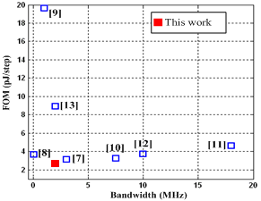 | Figure 17. Comparison to the state of the art design FOM. |
5. Conclusions
A low power CT ΣΔ modulator with a hybrid loop filter is implemented in a TSMC 0.18 um technology. To erase the summation amplifier, the capacitive feedforward structure is employed. To reduce layout area, local feedback resistors are designed to form an active bridge-T network. The proposed hybrid CT ΣΔ modulator establishes better performance compared with other active counterparts. Measured results achieve the best FOM of 2.67 pJ/conv, an ENOB of 9.72-bit and a SNDR of 60.26 dB over a signal bandwidth of 2 MHz while consuming 9 mW from a 1.8 V supply voltage. The overall chip area is only 0.642 mm2. Compared with active ΣΔ modulators, the proposed ΣΔ modulator features less hardware complexity because the hybrid loop filter includes two passive filters, which are very simple to implement.
ACKNOWLEDGEMENTS
The authors would like to thank the staff of the CIC for the technical supports.
References
| [1] | F. Chen, S. Ramaswamy, and B. Bakkaloglu, “A 1.5V 1mA 80dB passive ΣΔ ADC in 0.13μm digital CMOS process,” ISSCC Dig. Tech. Papers, 2003, pp. 496–497. |
| [2] | T. Song, Z. Cao, and S. Yan, "A 2.7-mW 2-MHz continuous-time delta sigma modulator with a hybrid active-passive loop filter," IEEE J. Solid-State Circuits, vol. 43, no. 2, pp. 330-341, Feb. 2008. |
| [3] | R. Zanbaghi and T.S. Fiez, “A novel low power hybrid loop filter for continuous-tme sigma-delta modulators.” In Proc. of IEEE ISCAS, pp. 3114-3117, May 2009. |
| [4] | J. F. Huang, Y. J. Lin, K. C. Huang and R. Y. Liu, “A CT Sigma-Delta modulator with a hybrid loop filter and capacitive feedforward,” The 54th IEEE International Midwest Symposium on Circuits and Systems, pp.1-4, Aug. 2011. |
| [5] | L. J. Breems, E. J. van der Zwan, and J. H. Huijsing, “A 1.8-mW CMOS modulator with integrated mixer for A/D conversion of IF signals,” IEEE J. Solid-State Circuits, vol. 35, pp. 468–475, Apr. 2000. |
| [6] | L. Dorrer et al., “A 3mW 74-dB SNR 2-MHz continuous-time delta-sigma ADC with a tracking ADC quantizer in 0.3-μm CMOS,” IEEE J. Solid-State Circuits, vol. 40, no. 12, pp. 2416-2427, Dec. 2005. |
| [7] | S. W. Huang, Z. Y. Chen, C. C. Hung, and C. M. Chen, “A fourth-order feedForward continuous-time delta-sigma ADC with 3MHz bandwidth,” In Proc. of IEEE MWSCAS, pp. 33-36, Aug. 2010. |
| [8] | M. C. Huang and S. I. Lu, “A fully differential comparator-based switched-capacitor ΔΣ modulator,” IEEE Trans. Circuits Syst. II, vol. 56, pp. 369–373, May 2009. |
| [9] | J. A. Cherry and W. M. Snelgrove, “Clock jitter and quantizer metastability in continuous-time delta–sigma modulators,” IEEE Trans. Circuits Syst. II, vol. 46, no. 9, pp. 661-676, June. 1999. |
| [10] | S. D. Kulchycki, R. Trofin, K. Vleugels, and B. A. Wooley, “A 77-dB dynamic range, 7.5-MHz hybridcontinuous-time/discrete-time cascaded ΣΔ modulator,” IEEE J. Solid-State Circuits, vol. 43, no.4, pp. 796-804, Apr. 2008. |
| [11] | Y. S. Shu, J.Kamiishi, K. Tomioka, K. Hamashita, and B. S. Song, “LMS-based noise leakage calibration of cascaded continuous-time ΣΔ modulators,” IEEE J. Solid-State Circuits, vol. 45, no. 2, pp. 368-379, Feb. 2010. |
| [12] | C. Y. Lu, J. F. Silva-Rivas, P. Kode, J. Silva-Martinez, and S. Hoyos, “A sixth-order 200 MHz IF bandpass sigma-delta modulator with over 68 dB SNDR in 10 MHz bandwidth,” IEEE J. Solid-State Circuits, vol. 45, no. 6, pp. 1122-1136, June 2010. |
| [13] | J. Choi, K. Jang, J. Lee, W. Jeong, J. Park, J. Yoon, S. Lee, and J. Choi, “Design of wide-bandwidth sigma-delta modulator for wireless transceivers,” in Proc. IEEE Int. Symposium on Integrated Circuits, pp. 598-601, Singapore, 2009. |
 Abstract
 Reference
 Full-Text PDF
 Full-Text HTML