-
Paper Information
- Previous Paper
- Paper Submission
-
Journal Information
- About This Journal
- Editorial Board
- Current Issue
- Archive
- Author Guidelines
- Contact Us
Microelectronics and Solid State Electronics
2012; 1(2): 47-52
doi: 10.5923/j.msse.20120102.05
Ultra-Low-Power Ultra-Fast Hybrid CNEMS-CMOS FPGA
 Abstract
 Reference
 Full-Text PDF
 Full-Text HTML
Vijay K Sirigir1, Sijing Han1, Daniel G. Saab1, Khawla Alzoubi2, Massood Tabib-Azar3
1Case Western Reserve University, Cleveland, OH 44106 USA
2Khawla Alzoubi is with Tafila Technical University, Tafila, Jordan
3University of Utah, Salt Lake City, UT 84112 USA
Correspondence to: Sijing Han, Case Western Reserve University, Cleveland, OH 44106 USA.
| Email: |  |
Copyright © 2012 Scientific & Academic Publishing. All Rights Reserved.
Static power consumption has become a major concern in the design. To address this, we have designed a novel Nano-Electro-Mechanical (NEM) switch with virtually zero leakage current, 1 to 2 Volts operation voltage, 1 ns switching time, > 1 GHz fundamental resonant frequency, and nanometer-scale footprint. Positive and negative channel switches from Complementary NEMS (CNEMS), similar to CMOS. Due to compatibility between CNEMS and CMOS, these CNEMS switches can be hybridized with CMOS at the metallization or device. In this paper, we present the CNEMS design, its electrical properties and a hybrid FPGA with CNEM switches. We used VPR to simulate the MCNC benchmark circuits routed on our hybrid FPGA for power and delay. Our experimental results show an average 98%, 85%, 71% and 99.99% reduction in critical path delay, routing energy, total energy, leakage power when comparisons are made with FPGA design using pure CMOS technology (180 nm technology and hybrid CNEMS and 180 nm CMOS).
Keywords: FPGA, HYBRID CNEM-CMOS, NEMS
Article Outline
1. Introduction
- CMOS integrated circuit technology provided a continuous improvement in integration level, cost and performance over the last four decades. This has lead to tremendous development in computation, data storage and information processing. Energy and power dissipation for the sub- nanometer CMOS increased drastically due to short channel effect, sub-threshold leakage, hot carriers injection, intra-die, inter-die process and thermal variations. Energy and power are more important for FPGA designs which are constrained by higher power consumption when compared to Application Specific Integrated Circuits (ASIC). This limits the use of FPGA. It was observed that in FPGA, programmable interconnection[9], and resources consume significant energy at the cost of offering flexibility[8] to the design.Significant amount of research work has been attributed to designing energy efficient FPGA architecture and routing efficient algorithms. In[6, 10], they realized power efficient FPGA by assigning programmable low VDD (0.9V) to non timing critical CLB’s and high VDD (1.1V) to the timing critical CLB. They reported an average power saving of 61% at the cost of increased area. The increased area is due to the use of additional level converters and routing multiplexers.In[13], they proposed a new FPGA routing switch that can be programmed to operate in three modes: high-speed, low-power or sleep-mode. In the sleep mode, applied to unused switches, offers significant leakage reductions. In the sleep-mode the leakage power is reduced by 36%-40% over the high speed mode, and the dynamic power is reduced by up to 28%.[14] Proposed reducing FPGA power by the use of Dual threshold CMOS (DTCMOS) based switches instead of NMOS. The area overhead is kept to minimum. The sleep transistor is used to reduce the sub-threshold voltage. They reduce the power-delay product by 16% and by of 20% in active and standby mode, respectively.In[16], The NEMS switch[18] is proposed to be used in NEMS-CMOS hybrid LUT, and it is compare to CMOS LUT in terms of power and delay. The simulation results show that the delay is almost the same, but the power is reduced by 90% in the NEMS-CMOS LUT over CMOS LUT.In[17], CMOS-Nanorelay FPGA (cFPGA) was developed using new two CMOS transistors and one NEMS relay. They proposed using vertical carbon Nanotube which is relatively easier than horizontal carbon Nanotube to fabricate. This results in reducing dynamic power by 30%. Carbon nano-tubes are much harder to make and cannot integrate seamlessly with current CMOS technology.In this paper, we introduce a configurable Complimentary Nano-Electro-Mechanical Switch (CNEMS) metallicswitching device as a replacement of CMOS devices in the switch and connection block components found in FPGA architectures. The new metallic CNEMS switch uses the same CMOS fabrication steps and materials. This makes it easy for the CNEMS switch to be ”dropped” in and hybridized, seamlessly, with CMOS at the metallization or at the device level to manage leakage current and power consumption. The CNEMS with its innovative structure operates at 1GHZ resonating speed, has a low turn on voltage between 1 to 2 volts, near zero current leakage, and near zero parasitic capacitance. The CNEMS switch significantly reduces the power consumption, increases the FPGA speed and offers seamless integration with CMOS technologies.The rest of this paper is organized as follows: Section 2 describes the CNEMS device structure. Section 3 presents the 3D FEA physical device model, illustrates extraction of mechanical and electrical properties and explains CNEMS digital logic gates. Section 4 explores the approach and presents experimental setup and results. Conclusions are presented in section 5.
2. Device Design
- Figure 1 shows structure of a four terminal NEM switch. The switch has a moveable cantilever beam with nickel coated on an oxide layer. In initial position, the direct metal-metal contact between drain/source and cantilever form direct current path. With applied voltage Vgb between gate and cantilever, the electric force and the small Van der Waals force attract the cantilever to move towards the gate. During the attraction, a gap between the cantilever and the gate decreases. With the voltage reaching a threshold value or pull-in voltage (Vpi), the gap reduces to a critical value, 1/3 of initial gap and then the cantilever abruptly contacts the gate to break the direct current path between drain and source. When the voltage Vgb between the gate and the cantilever decreases to a small value or pull-out voltage (Vpo), the cantilever leaves the gate and contact drain and source to form the direct current path again.
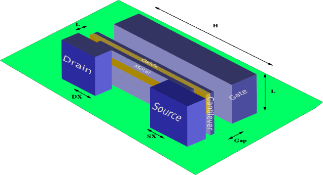 | Figure 1. Schematic of a four terminal switch geometry |
 | Figure 2. (a) Pull-in voltage with Van der Waals force 1.64 V. (b) Pull-in voltage without Van der Waals force 1.95 V |
3. Physical Device Model and CNEMS Digital Design
- A. Physical Device CharacteristicsTo capture multi-physics phenomena of a four terminal switch, a 3D FEA physical device model is constructed using FEA simulation tool (COMSOL multi-physics). This model is capable of capturing the multi-physics of the four terminal NEM switch as well as re-producing its electro-mechanical characteristics.Pull-in voltage: The pull-in voltage is solved by static-parametric solver in COMSOL multi-physics. In the solver, the fringing effect is ignored as a result of the small gap (1.5 nm)[20]. We consider Van der Waals[21] force on the cantilever surface facing to the gate due to the small gap (1.5 nm). The attractive Van der Waals force reduces the pull-in voltage about 0.3 V. The simulated pull-in voltages with Van der Waals force and without Van der Waals force are shown in Figure 2. Note, the simulation stops just before the contact happens.Switching time: The time dependent solver in COMSOL multi-physics is used to solve switching time with applying pull-in voltage between the cantilever and the gate. The simulation result in Figure 3(a) shows the switching time is about 1 ns. The input capacitance is a very important parameter for the switch. The change of the capacitance with time shown in Figure 3(b) is modelled by setting capacitance density on the cantilever surface. The boundary integration function integrates the capacitance between the cantilever and the gate for each time point.
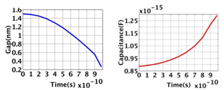 | Figure 3. Switching time versus the gap between the cantilever and the gate and gate capacitance versus the time |
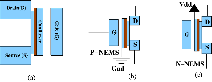 | Figure 4. (a) NEMS device structure; (b) P-NEMS device configuration; (c) N-NEMS device configuration |
 | Figure 5. CNEMS inverter |
4. Power Reduction in CNEMS-CMOS FPGA
- A. FPGA BackgroundFigure 6(a) shows a typical island style 2-D Field Programmable Gate Array (FPGA). This FPGA is composed of an array of Configurable Logic Blocks (CLBs), a programmable interconnection switch box and I/O Pads. The CLBs store the truth tables of functions in Random Access Memory (RAM). The switch box is implemented using CMOS programmable switches as shown in Figure 6(b). In this configuration the CMOS switch current leakage and capacitive/resistive causes the FPGA to consume more power and to operate at a lower clock frequency. In this paper, we introduce a novel Nano-Electro-Mechanical Switch (NEMS) configurable architecture which can be used to replace the CMOS switches in the FPGA switch box (Figure 6(c)). Unlike CMOS switches, the NEMS switch operates with a near zero off-state current leakage and a very low on-state resistance (30 Ω). The reduction in the off-state current leakage and the very low on-state resistive loading allow the FPGA to operate at lower power and faster clock rate. The NEMS switch in this environment is used only during configuration. This use of the NEMS switch overcomes the speed degradation caused by the mechanical movement. The configuration time may increase slightly by it is compensated with the speed and power dissipation reduction during computation cycles. We study island style FPGA architectures for our work and we use the terminology adopted in[15].
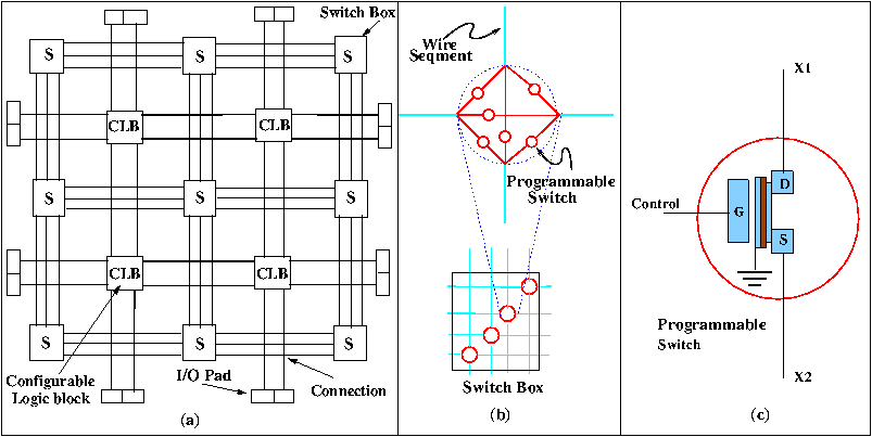 | Figure 6. FPGA architecture; (a) Island-style FPGA consisting of I/O Pads, Configurable Logic Block (CLB), and Switch Blocks for routing; (b) Switch Box architecture design and programmable switches; (c) A Programmable NEMS switch. When Control=0 then X1and X2 are connected and not when Control=1 |
 | Figure 7. Critical path saving, routing energy saving and total energy saving of different MCNC circuits for K=4 and N=4, K=4 and N=8, K=3 and N=10 and K=7 and N=10 settings |
5. Conclusions
- In this paper, we presented a configurable CNEM metallic switching device as a replacement of CMOS devices in the switch and connection block components found in FPGA architectures. The new metallic CNEM switch uses the same CMOS fabrication steps and materials, operates at 1GHZ resonating speed, has a low turn on voltage between 1 and 2 volts, near zero current leakage, and near zero parasitic capacitance. We showed, experimentally, that the CNEM switch significantly reduced the power consumption, increased the FPGA speed and offers seamless integration with CMOS technologies. In our experiment, the CNEM FPGA architecture achieves an average 98%, 85%, 71%, and 99.99% reduction in critical path delay, routing energy, total energy, leakage power over CMOS (180nm) FPGA architecture.