-
Paper Information
- Paper Submission
-
Journal Information
- About This Journal
- Editorial Board
- Current Issue
- Archive
- Author Guidelines
- Contact Us
Microelectronics and Solid State Electronics
p-ISSN: 2324-643X e-ISSN: 2324-6456
2012; 1(2): 33-40
doi:10.5923/j.msse.20120102.03
Reliability and Retention of Floating Body RAM on Bulk FinFET
 Abstract
 Reference
 Full-Text PDF
 Full-text HTML
M. Aoulaiche1, E. Simoen1, Ch. Caillat2, N. Collaert1, G. Groeseneken1, M. Jurczak1
1Imec, Kapeldreef, 75, 3001 Leuven, Belgium
2Micron Technology Belgium, Kapeldreef 75, 3001 Leuven, Belgium
Correspondence to: M. Aoulaiche, Imec, Kapeldreef, 75, 3001 Leuven, Belgium.
| Email: |  |
Copyright © 2012 Scientific & Academic Publishing. All Rights Reserved.
This paper assesses one Transistor Floating Body Random Access Memory (1T-FBRAM) in Bulk FinFET devices as a candidate for conventional DRAM replacement in the future technology nodes. For the cell operation, Bipolar Junction Transistor (BJT) programming is used. Reliability and retention time of the floating body effect are studied on different gate lengths, fin widths and for different programming biases. The degradation mechanisms during cycling are identified. The optimum number of cycles extracted (~109) is still far below the 1016 cycles expected. Long retention times are obtained; however, with the tail bit distribution below the 64ms DRAM specifications. Besides, the generated floating body takes place beneath the drain at the n+/p+ drain/ground-plane junction, which explains the long retention times by the large junctions area. Moreover, the floating body can be obtained only by leaving floating the bulk contact of the bulk FinFET cell, which makes its integration in a DRAM chip challenging. On the other hand, the bulk FinFET device shows a biristor like behaviour but featuring more options by the use of the gate to control the write and read.
Keywords: Bulk Finfet, BJT, Cycling, Endurance, Floating Body, RAM, Retention
Cite this paper: M. Aoulaiche, E. Simoen, Ch. Caillat, N. Collaert, G. Groeseneken, M. Jurczak, Reliability and Retention of Floating Body RAM on Bulk FinFET, Microelectronics and Solid State Electronics , Vol. 1 No. 2, 2012, pp. 33-40. doi: 10.5923/j.msse.20120102.03.
Article Outline
1. Introduction
- One transistor capacitor-less random access memory (1T-RAM) is considered as a candidate to replace the conventional one transistor and one capacitor 1T/1C DRAM, which suffers from the scaling challenges related to the capacitor integration[1,5]. Various device architectures are considered: bulk, Silicon On Insulators (SOI), double gate, surround-gate etc[6-9]. Among these different architectures bulk FinFET is particularly attractive since it is going to be applied to a mass production, is more scalable than planar bulk devices, can be cointegrated with planar bulk devices and avoids the heat dissipation problem, which is present in SOI FinFET devices. Besides, different biasing schemes are proposed. With regard to the state-1 programming method: impact ionization and band-to-band tunnelling are the main mechanisms to create excess holes in the floating body[10]. On the other hand, with regard to the read method, two groups can be noticed: in the first group (Gen1), the floating body charge induces a threshold voltage shift, which changes the MOSFET current. The second group (Gen2), which is proven to improve 1T-DRAM performances and provide fast read and better scalability[4,7] uses the Bipolar Junction Transistor (BJT) present in the MOS structure. To be viable, 1T-DRAM candidate has to satisfy conditions such as: high scalability, low intrinsic variations, high programming speed, high sense margin, long retention time and good endurance. This paper investigates the retention and reliability of 1T-FBRAM on bulk FinFET devices. In section 2, the device fabrication and the experimental conditions are described. In section 3, the operating conditions and biases are depicted. In section 4 and 5 endurance and retention are respectively discussed.
2. Device Fabrication and Experimental Conditions
- The devices are fabricated on bulk Si-substrate with doped ground plane, as illustrated in Fig.1. Fin widths down to 10nm for a fin height of HFIN=60nm were made using 193nm lithography. The gate electrode consists of a 5nm SiO2 capped with 5nm PE-ALD TiN and 100nm poly. After gate patterning, the extensions were implanted and the nitride spacers were formed. No selective epitaxial growth (SEG) was done on the source/drain areas. A NiPt-based salicide process was used after the deep S/D implants which were activated by a spike anneal. Finally, a standard Cu back-end-of-line process was used to finish the devices[6]. The measurements of the Floating Body Random Access Memory (FBRAM) were performed by applying short pulses at the drain and gate terminals, while keeping the bulk contact floating. The source current is measured during the read pulse using a current amplifier. All the devices measured consist of five fins, as shown in Fig.2.
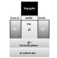 | Figure 1. Lateral view of one fin cut along the channel from the source to drain |
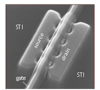 | Figure 2. SEM view of a typical 5 fin bulk FinFET investigated |
3. Operating Conditions
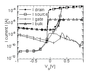
- A double sweep of the ID-VGS characteristic of bulk FinFET devices with the substrate contact grounded or left floating and at high VDS exhibits a large hysteresis, as shown in Fig.3. Moreover, a high current difference between the low and high state is measured. Therefore, this bistable effect is used for the floating body memory programming. During forward sweep, when the gate bias is close to the transistor threshold voltage (Vtf), holes are generated by impact ionization near the drain. These holes are injected into the substrate and raise the body potential, and then the parasitic BJT is turned on. During the VG sweep-back the holes injected by impact ionization keep the BJT current on (state-1) until the positive feedback loop between the impact ionization current and the source-bulk junction forward bias cannot be sustained anymore. Hence, below VG= Vtb the BJT current turns off (state-0)[11].The operating biases used in the dynamic operation and reproducing the floating body effect observed in DC operation are shown in Fig.4.
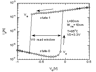 | Figure 3. Double sweep ID-VGS measured on a bulk FinFET with L=80nm, WFin=10nm and at T=85℃, showing the BJT current off (state-0) and on (state-1) |
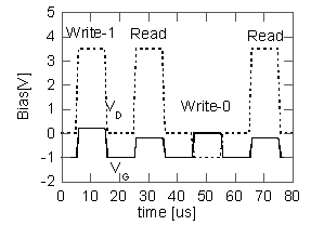 | Figure 4. Schematic of the operating biases applied to the cell during write, read and cycling. The substrate is left floating. |
 | (1) |
 | (2) |
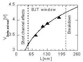 | Figure 5. Gate length dependence, of the VD bias used for the write and read with BJT programming |
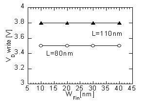 | Figure 6. VD write bias as a function of the fin width and for fixed L=110nm and 80nm |
4. Endurance
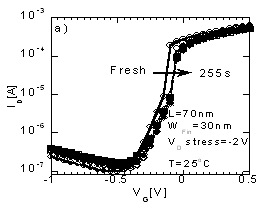
- Since the write-1 and read mechanisms use impact ionization, which is known as a reliability issue[15], endurance and the impact of the gate length and fin widths using the biasing conditions shown in Figs. 5 and 6 are investigated.Degradation mechanismsFig.7 and 8 show the ID-VGS characteristics shifts under a constant voltage stress at (VG=0V, VD=-2V) and at (VG=0V, VD=3.2V) corresponding to the write-0 and write-1 condition, respectively. No significant impact of the stress under the write-0 is observed as a function of the stress time (see Fig.7). However, a small shift towards more positive VG is observed, indicating a negative charge generated by the stress. Conversely, a large shift in ID-VGS characteristics to more negative VG is observed under the stress in the write-1 condition (see Fig.8). This confirms that the dominant degradation is generated during the write-1 condition, where impact ionization is used.
 | Figure 7. ID-VG characteristics measured at different stress times under the write-0 stress condition (VG=0V, VD=-2V) |
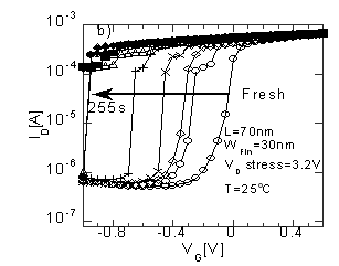 | Figure 8. ID-VG characteristics measured at different stress times under the write-1 stress condition (VG=0V, VD=3.2V) |
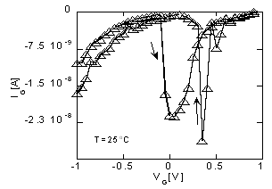 | Figure 9. Gate current measured as a function of VG during the hysteresis measurement as shown in Fig.3, showing hole tunnelling to the gate |
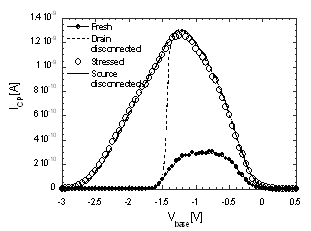 | Figure 10. Base level sweep charge pumping current measured before and after stress under high drain bias of a device with 65nm height, WFin=0.25μm and L= 1μm at 25℃ |
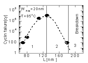 | Figure 11. Cycling failure extracted at 50% ΔIS shift and for different gate lengths. 1 cycle corresponds to the scheme in Fig.4 |
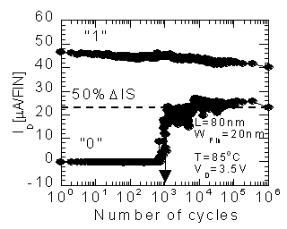 | Figure 12. State-1 and 0 shifts as a function of the number of cycles, showing the state-0 degradation |
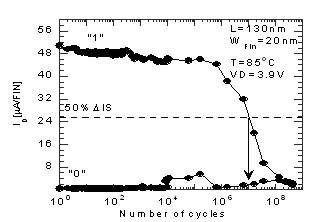 | Figure 13. State-1 and 0 shifts as a function of the number of cycles, showing the state-1 degradation |
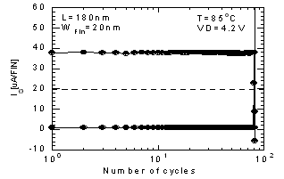 | Figure 14. State-1 and 0 measured as a function of the number of cycles, showing the state-0 and 1 failure |
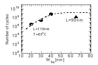 | Figure 15. Cycling failure extracted a 50% ΔIS shift as a function of the fin width |
5. Retention
- The retention distribution of 30 devices measured over the wafer is shown in Fig.16. High retention times are observed. However, the distribution is over ~5 decades of time, from 0.2ms to 10s.
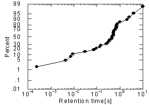 | Figure 16. Retention time distribution measured on 5 fin bulk FinFET devices with L=80nm and WFin=30nm at 85℃ |
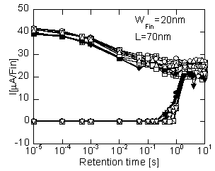
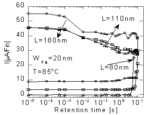 | Figure 17. Retention time measured on bulk FinFET devices with fixed WFin=20nm and different gate lengths at 85℃ |
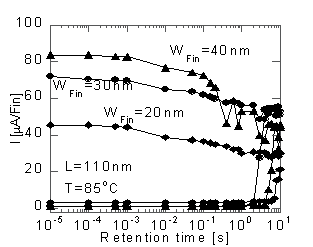 | Figure 18. Retention time measured on bulk FinFET devices with fixed L=110nm and different fin Widths at 85℃ |
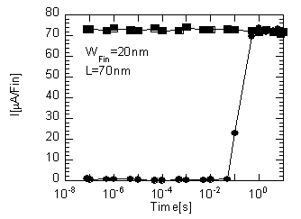
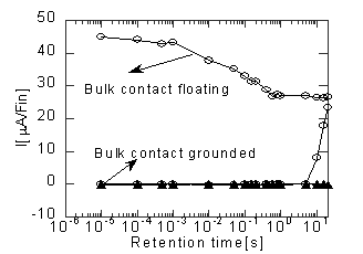 | Figure 19. Floating body retention time measured with the bulk contact floating and grounded on a bulk FinFET device with WFin=20nm, L =80nm and at 85℃ |
 | Figure 20. DC hysteresis measured on a bulk FinFET device with WFin=20nm, L=110nm, at VD=3.5V and at T=25℃ |
 | Figure 21. Retention time measured for VG hold varying from -2V to +2V, showing no effect on the stored holes |
 | Figure 22. Retention time measured on a bulk FinFET with the gate and bulk contact left floating |
6. Conclusions
- The floating body effect in bulk FinFET devices is investigated for 1T-DRAM application, using the BJT programming mode. High memory window and sense margin are observed as expected from the BJT programming. However, during cycling the sense margin is degraded due to interface defects generation and positively charged traps close to the drain, where hot holes are generated during the write condition of the state-1. The cycling failure is observed depending on the fin length and width. Nevertheless, the optimum number of cycles (~109) remains below the 1016 expected by conventional DRAM specifications. Besides, long retention times (~10s) can be obtained. However, the tail bit distribution is below the 64ms DRAM requirement. It is also shown that the floating body effect is due to holes stored in the ground-plane below the drain junction and not in the fin volume of the bulk FinFET. Therefore, the floating body effect disappears for grounded bulk FinFET cells what enhances the challenge of 1T-FBRAM chip fabrication. Furthermore, similar behavior of the floating body as in a biristor is observed when leaving the gate and bulk contacts of the bulk FinFET device floating.
ACKNOWLEDGMENTS
- This work is supported by imec’s partners and core partners on the emerging memory research program: Intel, Micron, Panasonic, Samsung, TSMC, ELPIDA, Hynix, Sony, and FUJITSU.