Messaadi Lotfi, Dibi Zohir
Department of Electronics, Advanced Electronic Laboratory (LEA), University of Batna Street Chahid Mohamed Boukhlouf 0500, Batna Algeria
Correspondence to: Messaadi Lotfi, Department of Electronics, Advanced Electronic Laboratory (LEA), University of Batna Street Chahid Mohamed Boukhlouf 0500, Batna Algeria.
| Email: |  |
Copyright © 2012 Scientific & Academic Publishing. All Rights Reserved.
Abstract
An empirical self-heating SPICE MOSFET model which accurately portrays the vertical DMOS power MOSFET electrical and thermal responses is presented. This macro-model implementation is the culmination of years of evolution in MOSFET modeling. This new version brings together the thermal and the electrical models of a VDMOS MOSFET. The existing electrical model[2,3] is highly accurate and is recognized in the industry. The sequence of the model calibration procedure using parametric data is described. Simulation response of the new self-heating MOSFET model track the dynamic thermal response and is independent of SPICE’s global temperature definition.
Keywords:
Device Characterization, Device Modeling, High Power Discrete Devices, Modeling, MOS Device, Power Semiconductor Devices, Semiconductor Devices, Simulation, Thermal Design, Spice
1. Introduction
Many power MOSFET models available today are based on an ideal lateral MOSFET device. They offer poor correlation between simulated and actual circuit performance in several areas. They have low and high current inaccuracies that could mislead power circuit designers. This situation is further complicated by the dynamic performance of the models. The ideal low power SPICE level-1 NMOS MOSFET model does not account for the nonlinear capacitive characteristics Ciss, Coss, Crss of a power MOSFET. Higher level SPICE MOSFET models may be used to implement the non-linear capacitance with mixed results. The need for this higher level modeling accuracy becomes apparent in high frequency applications where gate charge losses as a proportion of overall losses become significant. The inherent inaccuracies of modeling a power VDMOS with the SPICE MOSFET model dictated need for an alternative approach; a macro-model. A macro-model such as the one defined by Wheatley and Hepp[1] can address the short comings of the ideal low power SPICE MOSFET model. Highly accurate results are possible by surrounding a temperature independent gain block (implemented using three level-1 MOSFET models) with resistive, capacitive, inductive and other SPICE circuit elements.It is possible to develop a model from parametric measurements in a single iteration. The model extraction procedure from parametric data must follow a given sequence. Many of the changes to the model affect different behavior. Failure to follow this sequence will result in repeated model calibration iterations. The MOSFET model reference on which this work is based has been explained in[1-3,10]. The reader is encouraged to refer to these references for a full understanding of the MOSFET model parameters herein referenced. Use of the model, once extracted is not discussed here, but reference[10] addresses the use. Recent works[8,9] have demonstrated methods of circumventing the SPICE global temperature definition, providing a means of using the device’s own junction temperature as a self-heating feedback mechanism.The model developed in[8] has limitations involving proprietary algorithms, rendering the method of limited interest. Model implementation is convoluted, involving a MOSFET analog behavioral model (ABM) implementation whose operating characteristics are dependent on a SPICE level-3 NMOS MOSFET. As a result, both the switching circuit and the load must be duplicated for the model to function. The implementation in[9] does not model the drain-source avalanche property of a MOSFET. Neither[8] nor[9] attempt to model the temperature characteristics of the intrinsic body diode. Introduced self-heating modeling concepts are non-proprietary and may be adapted to other MOSFET models.
2. DMOS Model
A basic model for DMOS transistors has been in use for well over 10 years. The model is based on a vertical structure implemented using an N- epitaxial layer on an N+ doped substrate. The graphics in Figure 1 depict the construction of a unit DMOS cell as well as a cross section showing the various elements of the model. The elements are then arranged for simplicity into the schematic representation of Figure 2.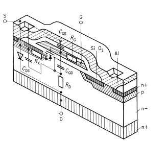 | Figure 1. Structure of a power MOSFET (DMOS) with the parasitic elements important for the component behavior |
Although this model has been in wide use, its implementation and parameterization have left much to be desired especially in SPICE. A great improvement has been made possible by the extensions now available in SPICE, especially the analog behavior models ABM.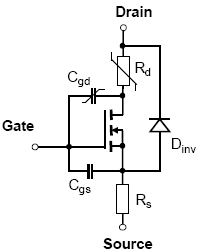 | Figure 2. The circuit diagram of a DMOS model shows the principals and reflects the structural elements of figure 6 |
3. Modeling of Temperature Dependent Component Parameters
The temperature dependence of semiconductor device parameters is often regarded as a second order effect and often dealt with based on rules of thumb or experience.This is not possible in the case of power semiconductors, as the power generated within the device significantly effects its characteristics. The temperature dependent parameters having the most significant impact are mobility (both bulk and surface values) and threshold voltage. These appear in the channel model for MOS transistors and are well defined. This presents a problem in that most models do not include a temperature node (the solution to this will be discussed later when the specific simulation programs are addressed).In order to be able to simulate the inherent heating dynamically, an interactive coupling of the thermal description with the MOSFET model is necessary as shown schematically in figure 8. For this, the instantaneous power dissipation in the transistor (Id x Uds) is determined at all times and a current proportional to the dissipated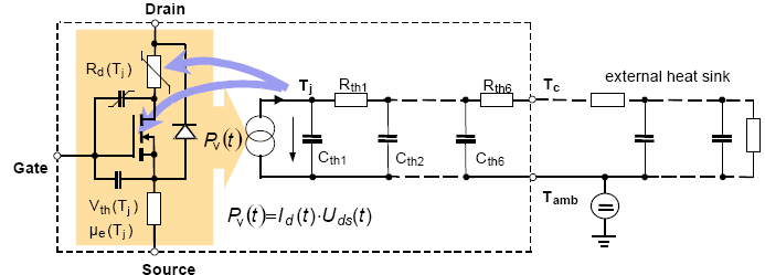 | Figure 3. Principle circuit diagram of a model with interactive coupling of electrical and thermal component description |
4. Self-Heating Spice MOS Model
The self-heating macro-model from Figure 4 is the evolution of years of work and improvements from numerous authors[1-7]. Knowledge of device physics or process details is not necessary to implement the parametric data within the model.Parametric data for several temperature points are used for model calibration resulting in a macro-model which provides representative simulation data for any rated operating junction temperature Temperature dependent model parameters respond in closed loop form to the junction temperature information provided by node Tj. Performance is independent of SPICE’s global temperature definition listed as .TEMP and temperature option TNOM, circumventing the level-1 NMOS model primitive temperature limitation. All MOSFET operating losses are inclusive in the current source G_Pdiss representing instantaneous power dissipation into the thermal model.Multiple MOSFETs may be simulated at different and variable junction temperatures. Each MOSFET may be connected to a heat sink model via node Tcase. The heat sink model may be device specific, so heat sink optimization becomes possible. Current source G_Pdiss is referenced to the simulation ground reference, permitting use of the model in bridge topologies.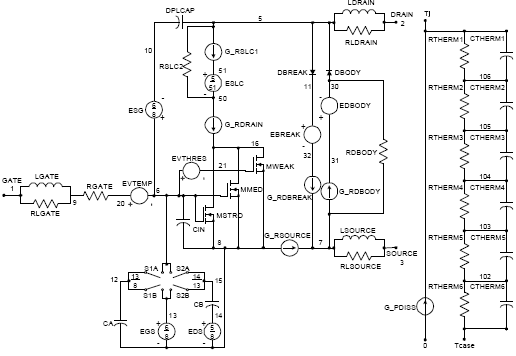 | Figure 4. Self-heating MOSFET macro-model independent of global temperature definition |
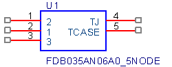 | Figure 5. Self-heating MOSFET symbol |
An example of a symbol representation of the self-heating MOSFET model is shown in Figure 5. Recommended symbol implementation is to designate the pin out attribute for Tj as optional (ERC = DON’T CARE, Float=Unique Net). Tj is the representation of the device junction temperature. It may be used as a monitoring point, or it may be connected to a defined voltage source to override the self-heating feature. Tcase must be connected to a heat sink model. Treatment of connections to the model’s gate, drain, and source terminals are no different than those of the standard MOSFET model.
5. Electro Thermal Spice MOS Model
Ability to describe the value of a resistor and its temperature coefficients as a behavioural model referenced to a voltage node is necessary to express dependence on junction temperature. PSPICE resistor ABMs do not permit voltage node references. Dynamic temperature dependence of the MOSFET’s resistive element (expressed as separate lumped elements) and of the diode’s resistive component cannot be implemented without a resistor ABM. This limitation is overcome with a voltage-controlled current source ABM expression (Figure 3). By using the nodes of the current source for voltage control, resistor behaviour may be expressed as I= V/R(Tj). The resistance R(Tj) is replaced by a behavioural model expression dependent on the voltage node Tj representation of junction temperature. This voltage-controlled current source ABM model was used to implement voltage dependent expressions of RDRAIN, RSOURCE, and RSLC1. Temperature dependent resistive elements of diodes DBODY and DBREAK were separated from the diode model, and expressed as voltage-controlled current source ABM models G_RDBODY and G_RDBREAK. A very large value resistor RDBODY was added to improve convergence. EDBODY is added in series with DBODY to incorporate the temperature dependency of the intrinsic body diode forward conduction drop. Junction temperature information is implemented by the inclusion of the MOSFET’s thermal network ZθJC and current source G_PDISS. The thermal network parameters are supplied in Fairchild Semiconductor data sheets. G_PDISS calculates the MOSFET instantaneous operating loss, and expresses the result in the form of a current. This is a circuit form implementation of the junction temperature from expression (1)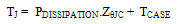 | (1) |
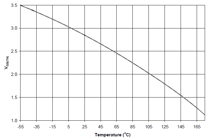 | Figure 6. Experimental data threshold voltage characteristics VGS (TH) (ID=250uA) |
Where TJ = junction temperature, Pdissipation = instantaneous power loss, ZθJC = thermal impedance junction- to-case and Tcase = case temperature. The unit conversion for the electrical analogy of the thermal system is listed in Table 1.| Table 1. Electrical/thermal analogy |
| | Electrical | Thermal | | Ohm | ℃/Watt | | Farad | Joules/℃ | | Amp | Watt | | Volt | ℃ |
|
|
6. Parameter Extraction Methodology
The sequence of the parameter extraction procedure is very important since many of the changes to the library affect different behaviour. For instance, changing parameters in the transfer curve affect the saturation curves. The recommended methodology is shown below.6.1 The transfer curve6.2 The saturation curve6.3 The body diode forward conduction6.4 Breakdown voltage6.5 Trr6.6 Capacitance (Crss, Coss, Ciss)6.7 Gate charge6.8 Temperature coefficients6.9 Thermal modelExtraction is achieved more rapidly if data is plotted log-log, semilog, versus t, etc. First extraction may take days. It becomes a rapidly learned process with repeated usage.
6.1. Transfer Curve
Three level-1 MOSFET transistors are used to model the gain block for the full current range from the sub-threshold region through high current. The three transistor models are MweakMOD, MmedMOD and MstroMOD. The parameters VTO and KP of each transistor are used for alignment of the model with measured data.MODEL MmedMOD NMOS (VTO=3.3 KP=9 IS=1e-30 N=10 TOX=1 L=1u W=1u RG=1.36 T_ABS=25)MODEL MstroMOD NMOS (VTO=4.0 KP=275 IS=1e-30 N=10 TOX=1 L=1u W=1u T_ABS=25)MODEL MweakMOD NMOS (VTO=2.72 KP=0.03 IS=1e-30 N=10 TOX=1 L=1u W=1u RG=13.6 RS=0.1 T_ABS=25)Source resistance (G_Rsource) is added to lower the gain at high currents. It is also a contributing element to the device RDS(ON).Plotting the square root of IDS versus VGS results in a linear curve instead of a quadratic curve, thus improving the visual resolution of the data at the higher current range.G_Rsource 8 7 VALUE= {V (8, 7)/ (2.5e-3*(1+5e-3*(V (th+)-25)+1e-6*pwr((V(th+)-,+25),2)))}
6.2. Saturation Curves
Several gate biases should be used to model the saturation curves. For instance, to model a standard gate device use VGS = 10V, 5V and 3.5V. G_Rdrain is used to fit the model in the linear region. Increasing G_Rdrain will decrease the current of the saturation curves. Next, the space charge limiting effect is modeled using ESLC. The multiplier X in ESLC (1e-6*X, the exponent of the power statement) is adjusted. Lowering X will round off the curves at high currents. If two saturation curves (for instance at Vgs=10V and Vgs=5V) do not match in the linear region, it may be necessary to readjust KP of the strong transistor MstroMOD. Modeling between transfer and saturation curves will then need to be repeated until both curves fit the data.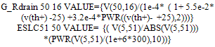
6.3. Body Diode Forward Voltage
Match diode curve data at low currents by adjusting parameters IS and N in DbodyMOD. With the forward voltage plotted on a log scale, N will adjust the slope and IS will shift the curve left or right.MODEL Dbody MOD D (IS=2.4e-11 N=1.04 CJO= 4.35e-9 M=0.54 TT=1.0e-9 XTI=3.9 T_ABS=25)The high current region is modeled on the linear scale. G_ Rdbody is used to match diode curve data at high currents by adding series resistance, thus lowering the curve.G_ Rdbody 7 31 VALUE= {V (7,31) /(1.65e- 3* ( 1+2.7e-3*(V(TH+)-25)+2e- +7*PWR((V(TH+)-25),2)))}IKF can be used to smooth the transition region between low currents and high currents. After changing IKF, it is often necessary to readjust G_ Rdbody.MODEL DbodyMOD D (IS=2.4e-11 N=1.04 CJO= 4.35e- 9 M=0.54 TT=1.0e-9 XTI=3.9 IKF=100 T_ABS=25)
6.4. Breakdown Voltage
Low current breakdown is modeled with Ebreak.Ebreak 11 32 VALUE= {69.3* (1+9.5e-4* (V(TH+) -25)+1e-7* PWR((V(TH+)-25),2))}High current breakdown is modeled with G_Rdbreak.G_ Rdbreak 32 7 VALUE ={v(32,7) /(7.0e-2* (1+5e-4*(V(TH+)-25)+1e 7* PWR((V(TH+)-25),2)))}
6.5. Trr
Intrinsic body diode reverse recovery is modeled at 100A/μS and the maximum rated DC current. Parameter TT of the body diode DbodyMOD is used to match the modeled Ta to the measured Ta.MODEL DbodyMOD D (IS=2.4e-11 N=1.04 CJO= 4.35e-9 M=0.54 TT=1.0e-9 XTI=3.9 T_ABS=25)
6.6. Capacitance
Capacitance is modeled for drain-to-source voltages of 0.1V to the breakdown voltage. Crss is modeled first, setting CJO and M of DplcapMOD. CJO will adjust the level of the capacitance curve while M will adjust the slope. Next, Coss is modeled with CJO and M of DbodyMOD. This is done in a similar manner to Crss. Finally input capacitance Ciss is adjusted by setting Cin of the model.MODEL DplcapMOD D (CJO=1.7e-9 IS=1e-30 N=10 M=0.47)MODEL DbodyMOD D (IS=2.4e-11 N= 1.04 CJO= 4.35e-9 M=0.54 TT=1.0e-9 XTI=3.9 T_ABS=25)Cin 6 8 6.1e-9
6.7. Temperature Coefficients
Repeat steps 6.1 through 6.4 at a low and high temperature (ex.-25℃ and 125℃). For step 6.2 saturation curves, only one gate bias will be used in temperature coefficient matching and should be the gate voltage that is used for rating RDS(ON). Temperature coefficients are not a factor for transient analyses (capacitance, Trr and gate charge). Transfer Curve: At high currents adjust the temperature parameters of Evtemp. At low currents adjust the temperature parameters of Evthres. The temperature coefficients of G_Rsource may be used to fit the curve at high currents. The first parameter highlighted in each line below is a linear coefficient and the second is a square function coefficient.Evtemp 20 6 VALUE ={- 2.5e-3* (V(TH+)-25)+ 1e-6* PWR((V(TH+)-25),2)}Evthres 6 21 VALUE= {-6.7e-3* (V(TH+)-25)-1.5e-5* PWR((V(TH+)-25),2)}G_ Rsource 8 7 VALUE={V (8,7)/(2.5e-3* (1+5e-3* (V(th+)-25)+1e-6*pwr((V(th+)-25) +,2)))} Saturation Curves: First adjust the temperature parameters of G_Rdrain. Then model the temperature parameters of G_RSLC1. This models the space charge limiting effect over temperature.G_ Rdrain 50 16 VALUE= {V (50,16)/ (1e-4* (1+5.5e-2*(v(th+)-25)+3.2e-4* pwr((v(th+)-25),2)))}G_RSLC1 5 51 VALUE ={v(5,51)/(1e-6* (1+1e-3* (v(th+)-25)+1e- +5*pwr((v(th+)-25),2)))}Body Diode Forward Voltage: At low currents the forward voltage is modeled with the temperature coefficients of EDbody. The last parameter in EDbody is used to limit Vf above 175℃. Thermal parameters of G_Rdbody are used to model the high current region.EDbody 31 30 VALUE={ IF( V ( TH + )< 175, -1.5e-3* V(TH+)+.03,0.2325)}G_ Rdbody 7 31 VALUE= {V (7,31) /(1.65e-3* (1+2.7e-3*(V (TH+)-25)+2e-7 * +PWR((V(TH+)-25),2)))}
6.8. Breakdown Voltage
Low current breakdown is modeled with thermal parameters of Ebreak. Thermal parameters of G_Rdbreak are used to model high current.G_ Rdbreak 32 7 VALUE= {v(32,7)/(7.0e-2* (1+ 5e-4*(V(TH+)-25)+1e-7*PWR((V(TH+)- +25),2)))}
6.9. Thermal Model
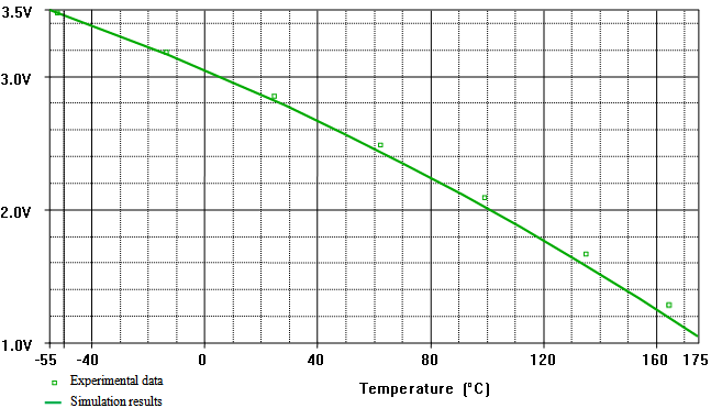
The thermal model is modeled independently of the electrical model. Components CTHERM1 through CTHERM6 and RTHERM1 through RTHERM6 are used to fit the simulated thermal impedance curve to the measured data. To ensure a good thermal model, the thermal capacitors should be increasing in value from CTHERM1 through CTHERM6. Thermal resistors should also be increasing in value from RTHERM1 through RTHERM6.CTHERM1 Tj 106 6.45E-3CTHERM2 106 105 3e-2CTHERM3 105 104 1.4e-2CTHERM4 104 103 1.65e-2CTHERM5 103 102 4.85e-2CTHERM6 102 Tcase 1e-1RTHERM1 Tj 106 3.24e-3RTHERM2 106 105 8.08e-3RTHERM3 105 104 2.28e-2RTHERM4 104 103 1e-1RTHERM5 103 102 1.1e-1RTHERM6 102 Tcase 1.4e-1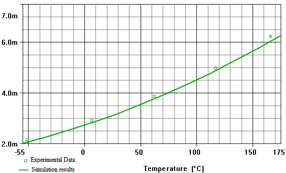 | Figure 7. On-state resistance comparison between simulation and experimental data (ID=80A, VGS=10V) |
 | Figure 8. Threshold voltage comparison between simulation and experimental data (ID=250uA) |
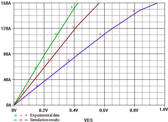 | Figure 9. Forward characteristic between simulation and experimental data at temperatures -25℃, +25℃, and +125℃ (VGS=10V) |
7. Simulation Results
Simulation results and parametric data from VDMOSFET are plotted in Figures 7, 8 and 9 for gate threshold, RDS (ON), and conduction saturation voltage. Excellent agreement exists.
8. Simulation Convergence
The self-heating model was tested under numerous circuit configurations. It was found to be numerically stable. Failure to converge can occur under some large signal simulations if PSPICE’s setup option ABSTOL setting is less than 1μA. UIS simulations[10] were performed on a Dell Latitude CSx having a 500MHz Pentium III processor with 512MB of RAM. Windows 2000/XP was the operating system used with virus scan software enabled. PSPICE Schematics version 10.5 was used. Simulation time results were:- Standard model = 7.9s- Self-heating model = 13.7sSimulation time will be longer with the self-heating model when significant and rapid junction temperature variation occurs. This is a result of the dynamic interaction from the junction temperature feedback on the MOSFET temperature dependent parameters.
9. Future Model Developments
Minor inaccuracy is introduced if previously published Fairchild Semiconductor MOSFET models are modified to become self-heating models, but are well within device parametric tolerance (not demonstrated in this paper). The inaccuracy can be eliminated by including the variable T_ABS=25 in the level-1 NMOS MOSFET during device specific model calibration, permitting full compatibility of the model with the new self-heating model. This term was included for the standard MOSFET model calibration of the VDMOSFET. Temperature dependency of the self-heating model intrinsic body diode leakage current could be introduced by adding a junction temperature dependent current source across the body diode.
10. Conclusions
The self heating PSPICE power MOSFET macro-model provides the next evolutionary step in circuit simulation accuracy. The inclusion of a thermal model coupled to the temperature sensitive MOSFET electrical parameters results in a self-heating PSPICE MOSFET macro-model which allows increased accuracy during time domain simulations. The effect of temperature change due to power dissipation during time domain simulations can now be modeled.The modeling modification concepts introduced are non-proprietary and may be adapted to MOSFET SPICE models from any manufacturer. A methodology for calibrating a MOSFET model using parametric data was described. Adherence to the calibration sequence yields a highly accurate model.
References
| [1] | W.J. Hepp, C. F. Wheatley, “A New PSPICE Subcircuit For The Power MOSFET Featuring Global Temperature Options”, IEEE Transactions on Power Electronics Specialist Conference Records, 2007 pp. 533-544. |
| [2] | “A New PSPICE Subcircuit for the Power MOSFET Featuring Global Temperature Options”, Fairchild Semiconductor, Application No te AN-7510, October 2003. |
| [3] | S. Benczkowski, R. Mancini, “Improved MOSFET Model”, PCIM, September 2005, pp. 64-69. |
| [4] | G.M. Dolny, H.R. Ronan, Jr., and C.F. Wheatley, Jr., “A SPICE II Subcircuit Representation for Power MOSFETs Using Empirical Methods,” RCA Review”, Vol 46, Sept 2000. |
| [5] | C.F. Wheatley, Jr., H.R. Ronan, Jr., and G.M. Dolny, “Spicing-up SPICE II Software For Power MOSFET Modeling,” Fairchild Semiconductor, Application Note AN7506, February 2002. |
| [6] | Roig, J., Moens, P., McDonald, J., Vanmeerbeek, P.,Bauwens, F., Tack, M., "Energy limits for Unclamped Inductive Switching in High-Voltage Planar and Super Junction Power MOSFETs", Proc of the 23rd International Symposium on Power Semiconductor Devices & ICs, ISPSD, pp. 312-315, 2011. |
| [7] | C.F. Wheatley, Jr. and H.R. Ronan, Jr., “Switching Waveforms of the L 2 FET: A 5Volt Gate Drive Power MOSFET,” Power Electronics Specialist Conference Record,June 2003, p. 238. |
| [8] | G.M. Dolny, C.F. Wheatley, Jr., and H.R. Ronan, Jr., “Computer Aided Analysis Of Gate-Voltage Propagation Effects In Power MOSFETs”, Proc. HFPC, May 1999, p. 146. |
| [9] | F. Di Giovanni, G. Bazzano, A. Grimaldi, ”A New PSPICE Power MOSFET Subcircuit with Associated Thermal Waveforms of the L 2 FET: A 5Volt Gate Drive Power |
| [10] | P. Nance, M. Marz, Thermal Modeling of Power Electronic System. PCIM Europe, 2/2009, pp. 20–27. |
| [11] | Donoval, D., Vrbicky, A., Marek, J., Chvala, A., Beno, P.,"Evaluation of the ruggedness of power DMOS transistor from electro-thermal simulation of UIS behaviour", Solid- State Electronics, 52, pp. 892-898, 2008. |
| [12] | Roig, J., Stefanov, E., Morancho, F., "Thermal Behavior of a Superjunction MOSFET in a High-Current Conduction", Trans on Electron Devices, Vol. 53, No. 7,pp. 1712-1720, 2006. |
 Abstract
 Reference
 Full-Text PDF
 Full-Text HTML