-
Paper Information
- Next Paper
- Paper Submission
-
Journal Information
- About This Journal
- Editorial Board
- Current Issue
- Archive
- Author Guidelines
- Contact Us
Microelectronics and Solid State Electronics
2012; 1(2): 21-25
doi: 10.5923/j.msse.20120102.01
FinFET with Constant Transconductance
 Abstract
 Reference
 Full-Text PDF
 Full-Text HTML
Samson Mil’shtein, John Palma
Advanced Electronics Technology Center, ECE Dept., UMass, Lowell, MA 01854
Correspondence to: Samson Mil’shtein, Advanced Electronics Technology Center, ECE Dept., UMass, Lowell, MA 01854.
| Email: |  |
Copyright © 2012 Scientific & Academic Publishing. All Rights Reserved.
Many analog FinFET applications, such as amplifiers, would benefit if the transistor provided a constant transconductance (gm=constant).The direct modification of transconductance can be done by tailoring the electric field inside the FinFET transistor. In the current study, we modeled and compared the electrical field profiles, IV characteristics, and transconductances of a conventional FinFET with a wrapped gate forming a single pair of gates, and our novel device with two wrapped gates forming two pairs of gates. We modeled and designed the devices taking into account transverse quantum confinement using the commercial modeling package Silvaco Atlas. We found that the novel FinFET operates with a nearly constant gmover a wide range of gate voltages. The novel device, made from silicon, has two pairs of gates with each gate being 10 nm wide and the two pairs of gates being 20 nm apart. The length of the transistor is 40 nm. The region underneath and between the gates is lightly n-type doped at 1×1015 cm-3 with doping of 7×1018 cm-3 at the source and drain contacts. The fin thickness is 120 Å and the gate oxide is 17 Å. The fin height is arbitrary as currents are normalized to the fin height.
Keywords: Mosfet, Finfet, Mugfet, Field Tailoring, Linearity
1. Introduction
- Rapid scaling down of silicon technology has resulted in the transformation of conventional planar Metal Oxide Semiconductor Field Effect Transistors (MOSFETs) into the vertical variant of Fin-shaped Field Effect Transistors (FinFETs).FinFETs are also known as Multi-Gate FETs (MuGFETs). However, this name creates confusion asmulti-gate planar FETs have been used in switches and field plate devices for quite some time. To avoid confusion with other multi-gate devices, we would like to suggest the name of “Wrapped Gate MOSFET (WG-MOSFET)”. This name better reflects the shape of the gateas it is physically wrapped around the fin. In the current study, we modeled and designed a FinFETwith two wrapped gates, hence referring to the device as a MuGFETwould create confusion.FinFETsoffer many well-known advantageswhich explain the recent focus on their R&D: the small dimensionsresult in devices that are free of short channel effects, electron quantizationresults in a one dimensional electron gas, and better control of carriers is achieved by using the wrapped gate[1-4]. The drawbacks of FinFETs,such as reduced electron velocity and unstable threshold voltage,are also well known[5-7]. Although the major fabrication steps originated with MOSFET technology, the typical selection of a (100) wafer orientation and a (110) channel direction causes a reduction of electron mobility. Widely used strained-layer technology is a very complicated[5,6] method and doesnot always bring the desired results. In this study, we recommend the field tailoring technique[8,9] to improve electron mobility and to linearize transconductance, gm. It is well established that electron mobility is decreased in FETs by up to a factor 14 as a result of the excessive internal electrical field along the channel of the transistor. Adjusting the electron mobility and gmby reshaping the electrical fieldhas proved to be a reliable method of improving these two parameters.The linearity of gm is a function of the uniformity of the electric field. Acceleration and deceleration of electrons in a non-uniform electric field is the major reason for the reduction of gm, and these changes of electron velocity cause non-linearity of the gain. Our recent modeling and experimental work[10,11] proved the concept not only in a laboratory environment, but also in commercial production. We demonstrated[11] that with a conventional fabrication process, a dual gate MOSFET design can be used to improve the gm and increase the mobility by applying a separate bias to each of the two gates, where the biases are chosen to result in optimal electric field conditions.FinFETs have emerged as a viable competitor for various analog applications[12-14]. The motivation of the current study is to use an additional wrapped gate to improve the linearity of the FinFET, via the field tailoring concept, which would be advantageous for many of these analog applications. Independently controlled gates have been previously employed by others to improve FinFET characteristics. The use of independently controlled gates was described for digital applications in[15,16], but these papers demonstrated independent control of each of the two transverse gates in conventional FinFETs. In addition, independent control of the two transverse gates was examined as a means to gain better control over the threshold voltage and sub-threshold swing[17]. This concept was extended by utilizing asymmetric gate-oxide thicknesses for further improvement of sub-threshold slopes[18]. It was shown in[19] that the asymmetric case offers better linearity as compared to the symmetric case. A structure similar to the one presented in this study, a quad gate (two sets of transverse gates) FinFET called the screen grid field effect transistor, was created to optimize transistor switching speeds for digital applications[20].
2. Challenges of FinFET Modeling
- With the trend in microminiaturization and the appearance of nano-scale devices, the task of modeling becomes very complicated due to the simultaneous presence of quasi-ballistic transport, quantization of carriers,and complicated boundary conditions along the device channel. Decades ago, the precision of Poisson simulators was a concern[21]. Nowadays, an answer is needed to thefundamental question on when and how the topology and equivalent circuitry of nano-devices change as the terminal voltages change. The detailed discussion of the modeling issues is beyond the scope of this paper, however, one should note the availability of numerous publications[7,22,23] which address quantum modeling in FinFETs of variable thicknesses through the use of the Green’s function and the use of matrix quantum mechanics in multi-gate HEMTs[24].Expecting that any specific modeling or commercially available design package won’t necessarily produce accurate results, we offer in this paper, a solution to the complicated issue of FinFET modeling. Using the commercial modeling package, Silvaco Atlas, we started with a device structure described recently by Yu et al.[2] and matched the output characteristics of the model to the experimentally published results. The major parameter which needed adjusting was the work function of the gate material. A strong dependence of the modeling outcome on the value of the work function is not surprising. Numerous experimental studies[4,25-27] demonstrated astrong dependence of FinFET performance on the selection of the work function of the gate material.
3. Design and Modeling
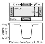
- To gain an improvement in FinFET linearity, the field tailoring concept is employed as was proven theoretically and experimentally by our group[8-11]. This concept states that since the strength and distribution of the electric field in a transistor is the most direct factor influencing device performance, modification of the electric field in the channel will lead to a modification of device performance. To obtain a flat transconductance, a more even electric field profile should be sought. The addition of a second wrapped gate provides the means for evening out this electric field across the device. By making the region in between the wrapped gates lightly doped, the electric field due to each of the wrapped gates is spread out somewhat over the higher resistance central region, further evening out and lessening the magnitude of the channel electric field. For this study, we modeled and compared the transconductances, I-V characteristics, and current gain of a conventional FinFET with one wrapped gate, and our novel device with two separately biased wrapped gates. The commercially available modeling package, Silvaco Atlas, was used. Modeling within this package involves selecting the physical description of the device in question, which includes the dimensions, material properties, and a selection of the physical models. Selecting the terminal conditions such as the biasing, results in the calculation of the resulting current or small signal response, and from these results, the desired information, such as transconductance or current gain can be plotted.For this study, transverse quantum confinement for both the single wrapped gate and the dual wrapped gate transistors was taken into account and the raw modeled results were passed through a Gaussian smoothing filter to eliminate any mathematical noise. The conventional single wrapped gate FinFET design was based on a previous publication by Yu et al.[2]. The modeling parameters were chosen so that the model’s results matched the experimental results given by Yu. Using these same parameters, the novel device was modeled so that it could be compared to the conventional FinFET. The novel device, shown in Figure 1, is made from siliconand has two wrapped gates, with each gate being 10 nm wide and the two wrapped gates being 20 nm apart. The length of the transistor is 40 nm. The region underneath and between the wrapped gates is lightly n-type doped at 1×1015 cm-3 with doping of 7×1018 cm-3 at the source and drain contacts. The doping profile was obtained from[22] where quantum modeling of the experimental device in[2] was performed.The fin thickness is 120 Å and the gate oxide thickness is 17 Å. The fin height is arbitrary as currents are normalized to the fin height.Figure 2 shows the standard FinFET device based on[2] and used as the point of reference. The gate width, fin thickness, and gate oxide thickness are the same as in the novel device. Also, the doping levels in the source, drain, and gate regions match those of the novel device.
 | Figure 1. Novel FinFET structure and doping profile |
 | Figure 2. Standard FinFET structure and doping profile |
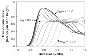 | Figure 3. Transcondutance of the novel FinFET for various differential biases, Vdiff = Vgate 2 – Vgate 1 |
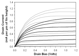 | Figure 4. Comparison between novel FinFET (black) and standard FinFET (grey) I-V curves with the gate bias ranging from Vg = +1.0 V (top curves) to Vg = -0.4 V (bottom curves) at 0.2V increments |
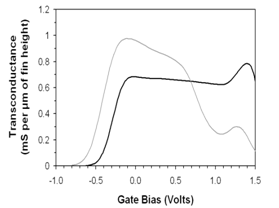 | Figure 5. Comparison between novel FinFET (black) and standard FinFET (grey) transconductances for Vd = 1.2 V |
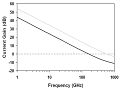 | Figure 6. Comparison of current gain for the novel (black) and standard (grey) devices |
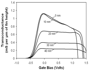 | Figure 7. Comparison of the transconductances of the novel configuration when changing the spacing between the two sets of gates from 0 nm (touching) to 40 nm. It is seen that at about 20 nm, flat transconductance is achieved. An increase in spacing does not affect flatness, but reduces the transconductance. If the spacing is too small, a flat transconductance is not achieved |
4. Conclusions
- In this study, a novel dual wrapped gate FinFET was modeled and designed. The model for the novel device used here was extended from a model of a standard FinFET that was based on previously published experimental results. Modeling results show that the novel device exhibits a nearly constant transconductance over its operating range. This is a consequence of the fact that the strength of electric field in the novel FinFET channel is much smaller than of that in the standard FinFET. The flat transconductance is largely invariant to most process variations, but the spacing between the wrapped gates must be chosen so that the transconductance remains flat and at a high magnitude. While the gain of the novel transistor is less than that of the standard example due to the increase in gate capacitance, the substantial improvement in linearity offers a favorable trade-off for many analog applications.