Microelectronics and Solid State Electronics

2012;  1(1): 15-20

doi: 10.5923/j.msse.20120101.03

Electronic Transport Properties of Junctionless Lateral Gate Silicon Nanowire Transistor Fabricated by Atomic Force Microscope Nanolithography

Farhad Larki 1, Sabar D. Hutagalung 2, Arash Dehzangi 1, E. B. Saion 1, Alam Abedini 1, A. Makarimi Abdullah 2, M. N. Hamidon 3, Jumiah Hassan 1

1Department of Physics, Faculty of Science, Universiti Putra Malaysia, Serdang, Selangor, 43400, Malaysia

2School of Materials and Mineral Resources Engineering, Universiti Sains Malaysia, Nibong Tebal, Penang, 14300, Malaysia,

3Department of Electrical and Electric Engineering, Faculty of Engineering, Universiti Putra Malaysia, Serdang, Selangor, 43400 , Malaysia

Correspondence to: Sabar D. Hutagalung , School of Materials and Mineral Resources Engineering, Universiti Sains Malaysia, Nibong Tebal, Penang, 14300, Malaysia,.

Email:

Copyright © 2012 Scientific & Academic Publishing. All Rights Reserved.

Abstract

We present the fabrication, electrical characteristics, and effect of lateral gates in a junctionless silicon nanowire transistor. The transistor uses silicon nanowire on silicon-on-insulator wafer fabricated with an atomic force microscope nanolithography technique. Using AFM nanolithography allows us to make a chemical contrast between locally oxidized part of the surface and unexposed surface. This chemical contrast affects as a mask and the active part of the device is finally obtained after two step etching. The structure is uniformly low-doped for source, drain, channel, and the lateral gates regions, and confirms the behavior of junctionless nanowire transistors. The output current is controlled by channel doping and mobility of carriers instead of gate capacitance and it basically uses bulk conduction instead of surface channel conduction. The fabricated device exhibits an on-off ratio of 2×10⁶ and a subthreshold swing of 160 mV/decade.

Keywords: Junctionless Silicon Nanowire Transistor, Lateral Gate, AFM Nanolithography, Silicon-On-Insulator (SOI)

1. Introduction

During the recent years, numerous efforts have been made to do real crossing from microelectronics to nanoelectronics and to persist with scaling imposed by Moore’s law. Several technological innovations and new materials such as high κ dielectrics[1], metal gate electrodes[2], and stressors[3] have been introduced in the fabrication process. Moreover, new transistor architectures based on silicon-on-insulator (SOI), such as FinFETs[4], multi-gate FETs[5], omega-gate FETs[6], and gate-all-around FETs[7] transistors have emerged. Photolithography approaches to the limitation of its potential[8], in terms of resolution and flexibility[9]. As an alternative among the low cost routes of lithography nano-contact printing technique and atomic force microscopy (AFM) nanolithography are the promising techniques. AFM lithography and scanning tunneling microscopy (STM) lithography are belong to a group of lithography called scanning probe lithography (SPL), which is considered as one of the best lithographic technique for forming nanostructures[10]. AFM lithography holds a distinct advantage over the STM because the exposure mechanism, typically an electric field or current, can be applied independently of the feedback control of the tip-sample spacing. Moreover, fabrication using AFM lithography can be done in liquid state as well as ambient environment, whereas STM lithography is mainly carried out in ultrahigh vacuum (UHV). In addition, AFM nanolithography provides more application such as, nano manipulation[11], force lithography[12], nano grafting[13], DPL[14], and nano oxidation[15]. The principle of AFM nanolithography on SOI has been described for the first time by Snow and Campbell et al.[16-17], and they astutely expanded AFM nanolithography for fabrication of nanostructures. Ionica et al[18] have remarkably reported the electrical characteristics of the devices made by AFM nanolithography. Recently, some new works are performed to improve the method of AFM nanolithography[19-20].
Fabrication of uniformly doped transistors which need no extra doping is another topic of interest and some groups already reported fabrication of structures such as accumulation metal oxide semiconductor FETs (AMOSFET)[21] and junctionless nanowire transistor (JLNWT)[22]. Fabrication of nanotransistors without junction and doping concentration was mainly considered by Shan et al[21]. Soon after that, a JLNWT was fabricated and characterized by the Tyndal group[22]. The idea behind this device is simplifying the source and drain engineering by removing the related junctions while, at the same time, sizing the silicon thickness and doping density in order to allow its switching under the gate voltage.
We already reported fabrication of the single lateral gate device with low doping concentration[23]. In this work we improved the method and used the advantages of AFM nanolithography in contact mode to fabricate a nanowire transistor device with a very simple structure calling it junctionless lateral gate silicon nanowire transistor (JLGSNWT). It requires only one doping type in all regions, which is taken here to be p-type. Electrical properties of the device are described based on the junctionless transistors model and conduction mechanism of the device is compared to the conventional MOSFETs.

2. Fabrication Process

The AFM nanolithography process was performed by using scanning probe microscope (SPM) machine (SPI3800N/4000). We have chosen to use the oxidation by AFM in contact mode. The main steps are schematically presented in Figure. 1 (a-d). This process was applied to a lightly doped ( 1015 cm-3) p-type (100) SOI prepared using Unibond™ process and a 145 nm buried oxide thickness [24]. The top Si layer has a thickness of 100 nm and a resistivity ρ of 13.5-22.5 Ω cm. In the fabrication process, the SOI wafer was cut into small sizes (1 cm 1 cm), cleaned by standard RCA cleaning process, and then dipped in hydrogen fluoride (HF) (1% water solution) for 30 seconds in order to replace the Si–O bonds by low energy Si–H bonds [25].
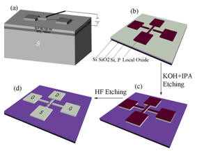
Figure 1. Schematic of fabrication steps: (a, b) AFM local oxidation in the contact mode. (c) Wet chemical etching of the unmasked silicon. (d) Removal of the local oxide mask by etching in HF.
A conductive AFM tip (Cr/Pt conductive coating) is used to draw pre-designed nanoscale oxide pattern of transistor structures. Hydrogen atoms can be locally removed with an AFM when a negative tip voltage is applied. It leads to a local oxidation of the substrate via a field-enhanced oxidation process by anodization. The oxidation reaction occurs only if tip voltage is chosen higher than a threshold of −2.7 V[26]. Applying an 8 V voltage to the tip, while it is scanning once over the silicon surface at speed of 1 µm/s, leads to a 2–3 nm-thick oxide pattern of width 90–95 nm. Figure 2(b) shows the structure with the best gate symmetry and the smallest reproducible dimensions we achieved. Since humidity is a very important parameter to form a water meniscus between the tip and surface, humidity was maintained in the range of 58-60%. We used a 30 wt% KOH solution, saturated with isopropyl alcohol (IPA) at 63 0C to remove all the non protected silicon areas.
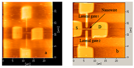
Figure 2. AFM images of the junctionless lateral gate silicon nanowire transistor before and after etching. After etching nanowire is 95 nm in width and 100 nm in height. The lateral gates are 100 nm away from the channel.
The IPA saturation decreases the etch rate, making the process more controllable, and gives very smooth surface[27]. The JLGSNWT was obtained by removing the oxide layer using HF (Figure. 2(b)). The most important advantage of AFM nanolithography is that it impedes damage of the crystalline structure of silicon due to highly energetic electrons which are normally introduced to the structure by techniques such as electron beam lithography[18].

3. Results and Discussion

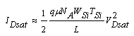
The electrical characteristics of the junctionless lateral gate silicon nanowire FET (JLGSNWT) measured by an HP4156c semiconductor parameter analyzer (SPA, Agilent) at room temperature are shown in Figure. 3(a). The family of the characteristic curves show that the drain current (ID) decreases with the positive increase of gate voltage (VG) from 0 to +2 V. This indicates that the transistor is p-channel field effect transistor. The device has a nanowire with constant width of 95 nm, while the nanowire thickness is fixed by the silicon top layer of the SOI sample (100 nm). Electrical connections are provided by two pads which can be considered as source and drain made of same doping as silicon nanowire. The lateral gates are two wires 200 nm wide connected at one end to a contact pad and at the other end separated by 100 nm from the nanowire. It is shown that, this gap can be reduced to 30 nm without noticeable current leakage[28-29]. The characteristic curves of the device show that the drain current magnitude first increases and then saturates, which is similar to those of a conventional MOSFETs characteristics however, the fundamental of operation is completely different.
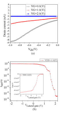
Figure 3. I-V characteristic of the device for different lateral gate voltages VG (a), Transfer characteristics with VDS= -1 V (b). The inset shows the linear IDS vs VG plot.
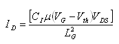
MOSFETs are normally off devices that drain current blocked by the reverse biased n/p or p/n junction at the drain. In the ON state, the inversion layer induced by gate voltage controls the drain current. The standard current expression for MOSFETs is given by[30]
(1)
where ID is the drain–current per device width, CI is the gate capacitance per area, μ is the channel mobility, VG is the gate–source voltage, Vth is the threshold voltage, VDS is the drain-source voltage, and LG is the channel length. The JLGSNWT, on the other hand, is basically a normally on device similar to the junctionless transistors. In recent reports on experimental JLNWTs[31-32] we did not encounter any case of ON state condition under the zero gate voltage, unless for the simulation cases and for very small gate lengths[33]. The reason can arise from the fact that the field effect from the work function of the gate, in the case of JLGSNWT, cannot cause the device to turn off at VG = 0 V due to low concentration profile of the channel, the position of lateral gates with no conventional oxide semiconductor connection, and the channel dimension.
When the device is biased in the ON state, the hole concentration in the channel increases and the neutral (undeleted) channel forms between source and drain, in the center of channel, until the peak of the hole concentration in the channel reaches the doping concentration NA. when the device is turned on it approaches the flat band condition, thus, it basically behaves as a resistor and the electric field perpendicular to the current flow is basically equal to zero in the ‘‘bulk’’ channel[22]. In fact, as the advantage of the AFM nanolithography the body of the upper Si layer of the SOI, intact and untouched. So we expect to find more bulk property, higher mobility, and less surface scattering effect for the channel under the gate. Moreover, since the system is in ON at VG=0 V, one can say that the threshold voltage is shifted into the positive voltage. That is the reason one can claim the device is like the pinch off transistors and is already in flatband condition[34].
With increasing the positive gate voltage, area under the gates starts to deplete and a sufficient positive bias applied to the gate completely depletes the region. Due to the same doping of structure the channel under the gates cannot invert easily. Even if it were to invert, the reverse bias p-region contacting this inversion layer (-VDS), would limit the transport in this layer. Figure 3(b) shows the drain current (ID) versus gate voltage (VG), for a drain voltage of -1 V. The on/off current ratio for gate voltage between 0 and 2 V is around 2×10⁶ for a device with 95 nm width and 100 nm gate gaps.
Below threshold voltage of the device, it is possible to apply a sufficient negative gate bias (–VG) to create an accumulation channel and increase the output current (not shown). In this case the gate acts as a backgate and accumulates the region under the gates. These results are in agreement with the basic theory of junctionless transistors and results obtained and reported by simulation[33] and experimental results[32] in the literature.
Figure 4.1 shows the simple comparison between the AMOSFET and JLGSNWT holes transmission location path through the channel. It is worth to mention that, due to the device design the accumulation channel will be formed at the bottom of the channel which is the Si/SiO2 interface.
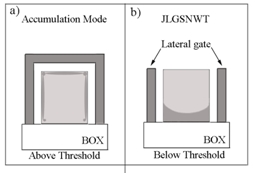
Figure 4. Hole location transmission path in (a) AMOSFET and (b) JLGSNWT.
Normally in high doping JLNWTs by increasing the gate voltage above flatband the device is able to be converted into the accumulation mode and have remarkable increasing of the current, but mostly is not desired to reach[22, 32]. We didn’t observed significant increase in the output current above flatband. The reason can be explained by the fact that the doping concentration is low in the channel and contacts. Accordingly, they cannot prepare enough charges to increase the current.
We used the model developed for calculating the body current of accumulation-mode transistor with the glance in JLNWT theory. This model already used for AMOSFETs[21] and JLNWTs[22]. Since the device behaves as a resistor when it is turned on and in flatband conditions the drain current is given by
(2)
where Wsi is the width of the silicon, TSi is the thickness of the silicon, L is of the order of LG, and NA is the doping concentration. It is clearly observed that in addition to the nanowire dimension, the carrier’s mobility and doping density are two determinant factors.
The subthreshold swing (SS) is defined as the inverse of the slope of the log of the drain current versus gate voltage below threshold. Typical bulk MOS transistors have a subthreshold slope on the order of 80 mV/decade, and the best tri-gate SOI transistors has SS of about 63 mV/decade, which is close to the theoretical value of 60 mV/decade[35]. We used model for thin SOI films which considers the potential contribution of the native oxide interface[18, 36]:
(3)
where 
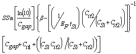
, Cgap is the capacitance of the air in the gap between channel and the gate, EF is the electric field at the Si-air interface, tSi is the thickness of top silicon layer, Cit1 is the capacitance due to the interface state density between the top silicon and the air, and Cit2 is the capacitance due to the interface state density between the top silicon and the native oxide. Since for the case of fresh sample there is no native oxide that we can consider, Cit2=0. For a top silicon thickness of 100 nm, width of 95 nm, and gate gap of 100 nm Equation (3) gives SS ≈200 mV/decade. The variance between the subthreshold swing measured from the transfer characteristic and calculated by Equation (3) can be explained by considering the effect of Si/air capacitance in the calculation. In JLNWT now it is well known that even the SiO2 capacitance has a negligible effect on the behavior of the device. The gaps between the lateral gates and the channel and the channel width reduce the effect of gates and it is the reason of high subthreshold swing of the device. Closer gates to channel distances, gates with larger cross sections, and channel with smaller cross section are critical parameters in order to achieve near ideal subthreshold swing in this structures.

4. Conclusions

We presented here the electrical characteristics of lightly doped junctionless lateral gate silicon nanowire transistors. The fabrication method used is based on AFM nanolithography on SOI substrate. The performance of device is compared to junctionless nanowire transistors. This device is a normally on device which has an off state base on depletion of the channel by electric field originated from the lateral gates. Output current of the device increases strongly with active region doping density and carriers’ mobility and it is not depends on the gate capacitance. The device uses bulk conduction instead of surface conduction. Controlling the cross section and gate gaps are key parameters for better performance of the device and particularly for subthreshold swing tuning.

ACKNOWLEDGEMENTS

The authors gratefully acknowledge that this work was financially supported by the Science Fund from the Ministry of Science, Technology and Innovation (MOSTI), Malaysia, under project no. 03-01-05-SF0384, the USM Short Term Grant under project no. 304/PBAHAN/6039035, and UPM FRGS no. 5524051

References

[1]  C. Lee, S.Y. No, D.I. Eom, C.S. Hwang, H.J. Kim, "The electrical and physical analysis of Pt gate/Al2O3/p-Si (100) with dual high-k gate oxide thickness for deep submicron complementary metal-oxide-semiconductor device with low power and high reliability", Springer, Journal of Electronic Materials, Vol. 34, pp. 1104-1109, 2005.
[2]  R. Chau, S. Datta, M. Doczy, B. Doyle, J. Kavalieros, M. Metz,"High-k/metal-gate stack and its MOSFETcharacteristics", IEEE-INST ELECTRICALELECTRONICS ENGINEERS INC, IEEE, Electron Device Letters, Vol. 25, pp. 408-410, 2004.
[3]  Y. Song, H. Zhou, Q. Xu, J. Luo, H. Yin, J. Yan, H. Zhong, "Mobility Enhancement Technology for Scaling of CMOS Devices: Overview and Status", Springer, Journal of Electronic Materials, pp. 1-29, 2011.
[4]  G. Lansbergen, R. Rahman, C. Wellard, I. Woo, J. Caro, N. Collaert, S. Biesemans, G. Klimeck, L. Hollenberg, S. Rogge, "Gate-induced quantum-confinement transition of a single dopant atom in a silicon FinFET", NATURE PUBLISHING GROUP, Nature Physics, Vol. 4, pp. 656-661, 2008.
[5]  J. Colinge, "Multi-gate SOI MOSFETs", ELSEVIER SCIENCE BV, Microelectronic engineering, Vol. 84, pp. 2071-2076, 2007.
[6]  Y. Li, H.M. Chou, J.W. Lee, "Investigation of electrical characteristics on surrounding-gate and omega-shaped-gate nanowire FinFETs", IEEE-INST ELECTRICALELECTRONICS ENGINEERS INC, IEEE Transactions on Nanotechnology, Vol. 4, pp. 510-516, 2005.
[7]  B. Yang, K. Buddharaju, S. Teo, N. Singh, G. Lo, D. Kwong, "Vertical silicon-nanowire formation and gate-all-around MOSFET", IEEE-INST ELECTRICAL ELECTRONICS ENGINEERS INC, IEEE, Electron Device Letters, Vol. 29, pp. 791-794, 2008.
[8]  C. Srinivasan, M. Anderson, E. Carter, J. Hohman, S. Bharadwaja, S. Trolier-McKinstry, P. Weiss, M. Horn, "Extensions of molecular ruler technology for nanoscale patterning", A V S AMER INST PHYSICS, Journal of Vacuum Science & Technology B: Microelectronics and Nanometer Structures, Vol. 24, pp 3200, 2006.
[9]  Y.H. Wang, C.A. Mirkin, S.J. Park, "Nanofabrication beyond electronics", AMER CHEMICAL SOC, ACS nano, Vol. 3, pp. 1049-1056, 2009.
[10]  S. Lee, J. Kim, W.S. Shin, H.J. Lee, S. Koo, H. Lee, "Fabrication of nanostructures using scanning probe microscope lithography", ELSEVIER SCIENCE BV, Materials Science and Engineering: C, Vol. 24, pp. 3-9, 2004.
[11]  D. Sheglov, A. Latyshev, A. Aseev,"The deepness enhancing of an AFM-tip induced surface nanomodification", ELSEVIER SCIENCE BV, Applied surface science, Vol. 243, pp. 138-142, 2005.
[12]  C.H. Choi, D.J. Lee, J.H. Sung, M.W. Lee, S.G. Lee, S.G. Park, E.H. Lee, "A study of AFM-based scratch process on polycarbonate surface and grating application", ELSEVIER SCIENCE BV, Applied surface science, Vol. 256, pp. 7668-7671, 2010.
[13]  S. Xu, S. Miller, P.E. Laibinis, G. Liu, "Fabrication of nanometer scale patterns within self-assembled monolayers by nanografting", AMER CHEMICAL SOC, Langmuir, Vol. 15, pp. 7244-7251, 1999.
[14]  D. Roy, M. Munz, P. Colombi, S. Bhattacharyya, J.P. Salvetat, P. Cumpson, M.L. Saboungi, "Directly writing with nanoparticles at the nanoscale using dip-pen nanolithography", ELSEVIER SCIENCE BV, Applied surface science, Vol. 254, pp. 1394-1398, 2007.
[15]  J. Cervenka, R. Kalousek, M. Bartosik, D. Skoda, O. Tomanec, T. Sikola, "Fabrication of nanostructures on Si (1 0 0) and GaAs (1 0 0) by local anodic oxidation", ELSEVIER SCIENCE BV, Applied surface science, Vol. 253, pp. 2373-2378, 2006.
[16]  P. Campbell, E. Snow, P. McMarr, "Fabrication of nanometer scale side gated silicon field effect transistors with an atomic force microscope", AMER INST PHYSICS, Applied Physics Letters, Vol. 66, pp. 1388, 1995.
[17]  E. Snow, P. Campbell, P. McMarr, "Fabrication of silicon nanostructures with a scanning tunneling microscope", AMER INST PHYSICS, Applied Physics Letters, Vol. 63, pp. 749-751, 1993.
[18]  I. Ionica, L. Montes, S. Ferraton, J. Zimmermann, L. Saminadayar, V. Bouchiat, "Field effect and Coulomb blockade in silicon on insulator nanostructures fabricated by atomic force microscope", PERGAMON-ELSEVIER SCIENCE LTD, Solid-State Electronics, Vol. 49, pp. 1497-1503, 2005.
[19]  G. Pennelli, "Top down fabrication of long silicon nanowire devices by means of lateral oxidation", ELSEVIER SCIENCE BV, Microelectronic engineering, Vol. 86, pp. 2139-2143, 2009.
[20]  J. Martinez, R.V. Martínez, R. Garcia, "Silicon nanowire transistors with a channel width of 4 nm fabricated by atomic force microscope nanolithography", AMER CHEMICAL SOC, Nano Letters, Vol. 8, pp. 3636-3639, 2008.
[21]  Y. Shan, S. Ashok, S.J. Fonash, "Unipolar accumulation-type transistor configuration implemented using Si nanowires", AMER INST PHYSICS, Applied Physics Letters, Vol. 91, pp. 093513-093518, 2007
[22]  J.P. Colinge, C.W. Lee, A. Afzalian, N.D. Akhavan, R. Yan, I. Ferain, P. Razavi, B. O'Neill, A. Blake, M. White, "Nanowire transistors without junctions", NATURE PUBLISHING GROUP, Nature Nanotechnology, Vol. 5, pp. 225-229, 2010.
[23]  A. Dehzangi, F. Larki, E. Saion, S.D. Hutagalung, M. Hamidon, J. Hassan," Field effect in silicon nanostructure fabricated by Atomic Force Microscopy nano lithography", in Proceedings of 2011 IEEE Regional Symposium on Micro and Nano Electronics, pp. 104-107, 2011.
[24]  P.T.F. SOITEC, 38190 Bernin, France, in.
[25]  W. Kern, Handbook of semiconductor wafer cleaning technology: science, technology, and applications, Noyes Pubns, 1993.
[26]  D. Stievenard, P. Fontaine, E. Dubois,"Nanooxidation using a scanning probe microscope: An analytical model based on field induced oxidation", AMER INST PHYSICS, Applied Physics Letters, Vol. 70, pp. 3272, 1997.
[27]  I. Zubel, M. Kramkowska, "Etch rates and morphology of silicon (hkl) surfaces etched in KOH and KOH saturated with isopropanol solutions", ELSEVIER SCIENCE BV, Sensors and Actuators A: Physical, Vol. 115, pp. 549-556, 2004.
[28]  N. Clement, D. Tonneau, H. Dallaporta, V. Bouchiat, D. Fraboulet, D. Mariole, J. Gautier, V. Safarov,"Electronic transport properties of single-crystal silicon nanowires fabricated using an atomic force microscope", ELSEVIER SCIENCE BV, Physica E: Low-dimensional Systems and Nanostructures, Vol. 13, pp. 999-1002, 2002.
[29]  V. Bouchiat, M. Faucher, T. Fournier, B. Pannetier, C. Thirion, W. Wernsdorfer, N. Clement, D. Tonneau, H. Dallaporta, S. Safarov, "Resistless patterning of quantum nanostructures by local anodization with an atomic force microscope", ELSEVIER SCIENCE BV, Microelectronic engineering, Vol. 61, pp. 517-522, 2002.
[30]  S.M. Sze, Semiconductor devices: physics and technology, Wiley-India, 2009.
[31]  J.P. Raskin, J.P. Colinge, I. Ferain, A. Kranti, C.W. Lee, N.D. Akhavan, R. Yan, P. Razavi, R. Yu, Mobility improvement in nanowire junctionless transistors by uniaxial strain, AMER INST PHYSICS, Applied Physics Letters, Vol. 97, pp. 042114, 2010.
[32]  J. Colinge, C. Lee, N. Dehdashti Akhavan, R. Yan, I. Ferain, P. Razavi, A. Kranti, R. Yu, Junctionless Transistors: Physics and Properties, Semiconductor-On-Insulator Materials for Nanoelectronics Applications, Springer, Verlag Berlin Heidelberg, 2011.
[33]  L. Ansari, B. Feldman, G. Fagas, J.P. Colinge, J.C. Greer, Simulation of junctionless Si nanowire transistors with 3 nm gate length, AMER INST PHYSICS, Applied Physics Letters, Vol. 97, pp. 062105, 2010.
[34]  D. Sels, B. Sorée, G. Groeseneken, Quantum ballistic transport in the junctionless nanowire pinch-off field effect transistor, Springer, Journal of computational electronics, pp. 1-6, 2011.
[35]  C.W. Lee, D. Lederer, A. Afzalian, R. Yan, N.D. Akhavan, J.P. Colinge, Analytical model for the high-temperature behaviour of the subthreshold slope in MuGFETs, ELSEVIER SCIENCE BV, Microelectronic engineering, vol. 86, pp. 2067-2071, 2009.
[36]  H. Hovel, Si film electrical characterization in SOI substrates by the HgFET technique, PERGAMON-ELSEVIER SCIENCE LTD, Solid-State Electronics, vol. 47, pp. 1311-1333 2003.