Rohan Kumbhare , Jitendra Kanungo , A. K. Saxena , S. Dasgupta
Microelectronics and VLSI Technology Group, Indian Institute of Technology Roorkee, Roorkee (Uttrakhand), 247667, India
Correspondence to: A. K. Saxena , Microelectronics and VLSI Technology Group, Indian Institute of Technology Roorkee, Roorkee (Uttrakhand), 247667, India.
| Email: |  |
Copyright © 2012 Scientific & Academic Publishing. All Rights Reserved.
Abstract
This paper presents low power clock gating adiabatic D flip-flop using single phase sinusoidal power clock scheme. We propose the clock gated single phase Quasi-Static Energy Recovery Logic (QSERL) D flip-flop at 90nm CMOS technology. In the previously proposed QSERL logic, two phase sinusoidal power clocks were used that increased the hardware complexity and clocking issues. In this paper, single phase QSERL is proposed to reduce the hardware complexity and clocking issues. The clock gating technique is applied to a QSERL D flip-flop during idle periods of clock. The proposed scheme works efficiently with reduced power loss. All the simulations have been performed using Cadence spectre simulator.
Keywords:
Low Power, Clock Gating, Adiabatic Switching, Energy Recovery and QSERL
1. Introduction
As the density and operating speed of CMOS chips increases, the power dissipation becomes a critical concern[1]. In order to minimize the power dissipation, research at various levels of design is going on which reports ultra low power dissipation with optimum performance. The dynamic power dissipation in a circuit is due to charging and discharging of output node capacitance(s). Different charging and discharging paths cause the energy to be dissipation in the form of heat. An adiabatic switching technique reduces the dynamic power dissipation by recycling the charge stored in the node capacitance. This recycling is achieved by using an AC power source instead of the constant DC power source[2]. The power dissipation is reduced by maintaining a very low potential difference across the two terminals of a turn-on MOS device. The previously reported adiabatic circuits demand mostly multi-phase power clocks. The problems of multi-phase clocking adiabatic circuits include the issues such as: clock skew, complicated power clock tree and multiple power clock generators, which results in extra area overhead and increases the hardware complexity[3].The static CMOS circuit shows negligible dynamic power loss as long as input signal does not switch. In adiabatic or energy recovery logic, the clock generator circuit continuously provides clock signal resulting in dynamic power dissipation. The clock gating is most efficient way to reduce power dissipation in clocked logic circuits. This technique detaches the clock generator circuit from the logical circuit when circuit is in idle mode. However, in adiabatic circuits, energy dissipation occurs even if the input signals are not being switched since their output nodes are always charged and discharged by power clock[4]. Similar to power gating and clock gating techniques of conventional CMOS circuits, the energy loss can be reduced during idle periods of adiabatic units by switching off their power clocks. Several clock gating schemes for adiabatic circuits have been proposed and achieved considerable energy savings[5-10]. It is reported that, previously described clock gating adiabatic flip-flop was designed using the multi-phase clock schemes. This paper presents clock gating flip-flops using single-phase quasi-static energy recovery scheme.
2. An Overview of Quasi-Static Energy Recovery Logic (QSERL)
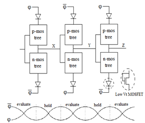 | Figure 1. Two-Phase QSERL[6] |
QSERL scheme is shown in Fig. 1 that resembles the static CMOS logic. QSERL uses two additional diodes and two sinusoidal clocks in complementary phases. The diode on the top of PMOS tree controls the charging path, while other diode at the bottom of NMOS tree controls the discharging path. Quasi-static energy recovery logic (QSERL) which uses two complementary sinusoidal supply clocks possesses several positive characteristics of static CMOS logic. The lower switching activity reduces energy dissipation. QSERL circuits can be directly converted from static CMOS circuits without drastically increasing the circuit complexity and transistor overheads.The circuit operates in a nearly adiabatic fashion. A QSERL gate is based on a static CMOS gate with two additional diodes. Two sinusoidal clocks in complementary phases, Φ and  , are sufficient. Hence, the complexity in circuit wiring and design are greatly reduced compared to other energy recovery logic families. The supply clock signal consists of two phases, evaluation and hold, as shown in Fig. 1. Let us consider the first gate in Fig. 1. In evaluation phase, Φ swings up while
  swings down. In one of the two paths, the pMOS pull-up tree or nMOS pull-down tree is turned ON. There are four cases as follows:1) The circuit input node is LOW and the pMOS tree is turned ON. Then output follows Φ as it swings HIGH.2) The circuit input node is LOW and the nMOS tree is ON. Output remains LOW and no transition occurs.3) The circuit input node is HIGH and the pMOS tree is ON. Output remains HIGH and no transition occurs.4) The circuit input node is HIGH and the nMOS tree is ON. Output follows Φ down to LOW.In the hold phase, Φ swings down while
  swings up. The circuit output node remains unchanged due to the diodes. Note that cascaded gates are in alternate phases. The second gate in Fig. 1 evaluates its logic value while the first gate is in hold phase. Advantages of this QSERL include the simplicity and its similarity to static CMOS. In contrast to dynamic energy recovery logic in which each gate charges and discharges in every cycle, QSERL is “static.” Circuit nodes are not necessarily charging and discharging every clock cycle, thus reducing the node switching activity substantially.
 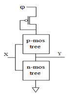 | Figure 2. Proposed Single-Phase QSERL |
Thus, lower switching activity in QSERL logic reduces energy dissipation. The diodes used in QSERL for controlling the charging and discharging paths can be implemented by low-threshold voltage MOSFETs when low-threshold diodes are not available. Note that cascaded gates are in alternate phases. The second gate in Fig. 1 evaluates its logic while first one is in hold phase[6].MOSFETs with gate and drain shorted having low- threshold voltage can be used instead of diodes used for controlling the charging and discharging paths.
3. Proposed QSERL
The QSERL as shown in Fig. 1 uses two phase power clocks. The charging and discharging device puts one threshold voltage drop at the output ,thus, output voltage does not gain full voltage swing i.e. 0 to VDD. There is VT threshold drop from upper as well as lower side in output voltage in QSERL which results in output swing from VDD-VT to VT. In this paper, single-phase QSERL circuit (Fig.2) is proposed that avoids overhead of multi-phase power clock generator circuit and is also able to reduce the power dissipation. In single phase QSERL, one power clock with NMOS transistor placed at the bottom has been removed. It results i anincrease in output voltage swing i.e. from 0 to VDD-VT. An advantage of this circuit is that it increases output voltage swing and keeps the power advantage of reported QSERL. When output of logical block is switching from logic 0 to logic 1, voltage across turned-on PUN is zero or minimum. So minimum power is dissipated in switching from logic ‘0’ to logic ‘1’. But for logical switching from logic ‘1’ to logic ‘0’, circuit will not work adiabatically. Therefore, this single phase QSERL easily resembles to static CMOS logic.In static CMOS circuit, dynamic loss does not occur as long as input signal is constant. But in adiabatic circuits, there is dynamic power dissipation with clock generation because energy stored at output node is continuously charged and discharged with clock signal. So in order to avoid the power loss of an adiabatic logic for idle mode of input signals ,the logical block should be detached from energy recovery clock generator. One PMOS transistor is introduced to detach logic block from energy recovery supply when input signal is not changing. The circuit behaviour is same as for reported QSERL and is able to store the input information. The proposed circuit reduces the power dissipation at the cost of speed and enables ultra low power digital circuit design.
4. Clock Gating
In adiabatic logic, the clock generator circuit continuously provides the clock even when the input signal is not changing i.e. logical circuit is in idle mode that results in loss of power. Clock gating is an efficient way to reduce power dissipation in the adiabatic logic circuit. It detaches clock generator circuit from logical block during idle periods. The clock signal and distribution in a sequential system is a major contributor to the power dissipation which is the only signal that switches all the time. In addition, the clock signal tends to be highly loaded. To distribute the clock and control the clock skew, one needs to construct a clock network (often a clock tree) with clock buffers. All of this adds to the capacitance of the clock net. Recent studies indicate that the clock signals in digital computers consume a large (15–45%) percentage of the system power. Thus, the circuit power can be greatly reduced by reducing the clock power dissipation. In many cases, switching of the clock causes a great deal of unnecessary gate activity. For that reason, circuits are being developed with controllable clocks. This means that from the master clock, other clocks are derived which, based on certain conditions, can be slowed down or stopped completely with respect to the master clock. Obviously, this scheme results in power savings due to the following factors[11].1) The load on the master clock is reduced and the number of required buffers in the clock tree is decreased. Therefore, the power dissipation of clock tree can be reduced.2) The flip flop receiving the derived clock is not triggered in idle cycles and the corresponding dynamic power dissipation is thus saved.3) The excitation function of the flip flop triggered by the derived clock may be simplified since it has a ‘don’t care’ condition in the cycle when the flip flop is not triggered by the derived clock.The reliable flip-flop is realized using clock gating and single phase QSERL method which is shown in Fig. 3. Clock gating method is implemented using comparator and gating circuits. In D flip-flop, comparator includes XOR gate which compares D and Q, while the gating logic includes simple AND gate at the input of which ck signal and comparator output is applied.· When ck=0, node ‘ckg’ is pulled high. During the subsequent high level of the ck signal, two different situations are possible[7]. · As D is different from Q, comp becomes equal to 1 and node ‘ckg’ is pulled down. Afterward when ck goes to 0, a positive edge of ‘ckg’ is produced.· Suppose comp is always equal to 0 and ck=1, ‘ckg’ node is not pulled down and hence no active edge of ck is produced even when ck goes to 0. For ck=1 and comp=0 the gating logic is in a memory state.In this paper, NC2MOS Gating has been applied that uses only one gating logic for the whole flip-flop and hence reduces the gating logic overhead. The schematic of NC2MOS gating logic for negative edge triggered flip-flop is shown in Fig. 4. Structure uses a pull-up net, for  node, realized by only one PMOS driven by ck signal. In this way, only the clock ck and not comp can drive negative edge on ‘ckg’, so that the flip-flop can be activated only by ck.The schematic for positive edge triggered flip-flop is quite similar. The difference is in pull-down net, which is composed of a single NMOS driven by ck and in the pull-up net which presents two series PMOS, one driven by ck and other by signal ‘comp’.Above explained gating method was for clock generator circuit. Same gating method can also be used for D-ff. PMOS transistor is connected between power supply and inverters of D-ff which acts as gating for power supply. Output of clock gating i.e.
  is connected to the gate of this PMOS transistor. So this PMOS switch is turned-on only when D-ff is triggered by clock gating circuit.
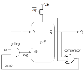 | Figure 3. D flip-flop with clock gating. |
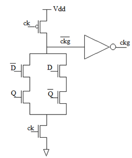 | Figure 4. NC2MOS Gating for Negative Edge Triggered D-ff[7]. |
5. Simulations Results and Discussions
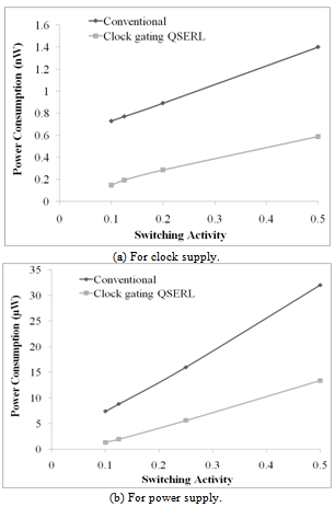
Proposed D flip-flop circuit is designed and implemented at 90nm CMOS technology with 1.2V supply voltage and compared with a conventional static CMOS D flip-flop at clock frequency of 100MHz. The comparison circuit is a master- slave flip-flop with simple static transmission gate latches. An inverter has been included in the flip-flop to produce the inverted clock signal.Simulation result of D-ff has been obtained through CADENCE spectre simulator as shown in Fig. 5. Power dissipation as a function of input switching activity at frequency of 100MHz has been calculated and plotted for both circuits as shown in Fig. 6. It is observed that power dissipation in conventional D-ff rapidly increases with switching activity but this is not the case in clock gating QSERL D-ff. Fig. 7 shows power loss of D-ff for different frequencies at switching activity of 0.1.We have designed SIPO 4-bit shift register as shown in Fig. 8 based on the clock gating and single phase QSERL technique to show an efficiency of the proposed technique. Its simulated waveform is shown in Fig. 9. Comparison of power consumption of 4-bit shift register using clock gating and single phase QSERL with conventional static CMOS method at different frequency is shown in Fig. 10. | Figure 5. Simulated waveform of clock gating adiabatic D-ff |
 | Figure 6. Power consumption as a function of input signal switching activity for D-ff. Clock frequency is 100MHz. |
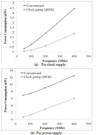 | Figure 7. Power Consumption of D-ff for different frequencies at switching activity of 0.1. |
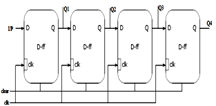 | Figure 8. 4-bit Shift Register. |
It is observed that power saving of the proposed shift register is about 70% for clock supply and it is about 82% for power supply at frequency of 100MHz.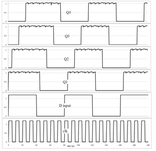 | Figure 9. Waveforms of 4-bit shift register. |
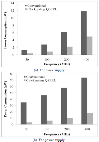 | Figure 10. Comparison of power consumption of clock gating QSERL with conventional 4-bit shift register |
6. Conclusions
This work makes it easier to choose adiabatic logic with clock gating in achieving ultra low power digital logic circuit. The clock gating techniques succeeds in disabling proposed QSERL D flip-flop during idle periods and does not exhibit timing issues. Dynamic power dissipation during idle periods has been reduced in significant amount. Shift register has also been designed and obtained results show workability of clock gated adiabatic D flip-flop. Reliable flip-flops and sequential circuits can be realized with clock gating and single phase QSERL method.
ACKNOWLEDGEMENTS
One of us (RK) is thankful to MHRD for a fellowship. The work was carried out in VLSI Design Laboratory of the department. We are also thankful to MIT, Government of India for supporting the phase-II of Special Manpower Development Programme in the department.
References
| [1] | Chandrakasan, A. P. S. Sheng and R.W. Brodersen, “Low-power CMOS digital design,” IEEE Journal of Solid-State Circuits, Vol. 27(4), pp. 473-483, 1992. |
| [2] | A.G. Dickinson and J.S. Denker, “Adiabatic dynamic logic,” IEEE Journal of Solid- State Circuits, Vol. 30, pp. 311-315, 1995. |
| [3] | S. Kim and M. C. Papaefthymiou, “True single phase adiabatic circuitry,” IEEE Trans. on VLSI Syst., Vol. 9, pp. 52-63, 2001. |
| [4] | Changing luo and Jianping Hu, “Single-phase adiabatic flip-flops and sequential circuits using improved CAL circuits,” IEEE ASICON’07, Guilin, China, pp. 126-129, 2007. |
| [5] | Jianping Hu, Dong Zhou and Ling Wang, “Power gating adiabatic flip-flops and sequential logic circuits,” IEEE ICCCAS’07, Fukuoka, Japan, pp. 1016-1020, 2007. |
| [6] | Y. Ye and K. Roy and G. Stamoulis, “Quasi-static energy recovery logic and supply clock generation circuits,” in IEEE/ACM Int. Symp. Low Power Electronics and Design, Monterey, CA, pp. 96-99, 1997. |
| [7] | A.G.M. Strollo, E. Napoli and D. De Caro, “New clock-gating techniques for low power flip-flops,” IEEE ISLPED’00, Rapallo, Italy, pp. 114-119, 2000. |
| [8] | W. Zhang, D. Zhou, X. Hu and J.Hu, “The implementations of adiabatic flip-flops and sequential circuits with power-gating schemes,” IEEE 51st Midwest Symp.C ircuits and Systems, MWSCAS 2008, Knoxville, Tennessee, pp. 767 – 770, 2008. |
| [9] | Haiyan Ni and Jianping Hu, “Single-phase adiabatic flip-flops and sequential circuits with power-gating scheme,” IEEE 8th Int. Conf. ASIC ASICON '09, Changsha, Hunan Sheng, China, pp. 879-882, 2009. |
| [10] | Weiqiang Zhang, Yu Zhang, Shi Xuhua and Jianping Hu, “Leakage Reduction of Power-Gating Sequential Circuits Based on Complementary Pass-Transistor Adiabatic Logic Circuits” IEEE Int. conf. Innovative Computing & Communication, Macao, pp. 282 – 285, 2010. |
| [11] | Qing Wu, Massoud Pedram, and Xunwei Wu, “Clock-Gating and Its Application to Low Power Design of Sequential Circuits” IEEE Trans. on Circuits And Systems—I: Fundamental Theory And Applications, vol. 47, no. 103, pp. 415-420, March 2000 |
 Abstract
 Reference
 Full-Text PDF
 Full-Text HTML