-
Paper Information
- Next Paper
- Paper Submission
-
Journal Information
- About This Journal
- Editorial Board
- Current Issue
- Archive
- Author Guidelines
- Contact Us
Microelectronics and Solid State Electronics
2012; 1(1): 1-8
doi: 10.5923/j.msse.20120101.01
Early Voltage and Current Gain of Si1-yGey Heterojunction Bipolar Transistor
 Abstract
 Reference
 Full-Text PDF
 Full-Text HTML
Fazle Rabbi , Yeasir Arafat , M. Ziaur Rahman Khan
Department of EEE, BUET, Dhaka, 1000, Bangladesh
Correspondence to: Yeasir Arafat , Department of EEE, BUET, Dhaka, 1000, Bangladesh.
| Email: |  |
Copyright © 2012 Scientific & Academic Publishing. All Rights Reserved.
Closed form analytical models were derived for Early voltage (VA) and common emitter current gain (β) for Si1-yGeyHeterojunction Bipolar Transistor (HBT). Field dependent mobility, doping dependent mobility, band gap narrowing (BGN) effect (due to both heavy doping and presence of Germanium content in the base) and velocity saturation effects were considered in these models. The derived models are applicable for uniform, exponential and Gaussian types of base doping profiles and trapezoidal, triangular or box germanium profiles.The variations of VA, β, intrinsic carrier concentration, diffusivity and electric field in the base region with the variation of germanium mole fraction were studied. The results obtained by these analytical models were compared with the results available in the literature and found in good agreement.
Keywords: Early Voltage and Current Gain, Field Dependent Mobility, Gaussian Profile, SiGe base HBT
Article Outline
1. Introduction
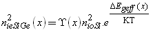
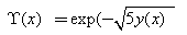
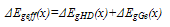
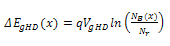
- Heterojunction Bipolar Transistor (HBT) is the outcome of extensive research on Bipolar Junction Transistor (BJT). Heterojunction Bipolar Transistor devices offer a number of advantages over their homo junction counterparts; in particular, SiGe-base HBTs are efficient alternative to III-V HBTs. Its use in very high frequency application is significant[1]. Bandgap engineering on silicon device can be done by Silicon Germanium (SiGe) HBT. Extremely high values of the emitter efficiency and additional degree of freedom in device design are possible because of a narrow-gap material in the base region. By introducing compositional grading in the base region further improvements in device performance can be achieved[2]. The Ge introduced into the base region reduces the band gap in the base, compared to that in Si BJT [3].Device characteristics of HBT are defined by two very significant parameters likeVAand β[4]. When base grading creates bandgap at the base-collector junction lower than maximum bandgap, it will increaseVAand hence βVA product which is an important Figure of merit[5]. Many works have been done to calculateVA and β.Tadao fabricated AlGaAs/GaAs/AlGaAs structure HBT and studied VA and β for this structure[6]. Tang et al. derived a closed form analytical model of VA and β for a uniform doped base HBT with very thin Si emitters[5].The effect of surface recombination of AlGaAs/GaAs/ AlGaAs HBT on the VA was studied by Chiu et al.[7]. This model did not consider the effect of electric field on mobility while calculating VA. Effect of Ge content at the collector base junction on VA was investigated by Dong et al.[8]. At high doping concentration and high Ge content, neutral baserecombination effect on β were analysed by Ningyue et al. for uniform base doping profile[9]. Prinz et al. studied VA and β in HBT where bandgap varies across the base[10]. This model is applicable for uniformly doped base and the effect of velocity saturation and field dependent diffusivity were neglected in this model. Yuan et al. modified Prinz’s works by including neutral base re-combination effect on VA[11]. Early voltage improvement using deep sub-micron technique was proposed by Conrad et al[12]. Modelling and improvement of current gain for a uniform doped base SiC power bipolar junction transistor was done by Domeij [13].A new bipolar junction transistor for enhanced current gain and reduced hot carrier degradation was proposed by Kumar et al. [14]. Ge content in the base as well as heavy base doping cause BGN[15]. So BGN due to heavy doping should consider while calculating VA and β.Zareba derived a new model of VA considering field dependent diffusivity, velocity saturation and band gap narrowing effects for Gaussian doped base HBT[16]. This model was not in closed form and it was done only for triangular germanium profile in the base.Babcock et al. have done a comprehensive investigation of temperature dependence of current gain (β) and Early voltage (VA) for SiGe-npn transistors[17]. Babcock et al. also done comprehensive investigation of Early voltage (VA) versus drive current dependence for SiGe-pnp bipolar transistors fabricated on thick-film SOI[18]. Ziao B. et al. generalized SGP model of standard Early voltage for SiGe- npnheterojunction bipolar transistors (HBTs)[19]. A complete closed form analytical model ofVA and β for HBT with different base doping profile (uniform, exponential and Gaussian) and trapezoidal/triangular/box germanium profile in the base is yet to be reported where the necessary effects were considered.In this work, a new model for Early voltage (VA) and common emitter current gain (β) were derived for three different base doping profiles (Gaussian, exponential and uniform) and Germanium profiles (trapezoidal, triangular and box). Germanium profile incorporate band gap engineering in silicon base. A model for effective intrinsic carrier concentration (nieSiGe), diffusivity (DnSiGe), electric field (ElSiGe), collector saturation current (JCO) were derived forSiGe HBT considering field dependent mobility, BGN and velocity saturation effect. These parameters were used to explain the variation of VA and β for various base doping profiles and germanium profiles.
2. Analysis
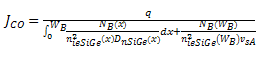
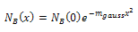
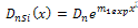
- For arbitrary doped base HBT with arbitrary Ge profile, the collector saturation current density can be expressed as [20].
 | (1a) |
 ,
,  and
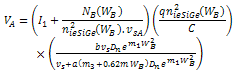
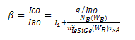
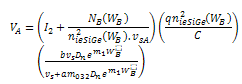
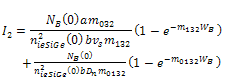
and  are the electron diffusion coefficient, effective intrinsic carrier concentration and collector saturation current density in SiGe HBT respectively. NB(x) is the base doping profile, x is the length along base, WB is the base width and vsA is the saturation velocity within the alloy, q is the charge of electron. NB(WB) and nieSiGe(WB) is doping concentration and effectiveintrinsic carrier concentration at base-collector junction respectively.The common emitter current gain (β) can be found from equation (1a)
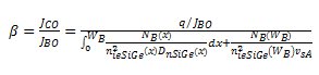 | (1b) |
 | (2a) |
 | (2b) |
 | (3) |
 | (4) |
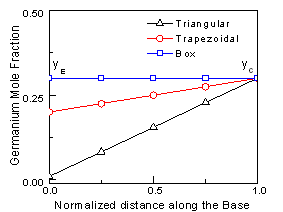 | Figure 1. Germanium profile in SiGe HBT |
 | (5) |
 | (6a) |
 | (6b) |
 | (6c) |
 | (7a) |
 | (7b) |
 | (8a) |
 | (8b) |
 | (8c) |
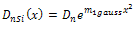
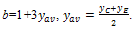
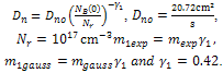 Now Electron diffusivity in the presence of Germanium is [24]
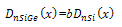 | (9) |
 The saturation velocity inside the SiGe alloy differs from that in Si and is given by[25]
 | (10a) |
 | (10b) |
 | (11a) |
 | (11b) |
 | (12) |
 | (13) |
 | (14) |
 | (15) |
 | (16) |
 | (17) |
 | (18) |
 | (19) |
 ,
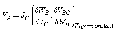
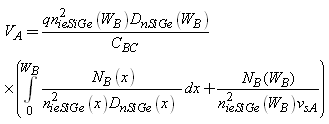
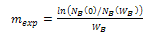
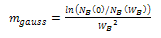
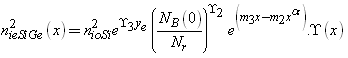
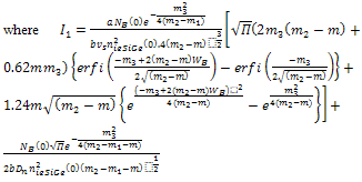
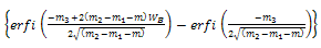
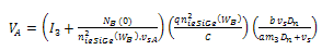
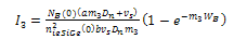
,  from equation (12), (18) and (19) respectively we can find β and VA from (1b) and (2b) respectively.Deriving the closed loop form of VA and β, ratio of effective density of states in SiGe to the effective density of states in silicon was considered fixed throughout the base region[27].
 | (20) |
 | (21) |
 | (22) |
 | (23) |
 | (24) |
 | (25) |
 | (26) |
 | (27) |
 | (28) |
 | (29) |
3. Result and Discussion
- The calculation is done for an HBT with 300Å base width. Base doping at the base emitter junction is 1019cm-3 and at base-collector junction is 1017cm-3 for Gaussian and exponential doped base and 1019cm-3 was considered for uniform doped base. The base-collector junction capacitance assumed CBC≈55 nF/cm2[10].
3.1. Electric Field Profile
- Figure 2a and Figure 2b shows that the electric field increases with yC. Figure 2a shows electric field at base emitter junction and Figure 2b shows electric field at base collector junction. Increased Germanium will enhance BGN (ΔEgeff) which will increase effective intrinsic carrier concentration (nieSiGe) exponentially (Figure 4). From equation (5) it can be observed that electric field reduces with the amount of base doping concentration and intrinsic carrier concentration but it increases with the variation of base doping concentration and intrinsic carrier concentration variation. For uniformly doped base, doping concentration made 100 times than that of exponential and Gaussian doped base in this analysis, also intrinsic carrier concentration is much more than exponential and Gaussian base (Figure 3). But due to no variation of doping concentration and intrinsic concentration for uniform doped base electric field is lowest in comparison to exponential and Gaussian doped base at collector end. On the other hand at emitter end, base doping concentration (NB) and nieSiGe are same for all types of profile but variation of base doping is much more for exponential doped base in comparison to other two profiles, so electric field is much higher for exponential doped base.
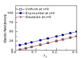 | Figure 2a. Electric field at base-emitter junction, ElSiGe(0) for yE=0.01 and varying yC for three types of doping profiles |
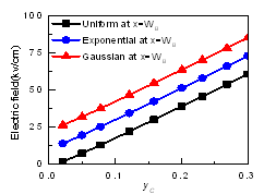 | Figure 2b. Electric field at base-collector junction, ElSiGe(WB) yE=0.01 and varying yC for three types of doping profiles |
3.2. Effective Intrinsic Carrier Concentration Profile
- Figure 3a and Figure 3b shows distribution of effective intrinsic carrier concentration (nieSiGe) throughout the base region for uniform, exponential and Gaussian doped profile. This distribution was plotted for two yC value, one for yC=0.01(Figure 3a) and other for yC=0.3(Figure 3b). In both cases,yEremain 0.01. For yC=0.01, it is observed that nieSiGeprofile exactly follows their respective base doping profile.From Figure 3b, it is observed that for yC=0.3, nieSiGe increases for all three types of base doping profile. The concentration of nieSiGe near the base-collector junction is highest for uniformly doped base. Though the concentration of nieSiGeis same at base-collector and base-emitter junction for exponential and Gaussian doped base but it is not same between these two junctions. Actually nieSiGeis proportional to base doping concentration and germanium content in the base.
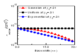 | Figure 3a. Intrinsic carrier concentration through the base for uniform, exponential and Gaussian doped basefor both yCand yE at 0.01 |
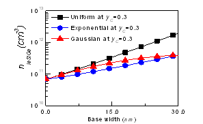 | Figure 3b. Intrinsic carrier concentration through the base for uniform, exponential and Gaussian doped basefor yC=0.3 and yE=0.01 |
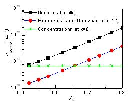 | Figure 4. Effective intrinsic carrier concentration (nieSiGe) at base-collector junction, nleSiGe(WB) and base-emitter junction, nleSiGe(0) for yE=0.01 and varying yC for three types of doping profiles. nieSiGeat x=0 is same for three profiles |
3.3. Diffusivity Profile
- Figure 5 shows diffusivity for three base doping profiles at base-collector junction. Here yEis fixed at 0.01 and ycis varied. Diffusivity is observed by both considering and ignoring velocity saturation effect.For uniform doped base diffusivity has no significant changes while variation of yC. Velocity saturation also has no significant effect on diffusivity for uniform profile. For exponentially doped base diffusivity decreases sharply with yC. Velocity saturation effect is also greater for exponential doped base and no significant effect observed for Gaussian doped base. Due to increasing electric field with yC at base collector junction and velocity saturation effect, electron mobility reduces in the base collector junction, as well as diffusivity reduces.
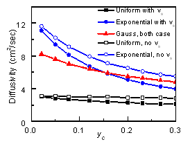 | Figure 5. Diffusion coefficient at base-collector junction,DnSiGe(WB)for both considering velocity saturation effect and ignoring that for yE=0.01 and varying yC for three types of doping profiles |
3.4. Early Voltage
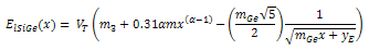
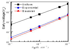
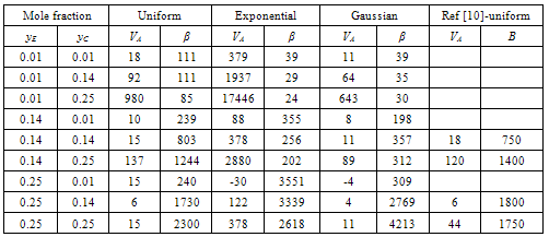
- Fig. 6 shows Early voltage for fixed yE(=.01) and varying yC. (0.01~0.3) for three types of base doping profiles. Early voltage for all three cases increases exponentially with yC.Base width, WB is 300Å, peak doping at base-emitter junction is 1019 cm-3and minimum doping at base-collector junction is 1017 cm-3 for Gaussian and exponential base profiles, 1019cm-3 considered for uniform based doping profile. VAfor uniform doped base increases almost 500 times by increasing yC from 0.01 to 0.3. For all three types of profiles VA profile is similar. According to equation (2b) if effective intrinsic carrier concentration at the base-collector junction, nieSiGe(WB) increases, it will increase Early voltage. nieSiGe(WB) for uniformly doped base is greater than Gaussian and exponentially doped base (Fig. 4), so VA for uniform doped base is greater than exponential and Gaussian doped base. It is also found that VA is greater for exponential doped base than Gaussian doped base although nieSiGe(WB) is same for both doping profiles. Actually Early voltage increases proportionally with the increase of nieSiGe(WB),but it has a inverse relation with total amount of nieSiGe content in the base (2b). Total amount of nieSiGeis greater for Gaussian than exponential doped base (Fig. 3a and Fig. 3b), and for this reason Early voltage is greater for exponentialdopingprofle than Gaussian dopingprofile.Part of our Result (Gaussian doped base) compared with[16] and found in good agreement for VA.Figure 7 shows Early voltage for varying yEwith fixed yCat 0.3. Here it is observed that by increasing yE,VA reduces exponentially for three types of base doping profiles. While yE is increased, this resulthas no variation in nieSiGe(WB), but it increases nieSiGe(0), as well asnieSiGe throughout the base region. If nieSiGe at collector end (nieSiGe(WB))is fixed but increases in the base region it will reduce VA (equation 2a). While yEis nearly 0, this profile is triangular germanium profile, VA in this profile is maximum, any other increment of yE causes VA reduces. When yE=yC=0.3, this shows box Germanium profile, in this case VA is minimum.
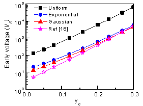 | Figure 6. Early Voltages for yE=0.01 and varying yC for Gaussian, exponential and uniform base doping profiles. Base width, WB is 300Å, peak doping at base-emitter junction is 1019 cm-3 and minimum doping at base-collector junction is 1017 cm-3 for Gaussian and exponential base profiles, 1019cm-3 considered for uniform based doping profile. Triangular symbol used for Ref [16] |
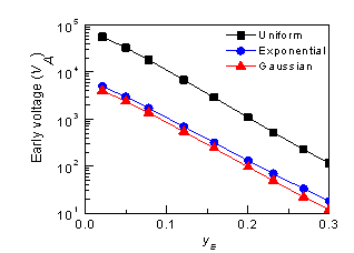 | Figure 7. Early Voltage for yC=0.3 and varying yE for Gaussian, exponential and uniform base doping profiles |
 | Figure 8. Early voltage (VA) for triangular germanium profile with yC=.3 and yE=0.01 with varying base doping concentration. Doping concentration at base-collector junction for uniform doped NB(WB)=NB(0) and for exponential and Gaussian doped NB(WB)=NB(0)/100 |
3.5. Collector Current Density (JCO) and Common Emitter Current Gain (β)
- Figure 9 shows dependence of collector saturation current density (JCO) for uniform, exponential and Gaussian doped base with varying yCand fixed yE at 0.01.JCO is considered for two cases, one is considering velocity saturation effect (vs) and another is ignoring that effect.For uniform doped base JCO decreases with the increases of yC. This decreasing of JCO is true for both cases, either considering vsor ignoring it. For exponential doped baseifvSis consideredJCO decreases, but otherwise it increases with yC. It can be explained that for exponential doped base electron velocity reaches it’s saturation value before reaching base-collector junction. If we avoid vSin our calculation, theoretically its velocity increase as well as JCO also increases but if vSis considered than electron velocity cannot overcome vS and JCO decreases. For Gaussian doped base vShas no real impact on JCO.Collector current depends on quantity of intrinsic carrier concentration (nieSiGe)as well as gradient of intrinsic carrier concentration (ΔnieSiGe) and diffusivity. The value ofnieSiGe(0) and nieSiGe(WB) for exponential doped base is same asnieSiGe(0) and nieSiGe(WB) for Gaussian doped base respectively, but total amount of nieSiGethroughout the base is not same for these two profiles (Fig. 3a and Fig. 3b). The amount ofnieSiGeis greater for Gaussian doped base, so JCO is greater for Gaussian doped base than exponential doped base.Electron mobility decreases when electric field increases (Fig. 5). Electric field increases exponentially as yCincreases (Fig. 2a and Fig. 2b) and electric field is maximum at the base-collector junction. As electric field for Gaussian doped base is higher than exponential doped base near base collector junction (Fig. 2b), so mobility for Gaussian doped base reduces at that junction as a result it cannot reach saturation value. For that reason vs makes no real difference in JCO for Gaussian doped base, but it has significant impact for uniform and exponential doped base.
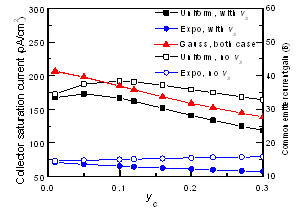 | Figure 9. Collector saturation current density (Jco) for fixed yE(0.01) and varying yC. Right side of figure shows common emitter current gain (β) considering JBO= 5pA/cm2 |
|
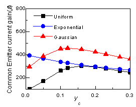 | Figure 10. Common emitter current gain (β) for yE =0.15 and varying yC for uniform, exponential and Gaussian doped base. JBO is considered 5 pA/cm2 |
4. Conclusions
- In this work, an analytical model for Early voltage (VA) and common emitter current gain (β) of Heterojunction Bipolar Transistor has been developed considering field dependent mobility, doping dependent mobility, band gap narrowing and velocity saturation effects. Dependences of Early voltage and common emitter current gain on different device parameter were studied. The results of the proposed models are compared with the data available in the literature found in good agreement. This analysis is important for optimum slection of various parameters for Early voltage and Common Emitter Current Gain of Heterojunction Bipolar Transistor.
ACKNOWLEDGEMENTS
- Authors of this paper would like to thank the Department of Electrical and Electronic Engineering (EEE), Bangladesh University of Engineering and Technology (BUET), Dhaka-1000,Bangladesh, for its various supports during the course of this work.