| [1] | Marc R.M. (2021). Transparent Ceramics: Materials, Processing, Properties and Applications; Encyclopedia of Materials; Technical Ceramics and Glasses, 1:399-423. |
| [2] | Hadjadj A., and Gilliot M. (2023). Recent Advances in Functional Transparent Semiconductor Films and coatings; Coating, 13: 307. |
| [3] | Pasquarelli R.M., Ginley D.S., and O’Hayre R. (2011). Solution Processing of transparent conductors: from flask to film; Chemical Society Reviews, 40: 5406. |
| [4] | Tyagi M., Tomar M., and Gupta V. (2013). P-N Junction of NiO Thin Film for Photonic Devices. IEEE Electron Device Letters, 34(1): 81-83. |
| [5] | Jaehoon, P. (2018). Solution-Processed Gallium-Tin-Based oxide Semi-conductors for Thin Film Transistors; Materials, 11(1): 3390. |
| [6] | Mageto J., Mwamburi M., and Muramba W. (2012). The influence of Al doping on optical, electrical and structural properties of transparent and conducting SnO2:Al thin films prepared by spray pyrolysis technique. Elixir Chemical Physics, 53(2012): 11922-11927. |
| [7] | Vikash K.R., Ganesh B.M., and Angshuman N. (2016). Band Edge Energies and Excitonic Transition Probabiities of Colloidal CsPbX3 Perovskite Nanocrystals; ACS Energy Letter, 1-20. |
| [8] | Benjamin A.D., John B., Jennilee B., Simon A., Robert G., and David O. (2017). Engineering Valenve Band Dispersion for High Mobility p-type Semiconductors; Chemistry of Materials, 29(6): 2402-2413. |
| [9] | Hosono H., Hiramatsu H., Kamiya T., Tohei T., Ikenaga E., Mizoguchi T., Ikuhara Y., and Kobayashi K. (2010). Origins of hole doping and relevant optoelectronic properties of wide gap p-type semiconductor. Journal of the American Chemical Society, 132: 60-67. |
| [10] | Kelvin Z., Kai X., Mark G., and Russel E. (2016). P-type transparent conducting oxides. Journal of Physics Condensed Matter, 28(38): 383002. |
| [11] | Liu X., Zhang N., Tang B., Li M., Zhang Y., Yu G., and Gong H. (2018). Highly Stable New Organic–Inorganic Hybrid 3D Perovskite CH3NH3PdI3 and 2D Perovskite (CH3NH3)3Pd2I7: DFT Analysis, Synthesis, Structure, Transition Behavior and Physical Properties. Journal of Physics and Chemistry Letters, 9(19): 5862–5872. |
| [12] | Sathyamoorthy R., Abhirami M., Gokul B., Gautam S., Chae K., and Asokan K. (2014). Fabrication of p-n junction diode using SnO/SnO2 thin films and its device characteristics. Electron Materials Letters, 10: 743-747. |
| [13] | Fumiyasu O., and Yu K. (2018). Design and exploration of semiconductors from first principles: A review of recent advances; Applied Physics Express, 11:6. |
| [14] | Kanghoon Y., Yong Y., Miso L., Dongsun Y., Joohee L., Sung H., and Seungwu H.( 2018). Computational Discovery of p-type transparent oxide semicondutors using hydrogen descriptor; Computational Materials, 17:4. |
| [15] | Hosono H. (2007). Recent progress in transparent oxide semiconductors: Materials and device application; Thin Solid Films, 515:6000-6014. |
| [16] | Robertson J., and Falabretti B. (2011). Electronic Structure of Transparent Conducting Oxides. In book: Handbook of Transparent Conductor. Springer, 2: 27-50. |
| [17] | Batzill M., and Diebold U. (2005). The surface and materials science of tin oxide; Progress in Surface Science, 79: 47-154. |
| [18] | Dolbec R., Khakani M.A., Serventi A.M., Trudeau R.G., and Saint R.G. (2002). Microstructure and physical properties of nanostructured tin oxide thin films grown by means of pulsed laser deposition; Thin Solid Films, 419:230-236. |
| [19] | Galatsisi K., Cukrov L., Wlodarski P., McCormick K., Kalantar-zadeh E., Cominic G.(2003). P- and n-type Fe-doped SnO2 gas sensors fabricated by the Mechano-chemical processing technique; Sensors and Actuators B; Chemical, 93:532-565. |
| [20] | Teh J.J., Ting S.L., Leong K.C.., Li J., and Chen P. (2013). Gallium-Doped Tin Oxide Nano-Cuboids for Improved Dye Sensitized Solar Cell; ACS Applied Materials and Interfaces, 5(21): 11377-11382. |
| [21] | Hsu C.L., Lu Y.C. (2012). Fabrication of a Transparent Ultraviolet Detector by using n-type Ga2O3 and p-type Ga-doped SnO2 core-shell nanowires; Journal of Nanoscale, 4: 5710. |
| [22] | Hong H.G., Song J.O., Na H., Kim K.K., Kim H., and Seong T.Y. (2007). Formation of Sb-Doped SnO2 p-type Ohmic Contact from near-UV GaN-Based LEDs by a CIO Interlayer; Electrochemical and Solid State Letters, 10: H254. |
| [23] | Presley R.E., Munsee C.L., Park C.-H., Hong D., Wager J.F., and Keszler D.A. (2004). Tin Oxide Transparent Thin-Film Transistors; Journal of Physics D: Applied Physics, 37; 2810-2813. |
| [24] | Chien-Yie Tsay, Chun-Wei Wu, Chien-Ming Lei, Fan-Shiong Chen and Chung-Kwei Lin (2010). Microstructural and Optical properties of Ga-doped ZnO Semiconductor Thin Films prepared by Sol-gel Process; Thin Solid Films. 519: 1516-1520. |
| [25] | Du J., and Ji Z.G. (2007). Effect of 1-Family Element Doping on Electronic Structures and Electrical Characteristics of SnO2; Acta Physica Sinica, 56: 2388-2392. |
| [26] | Singh A.K., Janotti A., Scheffler M., and Van de Walle C.G. (2008). Sources of Electrical Conductivity in SnO2; Physical Review Letters, 101: 055502. |
| [27] | Lee S.Y., and Park B.O. (2006). Structural, Electrical and Optical Characteristics of SnO2:Sb thin Films by Ultrasonic Spray Pyrolysis; Thin Solid Films, 510:154-158. |
| [28] | Lu Y., Wangn P., Zhang C.W., Feng X.Y., Jiang L., and Zhang G.L. (2011). First-principle on the Electronic and Optical properties of Mn-doped SnO2; Physica B: Condensed Matter, 406: 3137-3141. |
| [29] | Kumar V., Govind A., and Nagarajan R. (2011). Optical and Photocatalytic Properties of Heavily F-Doped SnO2 Nanocrystals by a Novel Single-Source Precursor Approach; Journal of Inorganic Chemical society, 50:5637. |
| [30] | Huang Y. Ji Z. and Chen C. (2007). Preparation and Characterization of p-type transparent conducting tin-gallium oxide films; Applied Surface Science, 253:4819-4822. |
| [31] | Bagheri-Mohagheghi M.M., Shahtahamsebi N., Alinejad M.R., Youssefi A., and Shokoon-Saremi M. (2009). Fe-doped SnO2 transparent semi-conducting thin films deposited by spray pyrolysis technique: Thermoelectric and P-type conductivity properties; Solid State Sciences, 11:233-239. |
| [32] | Kong J. (2007). Synthesis and properties of pure and antimony-doped tin dioxide thin films fabricated by sol-gel technique on silicon wafer. Materials Chemistry and Physics, 114(2): 854-859. |
| [33] | Jia T., Wang W., Long F., Fu Z., Wang H., and Zhang Q. (2009). Synthesis, Characterization, and Photocatalytic Activity of Zn-Doped SnO2 Hierarchical Architectures Assembled by Nanocones; Journal of Physical Chemical society, 113:9071. |
| [34] | Esro M., Georgakopoulos H., Lu H., Vourlias G., Krier A., Milne W.I., Gillin W.R., and Adamopoulos G. (2016). Solution Processed SnO2:Sb Transparent Conductive Oxide as alternative to indium tin oxide for applications in organic light emitting diodes; Journal of Material Chemical Society, 4:3563-3570. |
| [35] | Jago T., Eva G.B., Rocio O., Oihane H., Lucia M., and Javier B. (2021). Indium Tin Oxide Thin Films Deposition by Magnetron Sputtering at Room Temperature for the Manufacturing of Efficient Transparent Heaters; Coatings, 11(1):92. |
| [36] | Jabbar H.K., Selma M.H., and Fadheela H.O. (2015). Preparation and Characterization of Tin Oxide Thin Films by Using spray pyrolysis Technique; Engineering and Technology Journal, 33(3B). |
| [37] | Sapna D.P., Benjamin A.D., Sanjayan S., David O.S., Ivan P.P., and Claire J.C. ( 2018). Enhanced Electrical Properties of Antimony doped tin oxide thin films deposited via aerosol assisted chemical vapour deposition; Journal of Materials Chemistry. |
| [38] | Jain P., Singh S., Siddqui A.M., and Srivastava A.K. (2012). Tin Oxide Thin Films Prepared by Thermal Evaporation Technique Under Different Vacuum Conditions; Advanced Science, Engineering and Medicine, 4:230-236(7). |
| [39] | Jadhav H., Suryawanshi M.A., and Sinha S. (2017). Pulsed Laser Deposition of tin oxide thin films for emission studies; Applied Surface Science, 419:764-769. |
| [40] | Aravin P.P., Mohanapriya V. Dana K., Jiri M. (2020). Progress in Sol-gel Technology for the Coatings of fabrics; Material- Academic Open Access Publishing, 13(8): 1838. |
| [41] | Anna L., Alessandon C. and Maurizio F. (2017). Active Sol-Gel Materials, Fluorescence spectra, and Lifetimes; In: Klein L., Aparicio M., Jitianu A. (eds) Handbook of Sol-Gel Science and Technology, 1:1-43. |
| [42] | Exarhos G. (2007). Discovery-based design of Transparent Conducting Oxide Films; Materials Science Thin Solid Films, 515(18): 7025-7052. |
| [43] | Fredric S. (2018). Sol-Gel Technologies for Glass producers and users: Cleaning glass substrates. Sprinker, 3293: 19-34. |
| [44] | Soraya H., Saeed R., and Suraya A. (2015). Grafting Carbon Nanotubes on Glass fiber by Dip-Coating Technique to enhance Tensile and Interfacial Shear Strength; Journal of Nanomaterials, 2015(7): 1497360. |
| [45] | Abduladheem J., Supat C., Mohammed A., and Iman H. (2021). Nanomaterial by Sol-Gel Method: Synthesis and Application. Advances in Materials Science and Engineering, 21(2021): Article ID 5102014. |
| [46] | Anna L., Alessandon C. and Maurizio F. (2017). Active Sol-Gel Materials, Fluorescence spectra, and Lifetimes. In: Klein L., Aparicio M., Jitianu A. (eds) Handbook of Sol-Gel Science and Technology, 1:1-43. |
| [47] | Ramarajan R., Kovendhan M., Thangaraju K., Paul D., Ramesh R., Viswanathan E. (2020). Enhanced Optical transparency and Electrical conductivity of Ba and Sb-co-doped SnO2 thin films; Journal of Alloys and Compounds, 153709. |
| [48] | Peddavarapu S., Harish S.A., Ranjeth T., Srinvas G., Nagaiah K., Nanda N. (2021).Influence of Ga doping on Structural, Optical and Electrical properties of Transparent Conducting SnO2 Thin Films; Optik, 226:165859. |
| [49] | Goswami A. (1996). Thin Film Fundamental; New Age International (P) Limited Publishers- New Delhi. |
| [50] | Xuan P., Feng J., Jin M., Ti Ning, Zhenguo S., Yongliang T., and Caina L. (2010). Structural and photoluminescence properties of SnO2:Ga films deposited on Al2O3(0001) by MOCVD; Journal of Luminescence, 130:1189-1193. |
| [51] | Benamar E., Rami M., Messaoudi C., Sayah D., and Ennaoui A. (1999). Structural, Optical and Electrical properties of Indium tin oxide thin films prepared by spray pyrolysis; Solar Energy Materials and Solar Cells, 56:125-139. |
| [52] | Thirumoorthi M., and Thomas J. (2016). Structural, Optical and Electrical properties of Indium tin oxide ultra-thin films prepared by jet nebulizer pray pyrolysis technique; Journal of Asian Ceramic Societies, 4:124-132. |
| [53] | Vidhya S.N, Balasundaram O.N., and Chandramohan M. (2016). Structural and Optical Investigations of gallium doped tin films prepared by spray pyrolysis; Journal of Saudi Chemical Society, 20: 703-710. |
| [54] | Nripasree N., Deepak NK. (2018). Ga Dopant Induced Band gap Broadening Conductivity enhancement in spray pyrolysed Zn0.85Ca0.15O thin films; Materials Research, 21(6). |
| [55] | Burstein E. (1954). Anamolous Optical Absorption limit in InSb; Physical Review, Crystal Branch, Metallurgy Division, Naval Research Laboratory, Washngton, D, 93: 632-633. |
| [56] | Cao P., Thi A., Dong K., Wen K., Thach N. (2020). Reactively Sputtered Sb-GaN Films and its Hetero-Junction Diode; The Exploration of the n-to-p Transition, 10(3):210. |
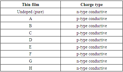
| [57] | Paul D., Devarajan U., Jean F., Ramarajam M., Korendhan M., Nandarapu P., Reddivari M., Venkatenswan C. (2021). Lithium-antimony co-doping induced Morphology transition in spray deposited SnO2 thin films; Surfaces and Interfaces, 23: 100918. |

 Abstract
 Reference
 Full-Text PDF
 Full-text HTML

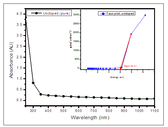
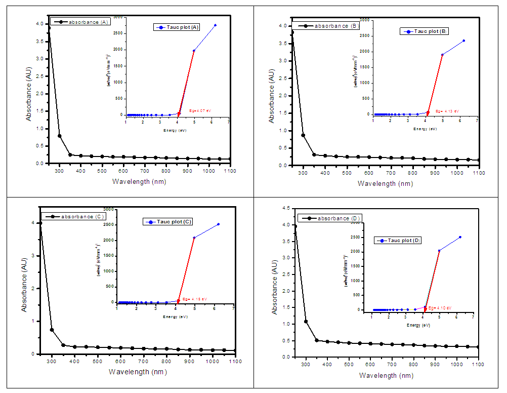
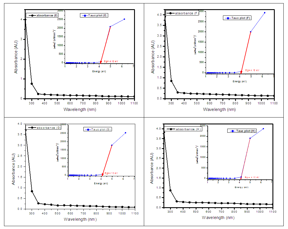
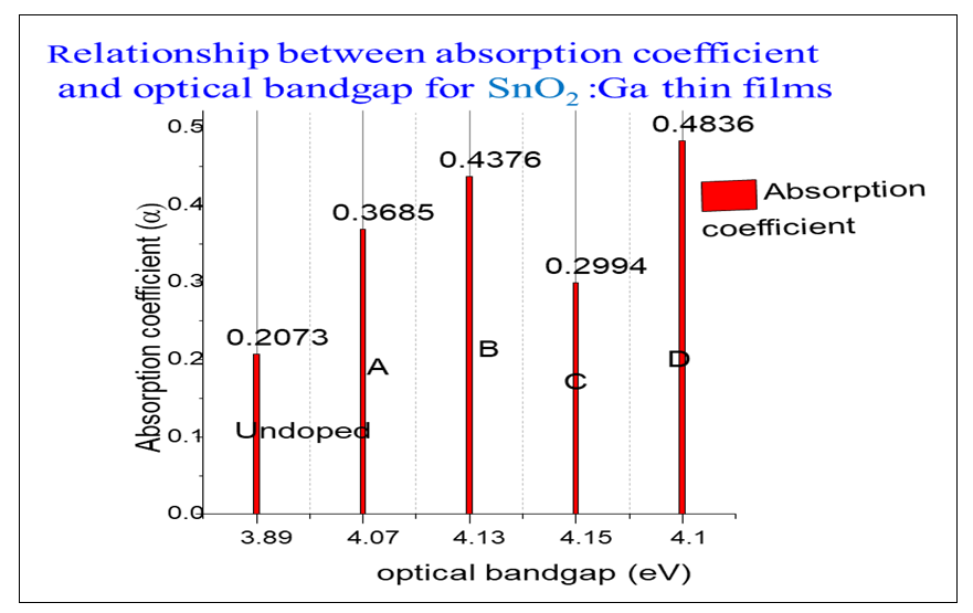
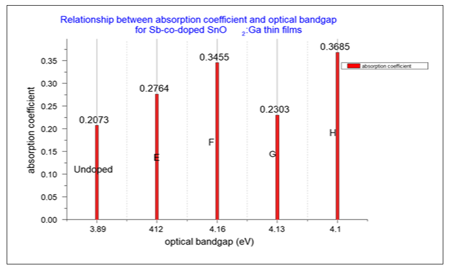
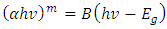 Where B is a constant and Eg is the optical bandgap [49], [50].The band gaps were computed from the extrapolation of
  versus
  curves to the x-axis as shown in Figure 6, Figure 7 and Figure 8.