-
Paper Information
- Paper Submission
-
Journal Information
- About This Journal
- Editorial Board
- Current Issue
- Archive
- Author Guidelines
- Contact Us
American Journal of Materials Science
p-ISSN: 2162-9382 e-ISSN: 2162-8424
2021; 11(1): 20-35
doi:10.5923/j.materials.20211101.03
Received: May 8, 2021; Accepted: Jun. 2, 2021; Published: Jun. 15, 2021

Nickel-Based Inks for Inkjet Printing: A Review on Latest Trends
 Abstract
 Reference
 Full-Text PDF
 Full-text HTML
Neha Thakur, Hari Murthy
Department of Electronics and Communication, CHRIST (Deemed to be University), Bengaluru, Karnataka, India
Correspondence to: Neha Thakur, Department of Electronics and Communication, CHRIST (Deemed to be University), Bengaluru, Karnataka, India.
| Email: |  |
Copyright © 2021 The Author(s). Published by Scientific & Academic Publishing.
This work is licensed under the Creative Commons Attribution International License (CC BY).
http://creativecommons.org/licenses/by/4.0/

Currently, inkjet printed conductive films have attracted more and more attention in the field of electronic devices. Metallic nanoparticles are the most popular choice for the fabrication of conductive ink because of their low melting point and high electrical conductivity. Gold (Au) and silver (Ag) nanoparticles (NPs) are the most commonly used materials for synthesizing conductive inks due to their high conductivity and anti-oxidation properties but suffer from the high cost of manufacturing (because of nanoparticle synthesis) which hinders their practical application. These also suffer from electromigration which lowers reliability. In this review paper, conductive nickel inks are reviewed along with their composites like copper, silver, graphene, and other composites. The reason for choosing nickel-based ink is because of its excellent conductive properties while being more economical. Particle size, film thickness, and electrical resistivity of the inks are compared for various ink compositions. This review paper comprises the research done on nickel conductive inks for various printing and coating techniques from 1983 to 2021. An extensive literature survey is done for nickel-oxide and nickel-metal inks. Metals considered in the research are silver, copper, graphene, Yttria-stabilized zirconia (YSZ), manganese, and lithium. The highest conductivity obtained for nickel used with multi-layered graphene (MLG) sheet is 400S/cm. A wide range of temperature (room temperature to 1600°C) usage is observed for various nickel-based inks. The smallest particle size observed is 1nm for nickel-based conductive ink. Various techniques like spin coating, 3D printing, screen printing, spray coating, electrodeposition technique, chemical vapor deposition, polyol process, hydrothermal process, transmelation process, inkjet printing techniques have been used in literature. Out of all the techniques, inkjet printing technique has shown the best result in terms of resolution, line width, and conductivity.
Keywords: Inkjet Printing, Conductive ink, Nickel ink, Particle-free ink, Particle-based ink, Nickel-silver ink, Nickel-copper ink, Nickel-graphene ink
Cite this paper: Neha Thakur, Hari Murthy, Nickel-Based Inks for Inkjet Printing: A Review on Latest Trends, American Journal of Materials Science, Vol. 11 No. 1, 2021, pp. 20-35. doi: 10.5923/j.materials.20211101.03.
Article Outline
1. Introduction
1.1. Inkjet Printing
- Conventional deposition techniques like vapor deposition, photolithography, electroplating, polyol process, etc. require a very intense setup with stringent operating conditions. For vapor deposition techniques a clean room setup is required. Photolithography requires hazardous chemicals as photoresists (positive or negative). Electroplating needs a complex setup including electrodes, bath, electrolyte, etc. The polyol process requires a high temperature. On the other hand, liquid precursor deposition methods are available which require simple design and inexpensive equipment, scalability, and do not require any sophisticated infrastructure. There are deposition methods available, including spin coating, spray coating, 3D printing, and inkjet printing. Inkjet printing (IJP) is a digital printing technique, a derivative of direct-write (DW) processing, offers numerous advantages including low material wastage, non-contact processing, and the elimination of photolithography [1]. Recent advances in the field of inkjet printing have shifted the focus to the development of conductive inks for applications in flexible electronics. This conductive material can be used for the fabrication of printed circuit boards (PCBs), thin-film transistors (TFT), RFID tags, photovoltaic (PV), transparent conductive electrodes, touch screens, flexible displays, and electrochromic devices [2]. Inkjet printers are capable of line resolution < 20µm, which is two to four times better than the current method of screen printing. Screen printing although is used in many applications, is not economical for expensive nanoinks. The typical thicknesses of the conductors are 5 to 10µm which is not economical due to the high cost of screen printing. The essential requirements for the printed film are accuracy, high resolution, high electrical, and thermal conductivity, thickness, and longevity. The printed layer should be free from the following defects (i) Ink Overflow– Refers to widening of the printed tracks, (ii) Surface Roughness-Refers to discontinuities and irregularities in the surface, (iii) Jagged Edge and Discontinuity- Non-uniform edges lead to shorting of adjacent tracks [3]. Figure 1 represents the main components of the inkjet printing process and their properties.
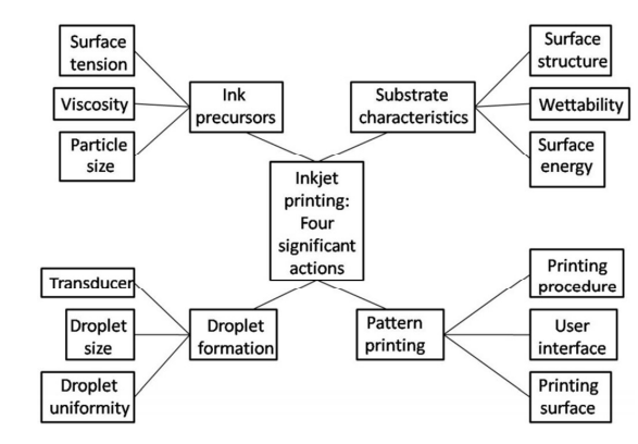 | Figure 1. Inkjet printing main components and properties [4] |
1.2. Inks
- The two major components of printer ink are the precursor and an organic solvent. The precursor is the compound that decomposes into the desired material or metal along with various additives (surface tension modifiers, defoamers, binders, and humectants). The application of metallic NPs-based inks in the fabrication of electronic devices require optimization of their properties such as the wetting and spreading to obtain the efficient matching of ink to the substrate surface. The particle size should be one-tenth of the printhead’s nozzle diameter to avoid nozzle-clogging and blockage of the printhead. The particle size also influences the melting temperature and resistivity. The conductivity of the nanocomposite materials can be improved by using heterogeneous nanoparticles. Viscosity and wettability of the conductive ink affect the quality of the coating. Wetting which determines the amount of drop that spreads out on a substrate is also critical [9]. A number of factors affect the conductivity of the films such as metal loading, number of printed layers, post-printing treatment. High metal loading increases the conductivity but only when direct contact between the metal NPs within the ink layer and substrate is present. The contact is prevented due to the presence of organic stabilizers on the NP surface resulting in low electrical conductivity. Thus, post ink coating, sintering is required to remove the organic layer improving the metal NPs-substrate contact. Various sintering techniques have been investigated including heat, intense light pulse, microwave radiation, plasma, high electrical field, and chemical sintering agents, with thermal sintering the most commonly used approach. The efficiency of thermal sintering depends on the nanoparticles’ size, the decomposition temperature of the organic compounds of the ink, and boiling point of the ink solvent. During thermal sintering, thermal decomposition and evaporation of organic additives lead to the formation of necks and inter-particle connections. The metallic film develops due to inter-particle atomic diffusion is driven by the reduction of surface energy [10]. Figure 2 represents a brief overview of the printing and curing process in the inkjet printer.
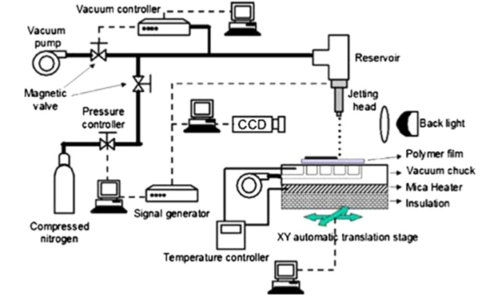 | Figure 2. Schematic overview of printing and curing process [11] |
1.3. Conductive Inks
- Conductive inks have received tremendous attention in today’s electronic era. There are two types of conductive inks, particle-based ink and particle-free inks. Particle-based inks or nanoinks utilize nano-particles as the main component. Nanoparticle synthesis is a tedious process that includes high-speed centrifugation, multiple washing steps, high vacuum drying, and high-temperature annealing, thereby making the processing time-consuming and costly. Particle-free ink (MOD ink or precursor ink or reactive ink) is composed of metal salts or metal complexes as precursors dissolved in suitable solvents, and offers high flexibility in preparation, with excellent stability and lower sintering temperature (<200°C) than nanoinks [6]. The inks are deposited on various substrates like plastic [12], paper [13], glass [14], PET [12], etc. using techniques such as spin coating [15], screen printing [16], roll to roll (R2R) process [17], and inkjet printing [18] technique, etc. Inkjet printing technology offers various advantages of maskless, non-contact, low-cost methods with high material utilization over other technologies. Drawbacks of inkjet printing are particle agglomeration and coffee ring effect. Particle agglomeration does not occur in particle-free inks as nanoparticles are not suspended into it as shown in Figure 3.
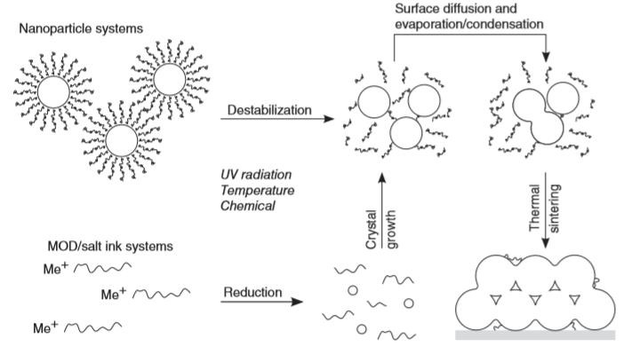 | Figure 3. Ink formulation process for conductive inks [19] |
1.3.1. Nickel Oxide Nanoink
- In this section, nickel particle-based inks are discussed using Nickel oxide (NiO) as the precursor. Wide range of additives, solvents (α-terpineol/butyl carbitol acetate [30], oligomer polyester [31]), binders (EC) [30] [29], and substrates (Mylar [32], stainless steel [33]), are used for depositing the conductive film from μm to nm range. Different techniques such as Polyol [34], IJP [35] [36], spin coating [37] [38] [39], screen printing [40], FACVD [41], APPJ [42] etc. can be used for various applications such as RTD [43] [16], OLED [39] [44], PSC [41] [45] [46] [47], supercapacitors [34] using NiO conductive ink.In 1983 Kondo et al. [27] opened the gateway for formulating conductive inks using nickel. The ceramic metalizing ink for low resistance conductors or wire in order to prevent overheating was developed. The metal powder (1.33μm) component comprising tungsten, molybdenum, or a combination of both was used at 1600°C. The obtained resistivity was 10.5μΩ.cm to 15.2μΩ.cm. Morgan et al. [32] formulated a low temperature (<200°C) solventless, screen printable, heat curable, conductive ink for fabricating resistors or conductors on substrates to form circuit boards and electronic membrane keyboards. The ink also has good adhesion to the substrate, flexible, electrically conductive, fast curing (<30 minutes), good shelf life. When nickel powder is screen printed in a line circuit pattern through a 165 mesh stainless steel screen onto a Mylar substrate at 160°C for 10 minutes then high resistivity 0.014 Ω.cm was obtained. The estimation of the dispersion behavior process of the ink remained unknown. Hsu et al. [30] investigated the dispersion behavior of NiO–CuO–ZnO ferrite powder in an α-terpineol/butyl carbitol acetate (BCA) with ethylcellulose (EC) binder. Rheological results show that a dispersant of phosphate ester can effectively disperse low-fire ferrite powder in the above organic solution. The organic vehicle of 15 wt.% EC T-45, 8 wt.% TCP, and 77 wt.% of 25 vol.% BCA/75 vol.% α-terpineol is formulated for low-fire NiO–CuO–ZnO ferrite paste. As the molecular weight of EC increases viscosity also increases. The viscosity should be in the range of 30,000–50,000cP, for the paste which was obtained by T-45 and N-7. Complex binders like BCA can be avoided. Tseng et al. [31] used easily available solvents like α-terpineol for dissolving NiNPs for observing rheological behavior and suspension structure using different organic surfactants with varying concentrations (0–10 wt.% of the powder) and solids loadings (φ=0.01–0.28 in volumetric ratios) over a shear-rate range 10–103s−1. Oligomer polyester surfactant was found most effective at concentrations 2–4 wt. % of the solids. Viscosity increases rapidly when the concentration of surfactant goes beyond 2–4 wt. %. With the increase in shear rate, pseudoplastic flow behavior was found, and a maximum solid concentration (φm) of 0.32 was observed. Reaction-limited cluster aggregation (RLCA) with fractal dimension (Df) of 2.0 was calculated for inter-particle potential. Even after the addition of surfactant, the NP inks were agglomerated in the character. In order to overcome the problem of ink agglomeration, Kamikoriyama et al. [29] dispersed NiNPs from nickel slurry as dispersion medium which was passed through a membrane filter. The concentration of slurry was adjusted according to the requirement by the centrifugal separator. Viscosity and surface tension of the ink observed were 0.6-60mPa.s and 15-50mN/m respectively. The average surface roughness (Ra) obtained was 10 nm and the maximum surface roughness Rmax was 200nm. The IV profile was first obtained by Takami et al. [38], they synthesized NiO nanoplates (∼10nm thick and 100–500nm lateral size) by hydrothermal reaction using a flow-type reactor. The nanoplates fabricated were used as the channel material in a field-effect transistor (FET) after annealing at 300°C. NiO nanoplates worked as the p-type semiconductor according to the Id–Vd profile. For NiO nanoplates, the optical bandgap evaluated was 3.45 eV. The results are stable in air and water which makes the nanoplates suitable for various magnetic, ferromagnetic, ferroelectronics, and catalysis applications. The overall cost of the setup is very high. Kettle et al. [37] investigated one polymeric (PEDOT:PSS) and two metal oxides (NiOx, MoO3) HTLs for PCPDTBT:PCBM solar cells using RF sputtering technique. Furthermore, the stability of OPVs fabricated with a NiO layer was enhanced by removing the PEDOT: PSS HTL. Improvement in the performance was observed by the better alignment of the energy levels, increased series resistance, and electric field across the active region. For thin layers (<34nm), or PEDOT: PSS, improved performance was observed due to an increase in the modulation of the electric field within the active region at a lower cost. The total decrease in resistance was 17-27%. Manders et al. [39] used NiO films as HTL for solar cell implementation because of better fill factor and short circuit current. The PCE increased by 14.7% by using NiO instead of PEDOT:PSS because of improved optical resonance, nanoscale active layer morphology, and high shunt resistance, and low series resistance for charge extraction in the NiO devices. Liu et al. [48] used s-NiOx with hole injection efficiency of 80% and field-effect hole mobility of 0.141cm2/Vs. The maximum power efficiency of 75.5±1.8mW was obtained for phosphorescent green OLED with UV ozone treated s-NiOx HIL/HTL, which is much higher than the device with PEDOT: PSS HIL. The UV-ozone treated s-NiOx HIL/HTL was also compared with OLEDs with thermally evaporated HTL and both devices show similar performance at high luminescence intensities. Ruscello et al. [49] deve-loped NP-based NiOx HTLs for organic solar cells (~100°C). NiOx:PEO is responsible for high power efficiency, produced HTLs for P3HT:PCBM bulk heterojunction solar cells using IJP with comparable efficiencies to devices produced with high-temperature precursors. The implementation of heterojunction solar cells is very complex. Lee et al. [50] used the laser direct writing (LDW) method for direct patterning of thin (∼40 nm) Ni electrodes generated from NiO NP ink. High transmittance (>87%), was achieved for electrically conducting panels for a touch screen application. The sheet resistance of the electrode was 655Ω/square. The sheet resistance obtained is high which leads to less current-carrying capability. To improve the current- carrying capability Sung et al. [40] investigated a flashlight sintering process for NiNPs (10nm) for multilayer ceramic capacitors, magnetic devices, and printed electronics. The uniform diameter NiNPs (50nm) could not be sintered, while the NiNPs with varying diameters (5–500nm) were sintered by flashlight irradiation. For high electrical conductivity, sintering parameters such as light energy and pulsed light patterns were optimized. Also, the nickel nanoinks were optimized by changing the weight fractions of the organic binder in the ink. The resistivity obtained was 76.34μΩ.cm. Many materials used were not eco-friendly. Jakus et al. [45] developed 3D inks by mixing solvent, powder, and the biomedical elastomer, polylactic-co-glycolic acid (PLGA) for green-body structures that can be converted into sintered metallic counterparts. The printed film can have a thin, thick, high aspect ratio, hollow and enclosed, and multi-material architectures at 150mm.s–1. After printing, green bodies are transformed into metallic structures without any cracks or deformation caused because of high-temperature sintering in the H2 atmosphere. The cyclic reduction and oxidation of 3D-printed iron oxide constructs, which remain intact through numerous redox cycles verify the method. Sharma et al. [43] determined the influence of surfactants, additives, particle size (1.31nm to 22.23nm), and shape on Surface Plasmon Resonance (SPR). Effect of primary particle size, size distribution, and dielectric environments of non-ionic PVP, cationic CTAB, and anionic EDTA separately in ethanol was observed. Increasing the concentration of PVP leads to enhanced SPR intensity and shifts its position towards a higher wavelength. 1.31nm NPs with EDTA as additive yield best dispersibility and also showed superparamagnetic behavior at 300K indicating their favorable application potentials. Turkani et al. [16] fabricated Ni-based RTD on a polyimide (PI) substrate using the screen printing process from 60°C to 180°C at a constant humidity of 20%RH. The percentage change in resistance of 109% was observed from -60°C to 180°C. For RTD the linear response with a TCR of 0.45%/°C was obtained. The transient response was used to measure the repeatability of the RTD during the dynamic heating-cooling cycles. Yates et al. [41] used Flame Assisted Chemical Vapor Deposition (FACVD) process and spin coating technology for thin film deposition of polycrystalline NiO for Perovskite Solar Cell (PSC) fabrication. The maximum efficiency achieved was 12.3% for 36nm NiO HTL film. The current density increased from 16.6 mA/cm2 to 19.0 mA/cm2. Puerto et al. [35] formulated three Water: DEG-based inks; ink1 (without additives), ink2 (presence of citric acid), and ink3 (presence of urea) to prepare NiO thin films for FTO substrate using IJP. The performance of ink2 was highest because of the presence of Ni3+ surface species. Lin et al. [51] used Scanning atmospheric-pressure plasma jet (APPJ) treatment of NiO at 500°C for fabricating p-i-n structure PSCs. The post-treatment process enhanced light scattering for improved cell efficiency. Within three APPJ scans, the average PCE improves from 11.91% to 13.47%, with the best-performing PSC achieving an efficiency of 15.67%. Marques et al. [52] inkjet-printed high-performance pn-diode using NiO or CuO as p-type semiconductor oxide and Indium oxide as n-type semiconductor oxide. The current driving ability through the diode is obtained within the range of 10−11A to ∼10−4A. The emission coefficient obtained for the CuO and NiO-based pn-diodes is 1.505 and 2.199, respectively. Furthermore, a model suitable for circuit simulation is developed, for the implement-ation of PDK. The number of curing steps are involved in the process. Altar et al. [53] developed a single-step curing process for nickel inks and determined the spreading behavior of it on the Solid bleached sulphate paperboard (SBS) and polyethylene terephthalate polymer (PET) substrates. The use of porous SBS substrate reduced ink usage by 20%. With one-step photonic curing, the electrodes on SBS and PET exhibited electrical performances of a minimum of 4 Ω/sq. and 16 Ω/ sq., respectively, at a pulse length of 1.6ms, which is comparable to conventional thermal heating at 130°C for 5 min. Table 1 summarizes nickel oxide precursor inks using different technologies.
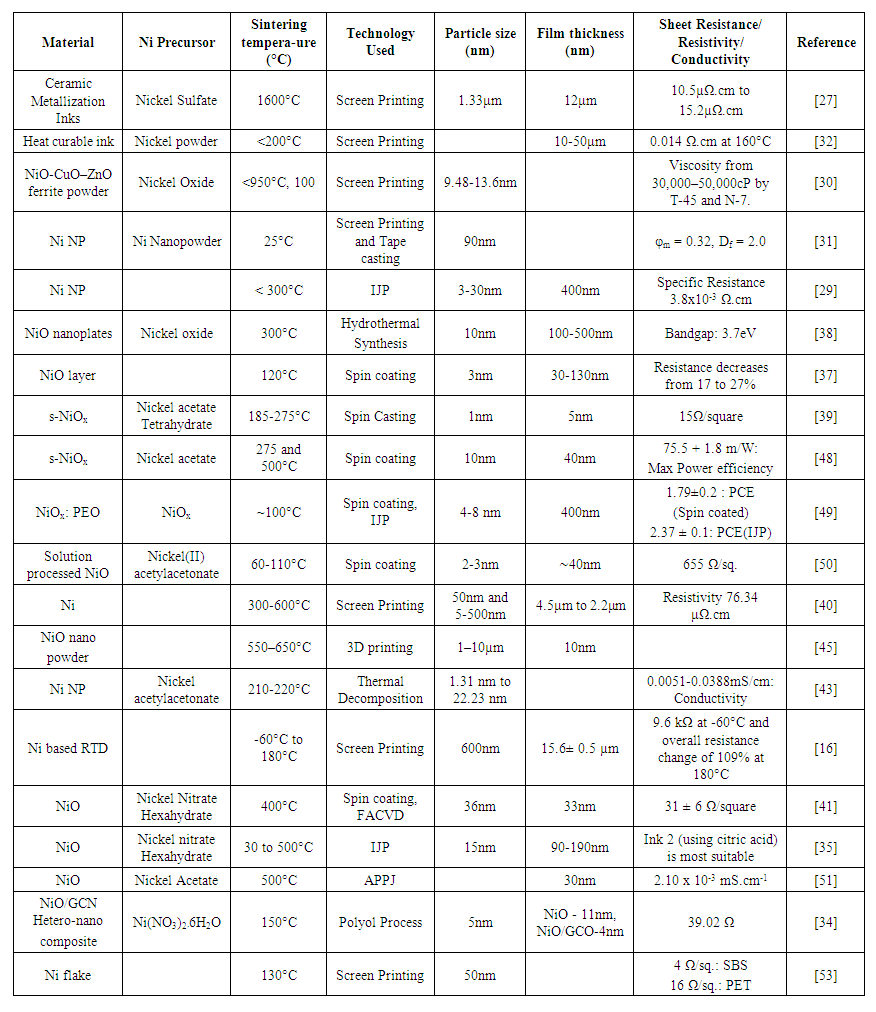 | Table 1. Nickel oxide precursor ink used for various technologies |
1.3.2. Nickel-Silver Nanoink
- Silver has advantages of low oxidation resistance and high conductivity, it also has a high cost. In order to increase the conductivity of nickel ink, silver can be used which leads to a low cost and low resistivity of 1.59x10⁻⁸ Ω.m [6]. A wide range of techniques was used for making applications based on nickel-silver nanocomposites using IJP [10] [36], Aerosol Jet [54], Screen-printing [55], HTRJ reactors [56], etc. For nickel-silver composites of nanoinks were formulated from the wide range of temperature from 25°C [10] to 800°C [55]. The particle size varied from 500µm [57] to 5nm [56]. An increase in conductivity is observed when nickel-silver composites were used. There will be an increase in manufacturing costs because of the incorporation of silver nanoparticles. Silver-based inks are known for their stability and higher conductivity than either copper or aluminum [3].Teichmann et al. [57] developed a copper (20% wt. of the sphere) coated nickel particle using a plating system. Silver is coated over copper to avoid oxidation. The thickness of the copper coating on each nickel particle is 7.8-61µm and that of silver is 300Å. An electroconductive body is developed in which the coated particles embedded in the matrix constitute at least about 15% by the weight of the matrix. The results confirm that nickel can be successfully electroplated with copper and silver for making electroconductive devices. Once the nickel- silver compatibility is confirmed then Chen et al. [58] prepared Ni–Ag core-shell NPs by colloid dispersion by using hydrazine as a reducing agent of metal salts in ethylene glycol (EG) without the addition of protective agents. Ni cores covered by Ag nanoshells whose thickness was controlled by silver nitrate concentration. To avoid particle agglomeration, the Ni concentration for the coating of Ag nanoshells size <1.0mM due to the absence of protective agents. The product obtained has the combined advantages of the surface character of Ag and the magnetic property of Ni, which makes it helpful for many potential applications. It was difficult to maintain drop spacing because of particle agglomeration. Pasquarelli et al. [36] used wet and hot print approaches for printing Ni ink. In the hot printing approach, it was found that at 30µm drop spacing the thickness of the hot print remained unaffected by the number of rows printed next to each other while in the wet printing approach thickness increases with drop spacing. Various substrates like glass, Ar coated Si, TCOs, and multi-layered metallization are used for verifying the functionality of the photovoltaic cell. The resistivity of the Ni lines decreased as the number of printed layers increased. The best resistivity of 1.7x10⁻⁴Ω.cm was obtained at 10 layers. Only straight lines with uniform spacing were printed. Jun-Jie et al. [55] used liquid-phase reduction for the preparation of Ni-Ag core-shell NPs with shells of different thicknesses around NiNPs cores with a spherical shape. The thickness of the Ag nanoshells could be varied by changing the silver loading. The surface characteristics of Ag and the electroconductive properties of Ni allow the Ni-Ag core-shell to be used for conductive pastes. At 650°C the resistivity of the core-shell is 11mΩ/square. The results verify the feasibility of using Ni-Ag core-shell for conductive pastes. Wang et al. [54] used the Aerosol Jet printing process for the fabrication of miniaturized thermistor sensors for temperature sensing applications. A circular NiO thin-film was placed in between the two parallel silver conductive tracks to form a thermistor. The thermistor operates at 30-250°C sensitively (B value of ~4310 K) without hysteretic effects. Hou et al. [47] allow low-temperature fabrication of high-quality oxide functional films from solution-based sol-gel processes, which can be used in thin-film solar cells. For the sol-gel process, a metal phase is embedded within the sol-gel precursor films for a low sintering temperature range (160-300°C). The cata- lytic Metal-induced crystallization (c-MIC) mech- anism reduced the sintering temperature of the Au-embedded NixO HTL by 100°C, making the NixO process compatible with plastic substrates. For c-MIC NixO film, the flexible PSCs achieved PCE of 15.9% and 19% for rigid PSCs at 65°C for >1200h and 65% relative humidity. Pajor-Swierzy et al. [10] used silver metallic coatings over NiNPs core shells for high electrical conductivity which depends upon temperature and the sintering process. The sheet resistance was observed for 80nm and 280nm sheets. For 80nm sheet resistance decreases up to 330°C and then increases. For 280nm sheet resistance increases only for 250°C to 330°C else it decreases. Silver core-shell prevents Ni NP even after 350°C. A characteristic peak was obtained at 853eV. A continuous layer of NP was formed at 350°C which confirms the formulation of conductive ink using nickel nanoparticles. Pajor-Swierzy et al. [7] used two methods for nickel-silver core-shell NPs. (i) Excess of NaBH4 (reducing agent) was used that was washed out later to avoid the formation of AgNPs (70nm) during the transmetalation phase. (ii) Deficiency of NaBH4 was applied, no need for washing the Ni nanocores before the formation of the Ag shell (250nm). The Ni@Ag nanoparticles show a long-term (6 months) stability which makes them suitable for conductive materials applications. It was found that at 140°C and above 180°C, Ni inks were still wet which suggested that the decomposition happened without solvent evaporation which would yield poor quality lines. At larger drop spacing (>40µm), individual drops are formed and as the drop spacing decreases, more drops and more material are required to create a line which affects the line width and thickness. The optimum temperature was thus kept at 180°C with a drop spacing of 30µm. The resistivity obtained was 11mΩ/square at 650°C. The zeta potential of the dispersion was determined to be -39mV and varied from -30mV to -45mV depending on the size of the NPs and electrostatic stabilization. When the glycerol-based solvent is used instead of water-based, the viscosity and wettability of the ink is improved. Mohammadi et al. [56] synthesized nanoinks by a one-step continuous flame-based process using High-Temperature Reducing Jet (HTRJ) reactor to produce bimetallic nickel-silver nanopowders simultaneously. Ni-Ag Functionalized-NanoPowders (FNPs) were characterized and compared with BareNanoPowders (BNPs) to verify ligand attachment. These sintering-free bimetallic conductive NPs can be used as a lower-cost replacement for current Ag inks for single-step printing of conductive traces without post-processing. Prieto et al. [59] performed the chemical state analysis and optical XRD of Ag-Ni bimetallic nanoparticles to determine the chemical structure of the NPs systems. The seed-mediated growth method is used to produce Ag, Ni, and bimetallic Ag-Ni NPs (≤35nm). For bimetallic Ag-Ni NPs, the XPS results are consistent because of the presence of a metallic Ag core surrounded by NiO+Ni(OH)2 shell. The surface plasmon resonance (SPR) peak of Ag-Ni NPs shows a blue shift from 405nm to 375 nm. Huang et al. inkjet-printed lactate sensor used for blood plasma test. Two electrodes made up of AgNPs/NiO NPs/Polyurethane (PU) and Ag/AgCl(s)/PU layers are inkjet printed. The linear sensitivity of 8.86nA/mM/mm2 was obtained in the range from 0.6 to 2.2 mM [60]. The lowest sheet resistivity obtained is 7Ω/square, which clearly indicates high current so it is suitable for high-speed applications that can be targeted if nickel and silver nanoparticles are combined together. Table 2 summarizes all the inks formed by nickel-silver composite.
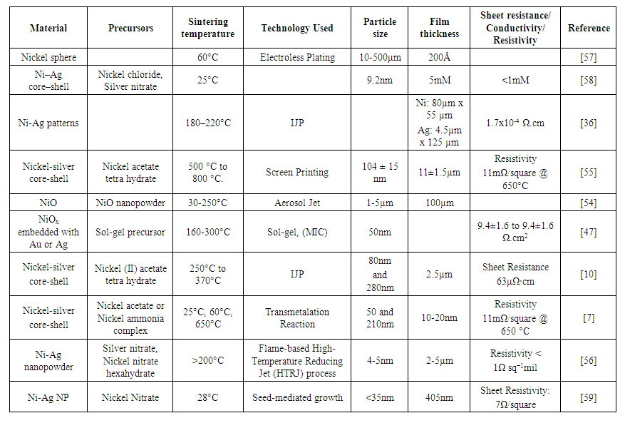 | Table 2. Nickel-silver conductive inks |
1.3.3. Nickel-Copper Nano-Ink
- Nickel-silver composite ink provides good conductivity at a high-cost. The cost can be reduced by using copper metal instead of silver. The resistivity of copper is 1.72x10⁻⁸Ω.m which is slightly less than silver. It is a ductile material with high thermal conductivity of 401W/mK [6]. Copper oxidizes quickly in ambient conditions to form a layer of non-conducting oxide reducing the printed track conductivity [3]. A wide range of nickel-copper composites are studied for the temperature ranging from 25°C [61] to 800°C [62]. The highest conductivity obtained is 1.8x10⁶S/m [28]. A variety of techniques such as microemulsion [63], electrochemical deposition [61], IJP [64], and aerosol jet printing [62] can be used for nickel-copper composite ink printing or deposition. The inks are usually available in a low-viscosity range making it difficult to use in R2R (Roll to Roll) manufacturing employing high-speed gravure printing [3].During ink composition, the main problem arises is that, in what proportion the two salts should be used. Badawy et al. [61] observed the effect of the systematic increase of Ni content (5, 10, 30, and 65 mass%) on the electrochemical behavior of the Cu–Ni alloys in neutral chloride solutions. The increase of chloride concentration up to 0.3 mol.dm−3 increases the corrosion rate. At higher concentrations ([Cl−] > 0.3 mol.dm−3) the corrosion rate decreases. The increase of Ni content along with immersion time of Cu–Ni alloys in chloride solutions improve the corrosion resistance of these alloys. The calculated sheet resistance was 53.2-8KΩ.cm-2. Ahmed et al. [63] investigated in detail about the salt proportion and synthesized Cu–Ni (1:3, 1:1, 3:1) by a microemulsion method. These bimetallic nano-particles (20-30nm) show ferromagnetic behavior and the magnetization decreases with an increase in the concentration of copper. The specific surface area of these alloy NPs was found to be in the range of 6–9.42m2/g. Li et al. [28] developed a RIJP process for printing conductive copper and nickel lines on paper. The electroless copper plating bath solution consists of copper citrate, NaBH4, reducing agent, and pH adjuster. The best conductivity of printed copper lines was 1.8x10⁶S/m (1/30 of bulk) and that of nickel was 2.2x10⁴S/m (1/600 of bulk). Edit et al. [62] prepared Cu, Ni, and Cu-Ni alloy particles using the solution combustion method. The sintering behavior of Aerosol Jet printed and sintered metal and alloy structures, as well as their microstructural and functional features (resistivity), were determined. Sinter shrinkage was observed for Cu0.8Ni0.2, Cu0.6Ni0.4, Cu0.5Ni0.5, Cu0.4Ni0.6, and Cu0.2Ni0.8 alloys from 300°C to 800°C. Well-crystallized printed layers with low resistivity of 8.67x10⁻³Ω.m were obtained after sintering at 800°C in the case of all alloys. Yabuki et al. [65] used a copper-nickel-amine complex to synthesize copper-nickel conductive films with anti-oxidation properties. Ni conductive film was prepared from a nickel-amine complex via a thermal decomposition process and deposited on a glass substrate. Nickel Formate:TETA>2 (molar ratio), to determine the optimal conditions for resistivity measurements. The resistivity of nickel film obtained was 460μΩ.cm at 230°C. The obtained film consisted of bridged NiNPs 100-200nm in size, has many voids. TETA was adsorbed onto the surface of a nickel particle, which resulted in a bridge-type connection by the nickel particles. Tomotoshi et al. [66] implemented copper-nickel electrodes for printed electronics applications on flexible polymer substrates. In order to improve the conductivity upto 10–5 Ω·cm, Ni was decorated on the Cu flakes (especially on the edge) at 150°C. The resulting Cu-Ni electrodes have shown high stability against oxidation up to approximately 400°C in air, as well as at 80°C and 80% RH after 7 days. When copper is used with nickel. Then a decrease in conductivity is observed as compared with silver. Using copper instead of silver will surely decrease the cost of the end product. Table 3 summarizes various forms of nickel and copper combined to form inks for various printing applications.
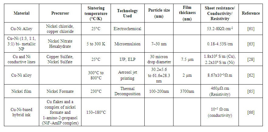 | Table 3. Nickel-copper composite ink using different printing technologies |
1.3.4. Nickel-Graphene Composite Inks
- A single layer of graphite is called “Graphene”. Graphene has high electrical conductivity due to sp2 hybridization. Graphene-based inks have opened up a new dimension in printable conductive inks [3]. Nickel-graphene is the best case of lattice-matched case. The strong chemical interaction is because of hybridization between d-electrons of Ni(1 1 1) metal and the p-orbitals of graphene. The energy band gap of nickel-graphene composite is also less and the interlayer spacing between the two materials is 0.21nm, which is the lowest amongst all the transition metals [67]. Applications like super capacitors [68], scaffolds [67], etc. are already developed using nickel-graphene composites and more are anticipated. For graphene inks, the methods used are various exfoliation methods [69] which are not environment-friendly and cost-effective. Green methods [70] can be used for ecofriendly material composition. Graphene-based inks are flexible and allow multiple folding of printed tracks without any reduction of the conductivity [3].Dahal et al. [67] reviewed different growth modes at different temperatures. At a temperature <500°C, surface carbide is used for graphene transformation in 2D surface growth mode. This temperature range can be increased to 650°C by increasing the carbon concentration in the bulk. Nickel has the advantage of low-temperature synthesis of graphene and/or irregularly shaped porous graphene materials by using nickel foams and similar Ni-materials as scaffolds. The energy density obtained for FCC is 0.81J.m-2, which is higher as compared to 0.77J.m-2 and 0.38J.m-2 for HCP. The main drawback of this research work is the shape irregularity and limited layers. Zhoadi et al. [71] developed graphene nanosheets with multilayer structures using a surfactant with a magnetic stirring method. Graphene nanosheets were incorporated into a Ni matrix through a plating process to form Ni-Gr composites on a target substrate. With the addition of graphene content as low as 0.05g/L, the elastic modulus obtained was 240GPa (1.7 times pure Ni) and hardness of 4.6GPa (1.2 times that of the pure Ni). The enhancement in mechanical properties of the composites is attributed to the preferred form of the Ni crystalline phases in its (111) plane, the high interaction between Ni and Gr, and the prevention of the dislocation sliding in the Ni matrix by the Gr. The results suggest that the method of using Gr directly instead of graphene oxide (GO) is efficient and scalable. Murata et al. [72] have grown a Multilayer graphene (MLG) on arbitrary substrates for incorporating carbon wiring and heat spreaders into electronic devices. The metal-induced layer exchange of a sputtered amorphous C layer using Ni as a catalyst was investigated. An MLG layer uniformly formed on a SiO2 substrate at 600ºC by layer exchange between the C and Ni layers. Raman spectroscopy and electron microscopy showed that the MLG layer was highly oriented and contained relatively few defects. Li et al. [33] prepared (Ni–Fe)–Graphene composite coatings on the stainless steel substrate using the electro-deposition technique to overcome the problem of defects. The mechanical properties were investigated by hardness and nano-indentation tests and have shown that the (Ni–Fe)–Graphene composite substrate improves the hardness by 14.9%. Roychaudhary et al. [73] developed a nanostructured composite film of r-GO and NiO NPs on ITO substrate by drop-casting method, that can be used for the fabrication of neurotransmitter (dopamine and epinephrine) sensors in a single step. The incorporation of NiO NPs on r-GO provides improved sensing characteristics due to increased electron mobility on the r-GO sheet and the high catalytic activity of NiO NPs. The developed electrode was used for simultaneous detection of dopamine and epinephrine by the square wave voltammetry (SWV) method. The sensitivity obtained for the detection of dopamine and epinephrine obtained was 0.545 and 0.638μA/μM respectively. The detection limits of 0.495 μM and 0.423μM were found for dopamine and epinephrine. The peak separation detected was 380 mV. The sensor was tested for a high concentration of interfering agents, ascorbic acid and uric acid, and validated with real serum samples. Xu et al. [74] performed duplex treatments of surface modification of surface texturing for 6065 aluminum alloy matrix (6065Al). Dimple surface texture (DST) and groove surface texture (GST) were adopted and fabricated by using laser processing on 6065Al matrix respectively and electrochemical deposition of Ni and Gr/Ni coatings on the textured surface were then performed in electrolytes with concentrations of 0, 0.5, 1, and 1.5mg graphene. Li et al. [68] printed GO and AgNPs on the carbon cloth(CC) flexible substrate to form a flexible, conductive, and hydrophilic layer, to form a new substrate with an electron transport layer of large surface area. In addition, Ni-Co LDH nanosheets as the main active materials were synthesized for improving the electrochemical activity via a convenient electrochemical deposition method. The binder-free Ni-Co LDH/Ag/r-GO@CC electrode exhibits outstanding electrochemical performance along with a high capacity of 173mAh.g-1 at 1A.g-1. Moreover, an asymmetric supercapacitor (ASC) was assembled with Ni-Co LDH/Ag/r-GO@CC electrode as the positive electrode materials and activated carbon coated CC as the negative electrode materials, showing a high capacity of 95mAh.g-1 at 0.6A.g-1, and maximum energy density of 76Wh.kg-1 at the power density of 480W.kg-1. Yang et al. [75] fabricated supercapacitors using transition metal sulfides for excellent electrochemical performances by a two-step hydrothermal approach. (Ni, Mo)S2/G composite supercapacitors have a high specific capacity of 951 Cg−1 (2379 Fg−1) at 1Ag−1 with superb rate capability (60.7% at 100Ag−1). (Ni, Mo)S2/G used as the positive electrode and nitrogen-doped porous graphene as the negative electrode of ASC display an ultrahigh energy density of 84.5Wh.kg−1. From the literature survey done by the author, it is observed that nickel-graphene inks are not much utilized for inkjet printing applications, so there is a lot of scope for using inks based on nickel-graphene compositions for various applications. Table 4 gives the summary of nickel-graphene composite ink using various printing technologies.
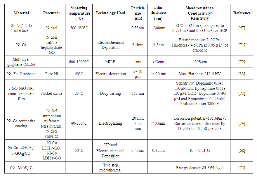 | Table 4. Nickel-graphene ink composites for various printing technologies |
1.3.5. Other Metal Compositions
- Besides commonly used metals like silver, copper, and graphene, nickel shows excellent compatibility with other materials like scandium [76], Manganese [77], YSZ [78], Lithium [44], GCN [34] also. Applications such as SOFC [76], Lithium-ion batteries [44] [79], PSC [46], OLED [44], super-capacitors [34] are implemented using nickel with other metal composites. The inks are printed using IJP [77], 3D printing [80], screen printing [76] [81]. Somalu et al. [82] discovered the effects of binder and solids content on the rheological properties of NiO/10Sc1CeSZ screen-printing inks, and charact-erization of the resultant SOFC anode films, have been studied. These revealed that the particle network strength and moduli of the inks increased with increasing binder and solids content, due to improved particle association. Based on this study, a complex modulus (representing the overall elasticity and tackiness of the inks) of inks, is observed from 500-4000 Pa, which makes it suitable for reliable and high-quality anode films by screen-printing. Also, the ink recovery, ranging from 40-65%, is expected to be sufficient to produce quality films with a minimum number of print defects. From the perspective of ink rheology, screen printability, and performance, inks having 26vol.% solid with 3wt.% binder or 28-30vol.% solid with 2wt.% binder was determined as the most suitable for the manufacture of reliable and high-quality SOFC anode films with a thickness of around 10µm. Chen et al. [77] fabricated micro-spheres using TSS process with Mn-Co-Ni-O ceramic inks. Mn1.2Co1.5Ni0.3O ceramic inks were synthesized using the RM method with high-stability, dispersivity, and homogeneity. The resistance calculated was 634.5-48467KΩ. Williams et al. [83] fabricated SOFC based on cermet anode (Ni-YSZ) and ion-conducting ceramic electrolyte, Yttria-stabilized zirconia (8YSZ) at 800–1000°C. If the temperature is lowered then performance is also degraded. By mixing conducting oxide and metal promoters like gadolinium doped ceria, Ni, Pt, Pd, and Cu has been used to lower the operational temperatures and improve the long-term stability of SOFCs. Two inks were formulated, one water and one propionic acid (PPA) based, used IJP for deposition on the substrate. Both inks were characterized for different parameters like contact angle, power density, etc. PPA-based inks were found to be more suitable for symmetric anode cells. During the sintering process at 800°C, reduction of NiO to Ni, films of 450–600nm thickness were obtained. At 1000°C material shrinkage of 43% was observed. At 1295°C diffusion of the printed YSZ in the substrate was observed. It was found that for nanostructured material, the sintering temperature should be < 800°C. Taylor et al. [80] formulated Fe2O3 and NiO particle-based inks, with an additional H2 reduction step before sintering for 3D printing. No cracks were observed in the sintered structures with 92–98% relative density and 70-80% volume shrinkage. The cellular architecture was fabricated using particle-based inks, with relative densities of 32–49%, low stiffness of 1–6GPa, the strength of 4–31MPa, and high ductility, leading to excellent elastic and plastic energy absorption, when subjected to uniaxial compression. Vera et al. [81] developed a conductive ink including a nickel component, a polycarboxylic acid component, and a polyol component. The conductive ink may include nickel flakes, graphene flakes, glutaric acid, and ethylene glycol. The conductive ink may be printed on a substrate and cured to form a conductive film. A conductive film may include a nickel component and a polyester component. Three nickel inks are formulated: Ink1 (additives styrene and benzoyl peroxide can have reduced sheet resistance) has reduced adhesion, ink2 (the additives styrene, benzoyl peroxide, dimer diamine, cyclohexanol as a solvent can demonstrate polar liquid phobicity, improved adhesion performance) has reduced roughness, ink3 (does not include the additives styrene and benzoyl peroxide, but includes diamine and cyclohexanol as a solvent) demonstrate polar liquid phobicity, improved adhesion performance, and increased roughness. The sheet resistance of ink3 is 0.4-0.5Ω/sq./mil. Wang et al. [44] prepared Li:NiOx by the low-temperature combustion method for the performance of the OLEDs as the HIL. The electrical conductivity and work function is increased by doping Li-ion. When the doping concentration of Li is 5% molar ratio, the Li:NiOx based device obtained higher current efficiency of 55.8cd·A-1 (by 7%) and power efficiency of 57.2mW-1 (by 12%). Yang et al. [46] replaced the volatile organic component of PSC by a cesium inorganic component (CsPbX3) for better thermal stability. However, for α-CsPbI3 and α-CsPbI2Br there is still scope for improvement. Samarium acetylacetonate [Sm(acac)3] was added to CsPbI2Br to fabricate CsPbI2Br Perovskite thin films and to passivate and modulate lattice but also modulate the NiOx/CsPbI2Br interface. PCE of 12.86% was achieved and 90% thermal stability was retained at 85°C for 200h by including Sm(acac)3 to CsPbI2Br PSCs. Paliwal et al. [34] improved the performance of all-solid-state asymmetric supercapacitors (ASSASC) by using GCN (g-C3N4) sheets as electrodes. The GCN nanosheets were synthesized using ammonium carbonate by a polyol process. NiO/GCN was used as the positive electrode and Ni-r-GO as the negative electrode of the capacitor. The NiO/GCN||N-r-GO ASSASC device also offers ~6-times more energy density and ~3-times more rate energy density at a power density of ~6966Wkg–1, over pristine-NiO||N-r-GO ASSASC device. It was found that by slight modification in the configuration of the supercapacitor, surface functionality, electronic conductivity, electro-mechanical stability and matrix accessibility of the hetero-nanocomposite can be enhanced. Gu et al. [79] used Ni for lithium batteries due to its high electrochemical stability. The sheet resistance obtained was 0.25Ω/square and 0.26Ω/square before and after bending of the electrode. The Ni electrodes fabricated for the battery also passed tape testing without material peeling off. After removal of the tape, the sheet resistance measured was 0.25Ω/square. Craton et al. [84] demonstrated the process and characterization of additively manufactured polymer-matrix magnetic nanocomposites of nickel-zinc ferrite (Ni0.5Zn0.5Fe2O4) nanoparticles in a PI matrix aerosol jet printing technique. EDX is used to measure the content of ferrite (18 wt. %) in the composite, fitted simulation models, and ring resonator measurements were used to estimate the permeability. An increase in inductance density of 40% in a 4.5 turn microstrip spiral inductor was obtained. The fully printed inductors demonstrate an inductance density of 4.2 nH/mm2. Rahumi et al. [85] inkjet printed an enhanced SOFC by using NiO-SDC (Sm3+ doped ceria) colloidal ink. Electrical impedance spectroscopy (EIS) demonstrated a reduction, by greater than 80%, in the area-specific resistance of the IJP half-cell in comparison with the Screen-printed half-cell. When nickel is used with other materials, then many new parameters like ink stability, stiffness, power conversion efficiency, and inductance density are evaluated. Table 5 summarizes the use of nickel with other composites using only different printing technologies from aerosol to 3D.
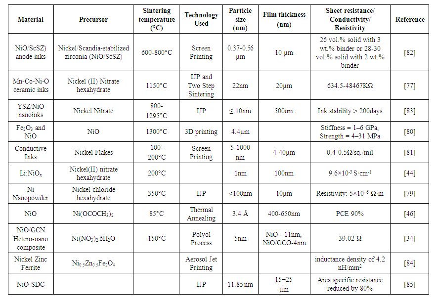 | Table 5. Nickel and other composites for conductive inks |
1.4. MOD Ink
- MOD (Metal-organic decomposition) inks are also known as particle-free ink or precursor ink. These inks are prepared by using metal salts as precursors, complexing agents, and solvents. As per the author’s knowledge, very little literature is available for nickel MOD ink. The particle size of nanoparticles formed after the sintering process is in the nm range.
1.4.1. Nickel MOD Ink
- Dylan [87] formulated particle-free nickel ink capable of metalizing highly pure Ni at temperature <100°C for plastic and paper substrates. Three sets of inks were developed with different solvents. Ink 1 used ammonia with water and glycerol gives 10wt% metallization; ink2 used NaOH and glycol produced sedimentation at the bottom; ink3 used TMAH and glycol which gives 70wt% metallization. Table 6 represents the use of nickel MOD ink for the RIJP process.
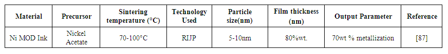 | Table 6. Nickel MOD ink for RIJP process |
1.4.2. Nickel-Silver MOD ink
- Mahajan et al. [88] developed well-aligned nickel nanowires with unique and customizable structures on different substrates for electronic and magnetic applications. The template-free approach is used for flexible, enhanced anisotropic electrical and magnetic properties. The reduction of Ni was observed in the presence and absence of a magnetic field. Interestingly, a reduction in the presence of a magnetic field produced pure, template-free, aligned Ni nanowires. In this way, large areas of aligned Ni nanowires were produced, using only weak magnetic fields. Table 7 represents the use of nickel-silver MOD ink using the IJP process.
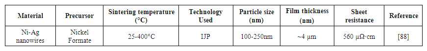 | Table 7. Nickel-silver MOD ink using IJP process |
1.4.3. Nickel-Copper MOD Ink
- Mahajan et al. [26] Nickel MOD ink and copper MOD ink is formulated using metal formate salts. Nano alloys are synthesized using both inks with the composition of Cu8Ni92. The relative resistance of copper is increased with the number of passes in sintering. The resistance is decreased for the nanoalloy ink. Table 8 represents nickel-copper MOD ink used for the IJP process.
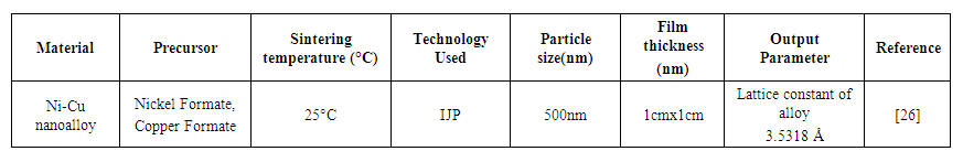 | Table 8. Nickel-Copper MOD ink used for IJP process |
2. Conclusions
- After doing the extensive literature survey it can be concluded that the nickel conductive ink has received remarkable progress. When both types of nickel conductive inks nanoink (particle-based) and MOD ink (particle-free) were reviewed, there is still plenty of room for the development of nickel conductive inks. The lowest particle size used is 5nm for particle-based ink and 1nm for particle-free ink. Nickel ink can be formulated and combined with other materials, such as silver, copper, and graphene. Out of all materials, graphene is preferred because of its excellent conductive properties due to sp2 hybridization. Nickel-graphene composites exhibit strong hybridization between the 2p orbital of graphene and the 3d orbital of nickel. Lattice mismatch of ~1.2% was observed in the crystal structure. The metal separation between the two materials is 0.21nm. The strong chemical interaction between graphene and nickel improves electrical conductivity. The ink formulated can be used for various printed electronic applications. Temperature detectors, capacitors have already emerged, and more are anticipated. Inkjet printing has numerous advantages of high material utilization, simple setup, and high-speed printing at low cost over screen printing, spin coating, etc. techniques. According to the author’s knowledge very less work is done on nickel MOD ink which opens a new area of research for forthcoming researchers. Future innovations in material selection, printing, and post-processing methods will grow to widen the area of application and match the growing demands of the printing industry.
ACKNOWLEDGEMENTS
- I would like to express my deep and sincere gratitude to my research supervisor, Dr. Hari Murthy, Assistant Professor, CHRIST (Deemed to be University), Bengaluru, for giving me the opportunity to do research and providing invaluable guidance throughout this research.