Nicholas O. Ongwen1, Andrew O. Oduor1, Elijah O. Ayieta2
1Department of Physics and Materials Science, Maseno University, Maseno, Kenya
2Department of Physics, University of Nairobi, Nairobi, Kenya
Correspondence to: Nicholas O. Ongwen, Department of Physics and Materials Science, Maseno University, Maseno, Kenya.
| Email: |  |
Copyright © 2019 The Author(s). Published by Scientific & Academic Publishing.
This work is licensed under the Creative Commons Attribution International License (CC BY).
http://creativecommons.org/licenses/by/4.0/

Abstract
Spray Pyrolysis Technique was used in depositing thin films of cadmium stannate, doped with iron metal. The precursor solutions used were sprayed onto the pre – heated glass slides that were kept at a constant temperature of 450°C. The transmittance and reflectance measurements were made in the spectral wavelength range of 300 – 1100 nm. It was found out that both the concentration of the reactants and doping had an effect on the optical properties of the deposited thin films. At the upper end of the visible spectrum (718 nm wavelength), the values of the optical constants were: Transmittance of up to 70.45%, thickness of 323 – 594 nm, refractive index of 2.108 – 3.542, absorption coefficient of 7.385 x 103 cm-1 – 2.2784 cm-1, extinction coefficient of 0.042 cm – 0.130 cm and a band gap energy of 3.9 eV.
Keywords:
Cadmium stannate, Iron – doped, Optical properties of cadmium stannate, Optical conductivity, Concentration of reactants on optical properties
Cite this paper: Nicholas O. Ongwen, Andrew O. Oduor, Elijah O. Ayieta, Effect of Concentration of Reactants on the Optical Properties of Iron – Doped Cadmium Stannate Thin Films Deposited by Spray Pyrolysis, American Journal of Materials Science, Vol. 9 No. 1, 2019, pp. 1-7. doi: 10.5923/j.materials.20190901.01.
1. Introduction
With the advancement in technology and the ever growing need for optical coatings for varius applications, there is a lot of research going on lately about possible compounds that can produce transparent semiconductor thin flms (TF’s). Tin doped indium oxide, also known as Indium Tin oxide (ITO), is the most commonly used and also the most widely known antireflective coating material [1]. However, this compound (ITO), just like the other transparent conducting materials, has its drawbacks. Fistly, indium is very expensive to purchase, making the ITO to be expensive and secondly, indium is not readily available. These drawbacks limit the production and use of ITO as a tansparent conducting material [2]. Cadmium stannate (Cd2SnO4) is of particular interest because it improves the transparency of the glass compared to the other conducting materials like cadmium telluride (CdTe), Copper Indium Gallium Diselenide (CIGS) and the ITO, which are used for the fabrication of the glass. Characterization of Cd2SnO4, doped with iron (Fe), which has been studied to produce transparent TF’s of iron II oxide within the spectral wavelength range of 600 – 2000 nm [3], provides an opportunity of obtaining a variety of materials that can be used as antireflective.
2. Experimental Details
2.1. Film Preparation
The microscope glass substrates used in the experiment were cleaned by dipping them in AquaRegia (3:1 of hydrochloric acid: nitric acid) for 12 hours, after which they were removed and then rinsed using deionised (DI) water [4]. Whatman lens cleaning tissue, model number 105 (100 x 150 mm) was used to wipe the glass substrates dry. The precursor solutions used were cadmium acetate dihydrate (99.99% pure), tin II chloride dihydrate (99.99% pure) and iron III chloride (98% pure), all obtaied from Central Drug House (CDH) (P) Ltd. 7/28 Vardaan House, Daryaganj, New Delhi – 110002 (India). All the three compounds were dissolved separately in absolute ethanol (99.99% pure), after being weighed accurately using the METTLER TOLEDO PB 303 weighing balance. The cadmium acetate and tin II chloride solutions were prepared at concentrations of 0.1, 0.2 and 0.3M. The dopant (iron III chloride) was prepared at a concentration of 0.1M. The cadmium acetate and tin II chloride solutions were then mixed at ratios of 1:1, 2:2 and 3:3 by concentration. This formed a white precipitate. 3 ml of dilute hydrochloric acid (2M) was then added to the precipitate, after which it dissolved to form a colourless solution of Cd2SnO4 [5]. The different concentrations of the colourless solution (Cd2SnO4), were finally mixed with the dopant at 0 – 8% by volume of the Cd2SnO4 solution. The final solution was then poured into the gun, then sprayed onto the pre – heated microscope glass substrates by SPT (number HO-TH-04) on a plate that was kept at a constant temperature of 450 ± 5°C (figure 1 below).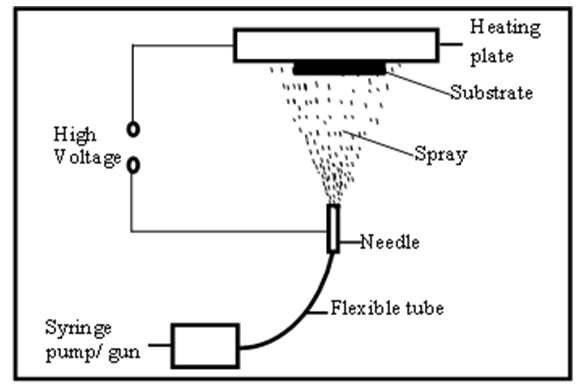 | Figure 1. Schematic diagram of the deposition process |
2.2. Measurements
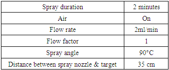
The optical transmittance and reflectance of the deposited TF’s were measrued using the Shimadzu UV-VIS-NIR Spectrophotometer - SolidSpec 3700 DUV in the spectral wavelength range of 300 – 1100 nm. The parameters that were kept constant during the experiment are shown in table 1 below. From the transmittance and reflectance, the optical constants (absrorption coefficient, extinction coefficient, dielectric constant, refractive index and band gap energy) were determined.Table 1. Parameters that were kept constant during the experiment
 |
| |
|
3. Results and Discussion
3.1. Transmittance and Reflectance
The curves in figures 2 & 3 below show the transmittance and reflectance that were obtained.From figure 2 below, it is clear that transmittance is low at short wavelength (high photon energies). Figure 2 below shows that transmittance decreases with increase in the concentration of Cd2SnO4 (film thickness). The concentration of 0.1M Cd2SnO4 has the highest transmittance of 70.45%, while that of 0.3M has the lowest transmittance of 57.09% at the upper end of the visible spectrum (718 nm). This is because the thicker films absorb more of the incident light than the thinner ones, leading to low transmission, with the extent of absorption increasing with increase in the film thickness [6]. The decrease in transmittance with increase in the thickness of the films is also due to the crystallization of the film structure by increasing the grain size [7]. There was negligible transmittance at shorter wavelength below 300 nm. This is because most of the incident light is absorbed in this wavelength range [8]. Reflectance on the other hand, generally decreased with decrease in the concentration of Cd2SnO4. The 0.1M Cd2SnO4 gave a maximum reflectance of 10.34%, while the 0.3M films gave a maximum of 14.20% (figure 2 below).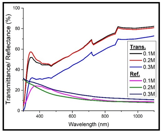 | Figure 2. Transmittance and reflectance against wavelength for the undoped cadmium stannate thin films |
When the films were heavily doped with iron, it was observed that the transmittance still decreased with increase in the concentration of Cd2SnO4, while the reflectance still increased with increase in the concentration (figure 3 below). 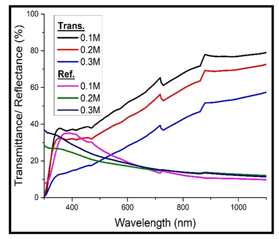 | Figure 3. Transmittance and reflectance against wavelength for the heavily doped cadmium stannate thin films |
However, the values of the transmittance for the undoped TF’s (figure 2 above) are higher than those of the heavily doped thin films (figure 3 above).The 0.1M Cd2SnO4 gave a maximum transmittance of 65.36%, while the 0.3M gave 39.40% upon doping. Reflectance on the other hand, gave a maximum value of 13.31% for the 0.1M and 15.04% for the 0.3M Cd2SnO4 respectively after doping. The decrease in transmittance and increase in the reflectance upon doping is because doping introduces free electrons into the structure of Cd2SnO4, which then absorb more light in the visible spectral wavelength range.
3.2. Film Thickness
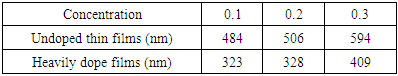
The thickness of the films formed was measured for the different concentrations. Table 2 below gives the results.Table 2. Thickness for different concentrations of cadmium stannate thin films
 |
| |
|
Table 2 above shows that the film thickness increased with increase in the concentration of Cd2SnO4. This was as expected, since the higher the concentration, the higher the number of particles of the solute in the solution that is deposited onto the substrate [9]. On heavily doping, the thicknesses of the films still increasd with increase in the concentration of Cd2SnO4. However, the values of the heavily doped films were found to be less than those of the undoped films. This might have been brought about by the fact that the dopant fit into the voids of Cd2SnO4.
3.3. Absorption Coefficient
The absorption coefficients of the deposited TF’s were determined from the formula:  | (1) |
Where A is the absorbance and d is the film thickness in cm.The absorbance A is given by:  where T is the transmittance.
 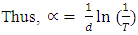 | (2) |
As can be observed in figure 4 below, the absorption coefficient increased with increase in the photon energy, increasing sharply at high energies above 3.8 eV. This implies that the absorption coefficient increased with a decrease in the transmittance, since the films become more absorbing at short wavelength range [8]. The absorption coefficient was also observed to rise sharply at energies above 3.8 eV. The sharp rise in the absorption coefficient at photon energy above 3.8 is caused by the fact that this energy range approaches the band gap energy of Cd2SnO4 (3.9 eV in this work), the energy above which the tightly bound electrons in the material become mobile and jump from the valence band to the conduction band. The free electrons then absorb most of the incident photon energy [10].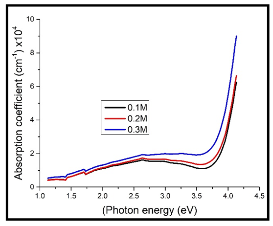 | Figure 4. Absorption coefficient against photon energy for the undoped thin films |
When the TF’s were heavily doped, the results in figure 5 below were obtained.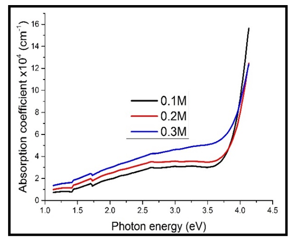 | Figure 5. Absorption coefficient against photon energy for the heavily doped thin films |
Upon doping, the absorption coefficient was found to increase with increase in the concentration of Cd2SnO4 (figure 5 above), just the same as those that were not doped (figure 4). However, the values of the absorption coefficient for the heavily doped TF’s are higher than those of the undoped TF’s. This can be attributed to the effect caused by the dopant (the free electrons introduced into the films by the dopant, that absorb more of the photon energy), which reduces the transmittance, thus leading to an increase the absorption coefficient.
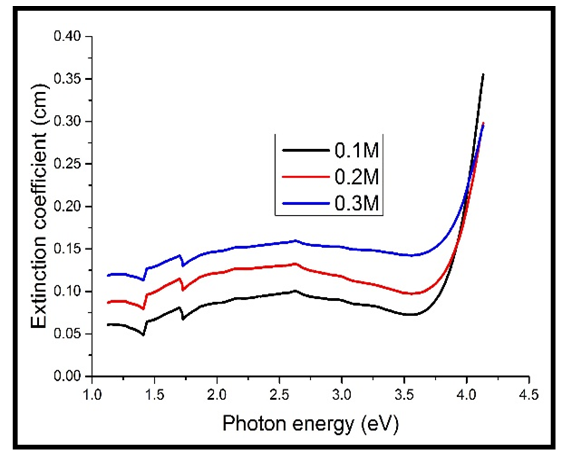
3.4. Extinction Coefficient
Extinction coefficient is the imaginary part of the complex refractive index [11]. The extinction coefficient (k) of the films was obtanied from the absorption coefficient (α) and wavelength (λ) using the equation: | (3) |
The extinction coefficient was found to increase with increase in the photon energy, rising sharply at energies above 3.7 eV. The extinction coefficient also increased with increase in the concentration of Cd2SnO4, just like for the absorption coefficient in figures 4 & 5 above. This is because the extinction coefficient is directly proportional to absorption coefficient according to equation 3 above.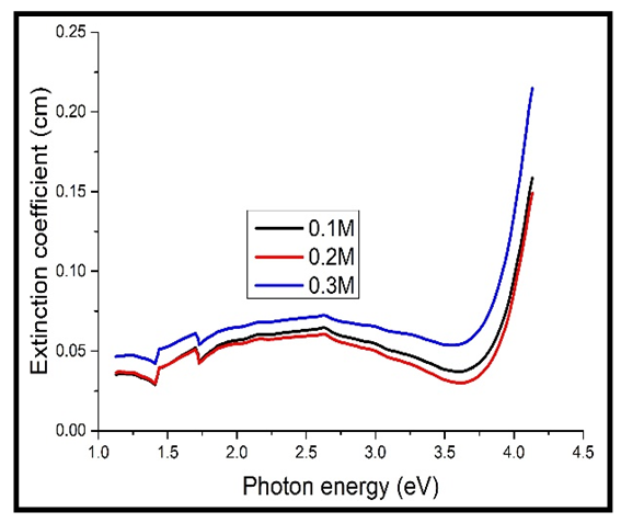 | Figure 6. Extinction coefficient against photon energy for the undoped thin films |
 | Figure 7. Extinction coefficient against photon energy for the heavily doped thin films |
The values of the extinction coefficient for the heavily doped TF’s still increased with increase in the concentration of Cd2SnO4, same to those of the undoped TF’s. However, the values for the heavily doped TF’s were higher than those of the undoped TF’s (comparing figures 6 & 7 above). This is because the dopant contains free electrons, which absorb more of the incident light in the visible spectrum.
3.5. Refractive Index
Refractive index (n) for the TF’s was calculated using the Swanepoel’s envelope method [12]. The maximum transmittance (Tmax) and the corresponding minimum transmittance (Tmin) were obtained from the envelope. From the two values, n was obtained by: | (4) |
 | (5) |
 | (6) |
Here, Ts is the transmittance of the bare glass substrate, without the TF. Below are the graphs of refractive index against wavelength for the different thin films in the wavelength range of 300 – 1100 nm.The refractive index of the TF’s was observed to decrease exponentially with increase in wavelength. This is due to less absorption by the films at the long wavelength range. At longer wavelength range, the refractive index tends to be constant. This agrees well with some of the previous work [8, 13]. The decrease in the refractive index with increase in the wavelength can stll be attributed to the effects of surface and volume imperfections in the films [14]. At long wavelength range (low energies), the refractive index tends to be constant. This is because long wavelength region is the region of low absorption [8].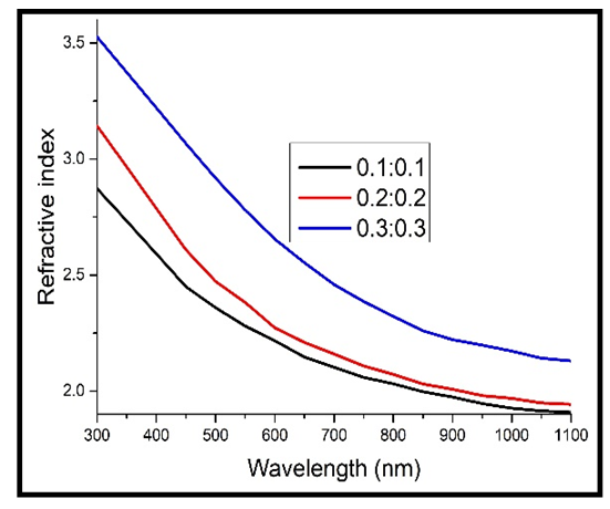 | Figure 8. Refractive index against wavelength for the undoped thin films |
Refractive index was also observed to increase with increase in the concentration of Cd2SnO4 (film thickness). As can be observed in figure 8 above, the concentration of 0.1M produced TF’s with the lowest values of the refractive index, while that of 0.3M produced the highest. This behaviour can be explained on the basis that increase in film thickness makes the film denser (increases the packing density), which in turn decreases the propagation velocity of light through them, since refractive index represents the ratio of light velocity through a vacuum to velocity through a material medium [15]. This behaviour accompanies the increase in the film thickness (decreased band gap energy value) according to inverse relation between refractive index and band gap energy.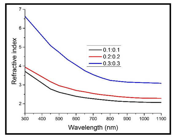 | Figure 9. Refractive index against wavelength for the heavily doped thin films |
Doping generally improved the refractive indices of the deposited films, with the concentration of 0.3M still recording the highest values, while 0.1M still recording the lowest values (figure 9 above). This is in line with some of the previous work done [9] and can be attributed to the increase in the reflectance. The refractive index was also observed to rise sharply at short wavelengths (below 600 nm), which can be attributed to the higher reflectance at shorter wavelengths than at longer wavelengths.
3.6. Real Part of the Dielectric Constant
The real part of the dielectric constant was determined using the formula: | (7) |
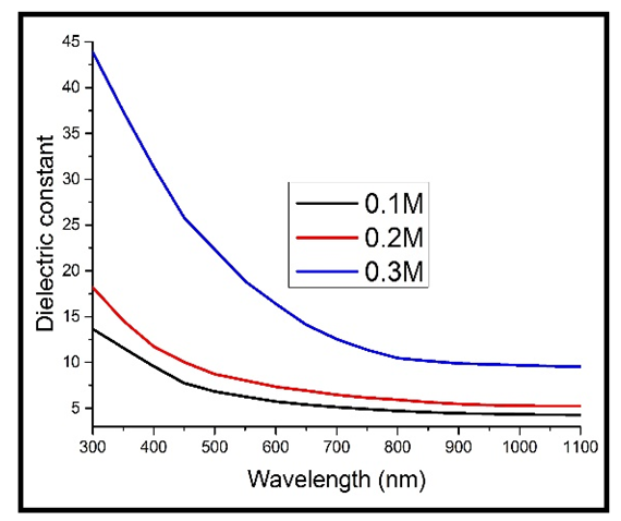
Where n is the refractive index and k is the extinction coefficient. The dielectric constant was observed to reduce exponentially with increase in the wavelength, same as the refractive index in figures 8 & 9 and extinction coefficient in figures 6 & 7. This is because the dielectric constant is directly related to the extinction coefficient and refractive index according to equation 7 above. At longer wavelengths, the dielectric constant tends to be constant. The decrease in the dielectric constant with increase in wavelength implies that the TF’s become more conducting to electricity, which also implies that the band gap energy of the TF’s reduces with increase in the wavelength [16].The dielectric constant also increased with increase in the concentration of Cd2SnO4. This is due to the free carrier absorbance of the TF’s, which leads to a shift in the Fermi level [8].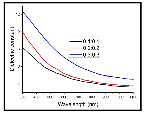 | Figure 10. Real part of the dielectric constant against wavelength for the undoped thin films |
 | Figure 11. Real part of the dielectric constant against wavelength for the heavily doped thin films |
Upon doping, the dielectric constant still increased with increase in the concentration of Cd2SnO4. However, the values of the dielectric constant for the heavily doped TF’s (figure 11) are higher than those of the undoped TF’s (figure 10). This implies that there was an increase in the absorption (less transmittance) in the material, caused by an increase in the free charge carrier concentration, which was brought about by the free electrons introduced into the TF’s by the dopant. The increase in the dielectric constant upon doping is in line with the various published work, including those of Bushra and Shalkal [15].
3.7. Band Gap Energy
The Tauc relation was used to determine the optical band gap energy of the deposited TF’s. Acording to Ellingson and Heben [17], a direct band gap energy is given by: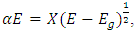 from which we get:
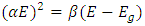 | (8) |
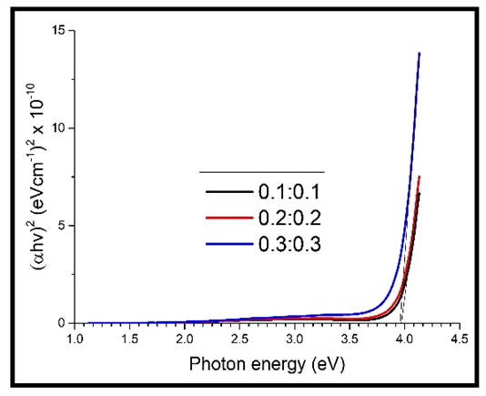
Graphs of  were plotted against photon energy (E = hυ) in eV to obtain figures 12 & 13 below.
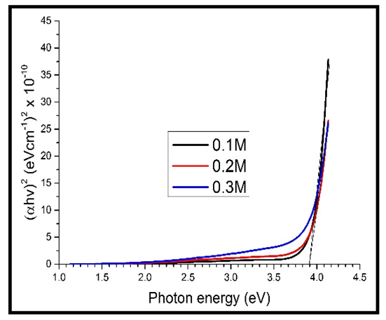 | Figure 12. A graph of  against photon energy (E = hυ) in eV for the undoped thin films against photon energy (E = hυ) in eV for the undoped thin films |
 | Figure 13. A graph of  against photon energy (E = hυ) in eV for the heavily doped thin films against photon energy (E = hυ) in eV for the heavily doped thin films |
The graph in figure 12 above is non – linear, implying that the transition is allowed and direct. All the different concentrations of Cd2SnO4 gave a band gap energy of 3.9 eV. This shows that the films had very little or no structural gaps [7]. The value of the band gap energy obtained in this research in agreement with some of the previous work [9]. The deposited thin films gave a direct allowed transition, that is, the value of r from the equation:  is ½ [17]. All the TF’s gave a band gap energy of 3.9 eV upon doping. This implies that the films had structural gaps filled, with little or no defects [15]. The band gap energy obtained in this work are high (greater than 3.2 eV), which is good for making front panel of thin film solar panels, since the high band gap energy helps in avoiding absorption of light over most of the solar spectrum [18].
4. Conclusions
The transmittance of the deposited TF’s increased with increase in the wavelength. The absorption coefficient was observed to increase with increase in the photon energy, increasing sharply at high energies above 3.8 eV. The film thickness increased with increase in the concentration of Cd2SnO4. When heavily doped, the thickness of the TF’s was also observed to increase with increase in the concentration of Cd2SnO4. However, the thickness of the heavily doped TF’s was lower than that of the undoped TF’s. The absorption coefficient generally increased with increase in the concentration of the precursor solutions (film thickness), both for the undoped and the heavily doped TF’s. The extinction coefficient was found to increase sharply at low wavelengths below 320 nm (high energies above 3.8 eV). The extinction coefficient was also observed to increase with increase in the concentration of Cd2SnO4. On doping, the extinction coefficient was observed to increase also. The refractive index generally decreased with increase in the wavelength. At longer wavelengths, the refractive index tended to be constant. The refractive index was also observed to increase with increase in concentration of Cd2SnO4. The real part of the dielectric constant was found to reduce with increase in wavelength. At longer wavelength, the dielectric constant tended to be constant. The dielectric constant also increased with increase in the concentration of Cd2SnO4. Upon doping, the dielectric constant also increased. A band gap energy of 3.9 eV was obtained for both the undoped and the heavily doped TF’s.
ACKNOWLEDGEMENTS
The authors of this research would like to thank the National Research Fund (NRF) for providing funds to carry out the research and to publish it (2017).More thanks to Mr. Boniface Muthoka, a laboratory technician at the University of Nairobi, for providing technical assistance and experimental support when carrying out the experiment.
References
| [1] | M. Mazzeo, F. Mariano, G. Gigli, High efficiency ITO-free flexible white organic light-emitting diodes based on multi-cavity technology. Org. Electron. 4, 2840 – 2846 (2013). |
| [2] | C. Bright, Transparent conductive thin films. Opt. Thin Films Coat. 1, 741 – 788, (2013). |
| [3] | M. Ohring, The material science of thin films. (Academic Press, London, 1992). |
| [4] | M. Al-Kuhaili, M. Saleem, SMA. Durrani, Optical properties of iron oxide thin films deposited by reactive evaporation of iron, J. Alloys Comp, 521, 178 – 182 (2012). |
| [5] | G. Shugar, J. Ballinger, Chemical Technicians’ Ready Reference Handbook. (McGraw- Hill, New York, 1996). |
| [6] | K. Krishna, K. Kamamurthi, E. Elangovan, Novel procedure to prepare cadmium stannate films using spray pyrolysis technique for solar cell applications. (University of Lisbon, Caparica, (2010). |
| [7] | N. Eman, S. Igbal, M. Alias, Characterization of cadmium tin oxide thin films as a window layer for solar cell. Int. J. Appl. Innov. Eng. Man., 2, 189 – 194 (2013). |
| [8] | A. Mulama, J. Mwabora, Optical properties and raman studies of amorphous Se-Bi thin films. African Rev. of Phys., 9, 32-38, (2014). |
| [9] | A. Cristaldi, A. Gulino, E. Maria, Structural, electronic and electrical properties of yttrium - doped cadmium stannate. J. Phys. Chem., 116, 3363 - 3368 (2012). |
| [10] | T. Mohammad, Optical properties of cadmium stannate thin film prepared by pyrolytic process. Solid State, 72, 1043 – 1046 (1989). |
| [11] | I. Newton, Opticks: or, A treatise of the reflections, refractions, inflections and colours of light (William Innys, London, 1730). |
| [12] | E. Shaaban, I. Yahia, E. El-Metwally, Validity of swanepoel's method for calculationg the optical constants of thin films, Acta Phys. Pol. A., 121, 628 – 635 (2012). |
| [13] | D. Dorranian, D. Laya, G. Mosayebian, Optical characterization of Cu3N thin films with swanepoel method. J. Theor. and Appl. Phys., 6, 1 – 9 (2012). |
| [14] | P. Bhuvaneswari, M. Velusamy, Effect of fluorine doping on the structural, optical and electrical properties of spray deposited cadmium stannate thin films. Mater. Sci. Semicond. Proc., 16, 1964 – 1970 (2013). |
| [15] | A. Bushra, I. Shalkal, Structural and optical properties of SnS thin films. J. Nano. Adv. Mater. 2, 43-49 (2013). |
| [16] | A. Esmat, I. Saad, Dielectric properties of molybdenum oxide thin films. J. Opto. Adv. Mater. 7, 2743 – 2752 (2005). |
| [17] | R. Ellingson, M. Heben, Absorption coefficients of semiconductor thin films. Retrieved from Wikipedia: http://en.wikipedia.org/wiki/Sheet_resistance. (November, 2011). |
| [18] | W. Siefert, Thin solid films. J. Electron., 120, 265-271 (1984). |

 Abstract
 Reference
 Full-Text PDF
 Full-text HTML