Geoffrey Gitonga Riungu1, Mathew Munji1, Robinson Musembi2, Nelson Mugambi1, John Gitonga1
1Department of Physics, Kenyatta University, Nairobi, Kenya
2Department of Physics, University of Nairobi, Nairobi, Kenya
Correspondence to: Geoffrey Gitonga Riungu, Department of Physics, Kenyatta University, Nairobi, Kenya.
| Email: |  |
Copyright © 2017 Scientific & Academic Publishing. All Rights Reserved.
This work is licensed under the Creative Commons Attribution International License (CC BY).
http://creativecommons.org/licenses/by/4.0/

Abstract
SnxSey and SnO2: Co thin films were deposited on clean glass slides by spray pyrolysis technique at 400 K and 500 K respectively. SnxSey films were deposited using 0.05M SnCl4:2H2O and 0.05M 1-1 dimethyl selenourea (C3H8N2Se) in a mixture of deionized water and isopropyl alcohol in the ratio of 1:3. SnO2 films were prepared by dissolving 0.025 M of Tin IV chloride 2 hydrate (SnCl4:2H2O) in a mixture of deionized water and ethanol in the ratio of 1:1. Doping was done using Co (NO3)2:6H2O from (0-10%) wt. Transmittance and reflectance data in the range 280nm-1200nm was obtained using a 3700 UV-VIS-NIR shimadzu spectrophotometer. The calculated band gap (Eg) of SnSe ranged from 1.98eV to 1.38eV with highest absorbance in visible region of up to 47.51% and relatively lower transmittance and reflectance. Transmittance for SnO2: Co thin films was >80% for all films with highest transmittance in visible region at 4% doping. Band gap of SnO2: Co thin films decreased from 3.56 eV at 0% doping to 3.22 eV at 6% doping. SnSe /SnO2: Co (4% doping) p-n junction solar cell was fabricated with open circuit voltage of 0.62V, short circuit current (Isc) of 1.16mA, and conversion efficiency (η) of 0.525%.
Keywords:
Spray pyrolysis, Selenourea, Co-doping, Tin oxide, Thin films
Cite this paper: Geoffrey Gitonga Riungu, Mathew Munji, Robinson Musembi, Nelson Mugambi, John Gitonga, Optical Characterization of SnxSey /SnO2: Co P-N Junction Deposited by Spray Pyrolysis for Photovoltaic Application, American Journal of Materials Science, Vol. 7 No. 6, 2017, pp. 258-265. doi: 10.5923/j.materials.20170706.05.
1. Introduction
The world’s energy demand is increasing everyday due to rapid population growth. This has led to increased demand for energy, decline in fossil fuel stocks, more production of carbon IV oxide emissions and global warming. It is the search for carbon free power that provides a strong need for pursuing solar energy conversion [1]. Photovoltaic hold great hopes towards solving energy crisis since they are environment friendly, sunlight is free, abundant and not likely to be exhausted in the near future. Solar cells fabricated using tin metal such as Tin-Zinc, Tin-Antimony, Tin-Cadmium and Copper-Tin alloys are stable and their operation lifetime is long [2].Tin Selenide is a IV-VI semiconductor with a narrow band gap  It is suitable for a wide range of optoelectronic applications e.g. photovoltaic, memory switching devices, light emitting diodes, holographic recording system etc. The compounds for SnSe are readily available. The structure of SnSe thin film strongly influences the optical and electrical properties dependent on preparation method. SnSe thin films indicate semiconductors behavior with p-type conductivity. It has also a superior optical transmission in the range of 0.5-20 μm capable of improving conductivity and increasing current flow in a p-n junction [3]. Thin films of Tin Selenide and Tin diselenide have been deposited using the ultrasonic spray pyrolysis technique, the films have a direct band gap, low resistivity and p-type conductivity [4].The optical studies showed that SnxSey has a direct band gap energy of Eg=1.26 eV and an improbable indirect band gap. Further photosensitivity increases with level of illumination. The photo decay in these vacuum deposited films reveals the presence of deeper localized states and carrier lifetime of SnxSey to be 1.6 seconds [5]. This is a critical parameter for the performance of a solar cell. In their attempt to prepare semiconducting tin selenide thin films by heating, [3] found out that the optical band gaps for SnSe2 and SnSe were 1.27 eV and 1.03 eV respectively. They also noted that SnSe2 and SnSe2/SnSe composite materials can be efficient absorber layers in solar cells for an optical band gap of 1 – 2.7 eV and electrical conductivity of 0.01-0.25 Ω-1 cm-1.Tin based solar cells and their alloys were studied and found to exhibit good properties and high efficiency solar cell materials. They have direct band gap and high absorption coefficient compared to silicon and gallium arsenide [6].Upon cobalt doping on SnO2, the Hall mobility improves gradually. Decrease in electrical transport is also reported. This unexpected effect induces a dramatic drop in the electrical resistivity [7]. Effects of Co-doped SnO2 thin films were investigated and observed that Co addition controlled the crystallinity of the SnO2 [8]. The direct optical band gap (Eg) of powders for Co-doping level in the range 0 to 12 mol% were decreased from 3.19 to 2.97 eV respectively [9]. In this study, we report on the deposition and the characterization of tin selenide and co–doped SnO2 thin films prepared by spray pyrolysis for photovoltaic applications. The work gives an insight on the optical properties of prepared thin films with varying selenium ratios and cobalt dopant respectively. Transmittance and reflectance have been evaluated in the UV–Vis–NIR spectral range. In addition, a solar cell (SnSe/SnO2: Co) was fabricated.
2. Experimental Procedure
2.1. Cleaning of Substrate
Microscope glass slides were used as the substrate. The glass slides were cleaned by first soaking them in soapy water solution. They were sonicated for 30 minutes in a sonicator machine and then rinsed using distilled water. After drying the substrates were stored in desiccator ready for thin film deposition.
2.2. Precursor for SnO2: Co Thin Films
0.025M of tin IV chloride 2 hydrate SnCl42H2O (98% from Sigma Adrich supplies, India) was prepared by dissolving 1.485g in 250 ml mixture of absolute ethanol (99.99% from Sigma Adrich supplies, India and distilled water in the ratio 1:1. A few drops of hydrochloric acid were added to the starting solution in order to achieve complete dissolution of SnCl2·2H2O [9, 10]. The solution was left to age for one week. Doping source was 0.025M cobalt nitrate 6 hydrate (Co (NO3)2:6H2O) prepared by dissolving 1.8189g in a 250ml mixture of distilled water and ethanol in the ratio of 1:1. Doping from (0-10%) wt was done. To calculate (0-10%) wt. doping, molar weight of the element in relation to molar weight of the compound was computed as follows;  | (1) |
where  is the mass in grams of element 1 and
  is the molar mass of the compound.Similarly concentration of atoms of element 1 present in a compound containing two elements 1 and 2 denoted by C1 is given by;
 | (2) |
where  is molar mass of element 1 and
  is molar mass of element 2.
2.3. Precursor for SnxSey Thin Films
0.05 M SnCl2:2H2O was prepared by dissolving 2.82 g in 250 ml of distilled water and isopropyl alcohol in the ratio 1:3. 0.05M solution of 1–1 dimethyl-selenourea (C3H8N2Se) (99% from sigma Adrich, India) was also prepared by dissolving 0.378 g in 100 ml of deionized water and isopropyl alcohol in a ratio of 1:3, such that the atomic ratio between Sn:Se was 1:1. A few drops of hydrochloric acid were added to the starting solution in order to achieve complete dissolution of SnCl2:2H2O. The two solutions were mixed to achieve different ratios of Sn:Se by mass , 0.4 to 1.4.
2.4. Deposition of Thin Films
Spray pyrolysis technique was used to deposit thin films. The set up used was a laboratory assembled spray pyrolysis system shown on figure 1. Spraying was done in a fume chamber, a rotating electric hot plate, spray nozzle of diameter  mm, input gas valve, gas compressor, gas flow meter, thermocouple and a pressure gauge.
 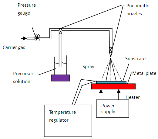 | Figure 1. Schematic diagram of spray pyrolysis technique |
Cobalt doped SnO2 thin films were prepared by spraying 30 ml of the precursor solution on clean slides. Precursor solution was sprayed onto a pre heated substrate at a temperature of 500 K. The deposition parameters as adopted from [9, 11] were;Ÿ Carrier gas; compressed air at 2.5 bars.Ÿ Amount sprayed; 30ml.Ÿ Spray rate; 6ml/min.Ÿ Nozzle to substrate distance; 25cmSnSe thin films were prepared by spraying 40 ml of precursor solution onto a pre heated substrate at a deposition temperature of 400 K. Other deposition parameters as in [11] are;Ÿ Carrier gas; compressed argon at 4.41 bars.Ÿ Amount sprayed; 40ml.Ÿ Spray rate; 8ml/min.Ÿ Nozzle to substrate distance; 20cmAfter spraying, the films were allowed to cool on the hot plate gradually before removal.
2.5. Fabrication of SnSe/SnO2: Co Solar Cell
The solar cell with glass/SnO2: Co /SnSe/Al was fabricated in stages. The window layer of thin transparent conducting SnO2: Co film was deposited onto a clean glass substrate. A thin film of SnSe deposited on the same substrate to form an absorber layer. Aluminum was coated on SnSe film to form the back contact. Figure 2 shows the fabricated cell. A solar cell simulator fitted with dichroic reflectors was used to obtain data. The current-voltage characteristics was plotted. 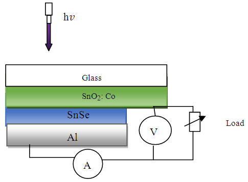 | Figure 2. Schematic diagram of SnO2: Co/SnSe/Al P-N solar cell |
3. Results and Discussion
3.1. Optical Analysis of SnxSey Thin Films
The experimental data for transmittance and reflectance were obtained directly from UV VIS NIR Spectrophotometer. Data obtained was recorded in the UV probe software and excel spread sheets. Origin version 8.0 was used to plot the spectra from raw data. Figure 3 shows transmittance spectra for tin selenide thin films.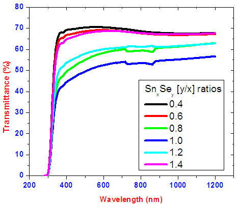 | Figure 3. Graph of transmittance versus wavelength for different ratios of SnxSey thin films |
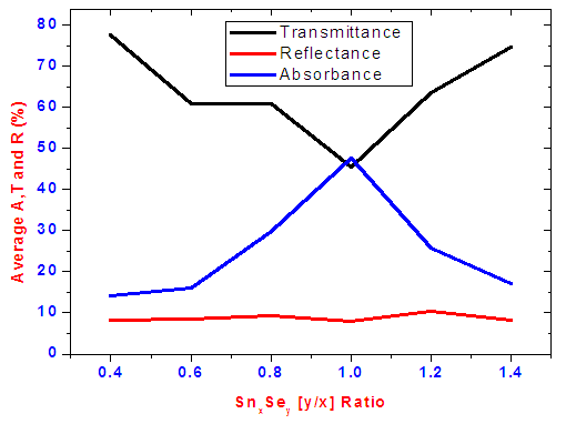
Transmittance against wavelength for SnxSey lies between 50-70% in the visible region. It is observed that SnxSey [y/x] ratio 1.0 had the lowest transmittance. Within the visible range to near infrared a weird peak at slightly above 800nm occur due to change of detectors since the SolidSpec-3700DUV spectrophotometer is equipped with a photomultiplier tube detector for the ultraviolet and visible regions, and InGaAs and PbS detectors for near infrared region. The photomultiplier tube detector is switched to the InGaAs where the default switching wavelength is 870nm [10]. The decrease in transmittance as selenium increases is as a result of decrease in band gap energy. This results to absorption of most of the photons with energy more than forbidden energy. The thin films reflectance is low as shown in figure 4 and lies mainly below 10% in the visible region. Low reflectivity can be attributed to higher band edge absorption of light energy by the films thus generating electron-hole pairs as well as transmittance for photons with energy lower than band gap energy. The averages of transmittance (T), reflectance (R) and Absorbance (A) in visible region is shown in figure 5. A sample of SnxSey [y/x] ratio 1.0 had the highest average absorbance of 47.51%.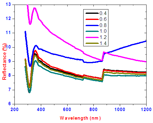 | Figure 4. Graph of reflectance versus wavelength for different ratios of SnxSey thin films |
 | Figure 5. Average transmittance, Absorbance and reflectance in visible region |
Scout software [13] was used to estimate the refractive indices, extinction coefficients and the band energies. The band gap energy values were obtained using Tauc’s relation as shown;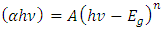 | (3) |
Since SnSe is a direct allowed band gap then n assumes a value of ½. The extrapolated linear graph cuts Energy axis at a point which gives the Band gap of the sample. Figure 6 shows band gap of SnSe from Tauc’s relation. The optical band gap energy for all the samples ranged between 1.38-1.97 ± 0.05 eV with the Sn:Se ratio of 1.0 having the lowest band gap energy.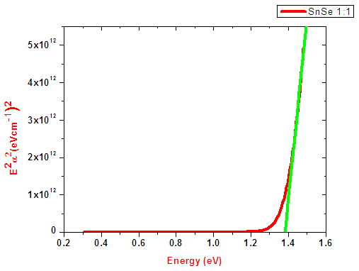 | Figure 6. Band gap energy of SnxSey [y/x)] ratio 1.0 from Tauc’s relation |
Generally the thin films exhibit direct optical energy band gap. Obtained values were within the band gap value range of 1.18-1.85 ± 0.05 eV as reported by [12]. Bar graph of optical band gap energy versus Sn:Se ratios in figure 7 shows narrowing of band gap for samples of SnxSey[y/x] ratio 0.4–1.0. The narrowing effect is attributed to creation of donor levels in the forbidden zone. Widening of band gaps from 1.38-1.56 eV is attributed to Burstein Moss effect. Optimum Sn:Se thin film ratio value is that of 1.0 it had the lowest energy band gap value of 1.38 ± 0.05 eV.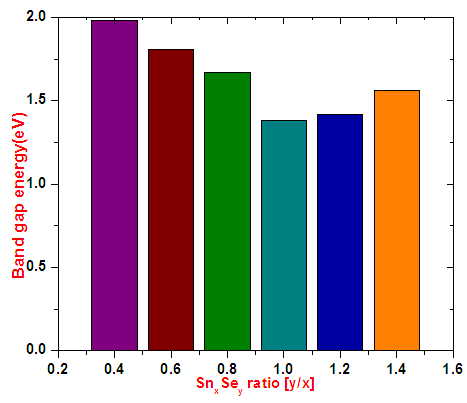 | Figure 7. Graph of variation of optical band gap energy with different Sn:Se ratios |
The refractive index of the SnxSey samples was plotted against wavelength as shown in figure 8. Refractive indices increased with increase in selenium ratio. In visible region (400-750 nm) and near infrared i.e above 750 nm the refractive index for each sample did not have significant change. This is because of low energy of the photons. Highest refractive index is at SnxSey ratio 1.0 sample. This is attributed to higher absorption which is related to the complex reflectance behaviour on the surface of the deposited thin films due to spectroscopic ellipsometry theory. 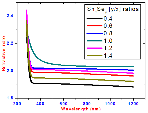 | Figure 8. Graph of refractive index (n) as a function of wavelength |
Absorption coefficient determines how far a photon of given wavelength penetrates through a material before it is absorbed. Figure 9 shows absorption coefficient for SnxSey samples. Generally all samples have absorption coefficient of 105. SnSe ratio 1.0 has the highest absorption coefficient in visible region.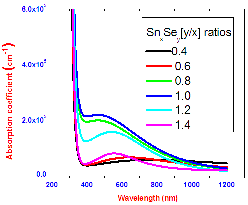 | Figure 9. Absorption coeffient for SnxSey |
At low wavelengths, absorption coefficient is high because absorption of incident photon takes place. This is because photons with lower wavelength have higher energy than the band gap hence highly absorbed. Semiconductors have a sharp edge absorption for photon with energies near the band gap. This explains the slight increase of absorption coefficients in visible region. Materials with higher absorption coefficients more readily absorb photons, which excite electrons into the conduction band [14].
3.2. Optical Properties of SnO2: Co Thin Films
Figures 10 and 11 shows the transmittance and reflectance spectra respectively. Transmittance percentage is high ranging between 70%-86% in the visible and near infra-red regions for the thin films. 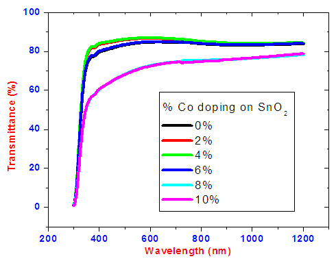 | Figure 10. Graph of transmittance spectra of cobalt doped SnO2 thin films |
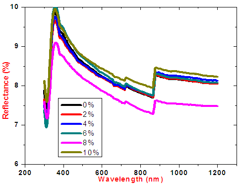 | Figure 11. Graph of reflectance spectra of Cobalt doped tin iv oxide thin films |
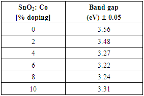
SnO2 is an oxygen deficient n-type semiconductor with a wide band gap energy  Therefore all photons with energy lower than the band gap are transmitted through the thin films with very low absorption [15]. From the spectral data, transmittance increases sharply to maximum and then remains constant for all the doped samples as the wavelength of incident photon energy increases. This is because there is minimal optical absorption that is taking place because photon energies are less than band gap of the thin films which results in lower absorption hence higher transmittance. Upon Cobalt doping transmittance increases slightly up to 4% Co doping. This can be attribute to low band edge absorption as cobalt get incorporated in host semiconductor interstitials as well as the substitution sites [16]. Reflectance is low and lie in the range of 7-10%. The maximum and minimum points formed are attributed to interband transitions where electrons from filled states at the top of valence band are excited and jump to empty states in the conduction band. These points are attained within energy range which corresponds with the energy band gap of the thin films. Table 1 shows optical band gap energy for cobalt doped SnO2. They ranged between 3.56 – 3.22 ±0.05 eV and were calculated by scout software program [17]. The band-gap energy and the transition type can also be derived from the mathematical treatment of the data obtained from the optical absorbance vs. wavelength. Tauc’s relation was used to obtain the band gap energies. Figure 12 shows how the band gap energy for 4% doped SnO2 was obtained. The band gap energies for other samples were similarly obtained.
Table 1. SnO2 doped with Cobalt and calculated band gap energy values
 |
| |
|
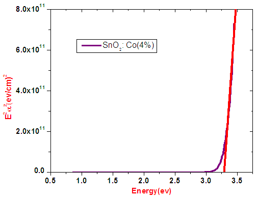 | Figure 12. Band gap energy of 4% cobalt doped SnO2 from Tauc’s relation |
Band gap energies decreased upon doping up to 6%. Decrease in band gap energy can be attributed to creation of new donor levels in the forbidden zone; and a shift in the Fermi level causing a change in the band structure of the films. Creation of new donor levels makes the electrons to jump from the maximum valence band to minimum conduction band because SnO2 is a direct band gap material [18]. The band gap energy trend shows that samples is optimized at a 4.0% doping concentration which has the highest transmittance in visible region. The increase in band gap above 6% Cobalt doping is attributed to the Burstein Moss effect. As the doping is increased carrier concentration exceeds conduction band edge density of states, which corresponds to degenerate doping in semiconductors. According to Paulli exclusion principle fermions cannot occupy same quantum state simultaneously. Therefore as doping concentration increases, more and more donor states are created in conduction band which slightly pushes Fermi level higher in energy. This in turn results into widening of the band gap.The refractive index of SnO2: Co thin films was plotted against wavelength as shown in figure 13. Samples had refractive indices range of 1.6 -1.7. Upon cobalt doping on SnO2 refractive index decreases up to 4% .This implies very low absorption and higher transmittance. Above 4% doping refractive indices are slightly higher implying more absorption. This is also attributed to changes in Fermi levels corresponding to degenerate doping.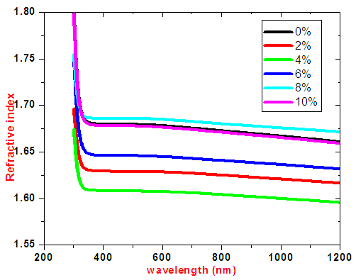 | Figure 13. Graph of refractive index against wavelength for SnO2: Co thin films |
The average extinction coefficient for all samples within the visible range were < 0.1 as shown in figure 14. As expected at low wavelengths the extinction coefficient sharply increases. This indicates that at low wavelengths, the films have very high absorption. Similarly in visible region i.e for  nm to
nm to  nm the extinction coefficient were relatively low, indicating that at higher wavelengths the material became almost transparent. A film of 2-4% doping had the lowest extinction coefficient in the visible region making it a choice for window layer for photovoltaics.
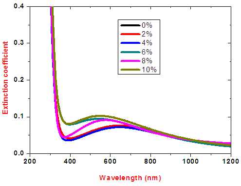 | Figure 14. Graph of extinction coefficient against wavelength for SnO2: Co thin films |
3.3. SnSe/SnO2: Co Solar Cell
Current and voltage data was obtained using a solar cell simulator fitted with dichroic reflector. Figure 15 shows the I-V characteristic of the cell. 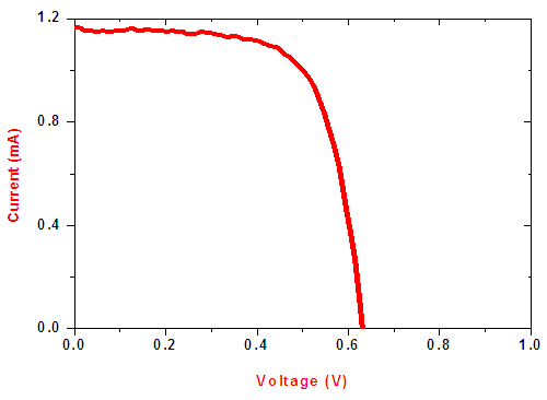 | Figure 15. I-V characteristic of the fabricated SnSe-SnO2: Co P-N solar cell |
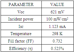
Open circuit voltage (VOC) was measured when there was no current passing through the cell, V (at I= 0) = VOC. The short circuit current (ISC) corresponds to the short circuit condition when the impedance is low and is calculated when the voltage equals zero. I (at V=0) = ISC. ISC occurs at the beginning of the forward-bias sweep and is the maximum current value in the power quadrant. Table 2 shows the parameters of the solar cell fabricated of an area 4 cm2. The open circuit voltage, VOC was 0.621 V and short circuit current, ISC was 1.12 mA. The value of short circuit current was low. This was attributed to high recombination of the charge carriers before constituting an external current. The cell had a Fill factor (FF) of 0.732. Fill factor is essentially the measure of squareness of the I-V curve. It is also calculated by comparing maximum power to the theoretical power output. The solar simulator’s incident power of 100mW per cm2 was used. The conversion efficiency (η) which is the ratio of the electrical power output, Pout to the solar power input, Pin, was 0.525%. High fill factor show that efficiency of the cell can be improved by lowering parasitic resistances and surface recombination.Table 2. Parameters of SnSe- SnO2: Co p-n junction solar cell
 |
| |
|
4. Conclusions
SnxSey films, transmittance was < 70% and reflectance <12% in the UV-VIS-NIR regions. Lower transmittance implied higher absorbance. Optimized SnxSey [y/x] sample ratio 1:1 recorded highest absorbance of 47.51%. Calculated optical band gaps of SnxSey ranged from 1.97 to 1.38 eV. SnxSey [y/x] ratio 1.0 had a lowest band gap energy of 1.38±0.05 eV. The absorption coefficient for all thin films was > 105 implying that tin selenide as a good absorber for a solar cell application. The absorption coefficient for all thin films was > 105 implying that tin selenide is a good absorber for a solar cell application. High transmittance is reported for cobalt-doped SnO2 (>80%) and low reflectance below 10% within the UV-VIS-NIR regions. The calculated optical band gaps of undoped SnO2 and cobalt doped thin films narrowed from 3.56 to 3.22±0.05 eV. Widening of the band gaps was reported above 6% cobalt doping attributed to population of states near conduction band. Cobalt doped SnO2 had lower absorption coefficients of <102. SnSe/SnO2:Co p-n junction fabricated using spray pyrolysis, the diode characteristics of p-n solar cell were obtained; short circuit current of 1.12 mA, open circuit voltage of 0.62 V, fill factor of 0.73 and a conversion efficiency of 0.525%.
ACKNOWLEDGEMENTS
The authors acknowledge Kenyatta University Physics laboratory technical staff led by Mr. Fredrick Mudimba for their technical support while carrying laboratory work. Mr. Antony Njagi technician from Chemistry Department (Kenyatta University) for his tireless assistance. We also acknowledge the technical staff of University of Nairobi Solid-State Laboratories Chiromo campus led by Mr Bonface Muthoka for their support in carrying out various measurements in their laboratory.
References
| [1] | Lewis, N.S and Nocera, D.G. (2006). Powering the planet, Chemical challenges in solar energy utilization. Proceedings of the national Academy of sciences of the United State of America, 103: 15729-15735. |
| [2] | Ohring M. (1992). The Materials Science of thin film. London. Academic Press Ltd. 79-109. |
| [3] | Bindu, K. and Nair, P. (2004). Semiconductor tin selenide thin films prepared by heating Se-Sn. Journal of Semiconductor Science and Technology, 19: 1348-1353. |
| [4] | Jorge, S.N., Manoj, R. and Dalia, M. (2012). Ultrasonic spray pyrolysis deposition of SnSe and SnSe2 using a single spray solution. Journal of Semiconductor, 1: 34. |
| [5] | Pathinettam, P., Marikani, A. and Murali, K. (2000). Optical and electrical properties of SnSe thin films for solar cell applications. Crystal Research Technology, 45: 53-58. |
| [6] | Toshiyuki, Y., Jiro, M., and Akira, Y. (1991). Thin films of CuInSe2 prepared by RF sputtering from various compositional powder targets. Solar Energy Materials and Solar Cells, 27:25-35. |
| [7] | Yinzhu, J., Yong Y., and Bahlawane, N. (2012). Abnormal behavior in electrical transport properties of cobalt doped tin oxide thin films. Journal of Materials Chemistry, 71, 213–218. |
| [8] | Subramanian, V., Jiang J.C., Smith, P.H. and ambabu, B., (2004). Preparation of Cobalt Doped SnO2. 14. |
| [9] | Pirmoradi H., J. Makootikhah, M. KarimiPour, A, AhmedPour, N, Shahtahmasebi and F, Ekhtiary Koshky (2011). Study of Cobalt-doped SnO2 thin films. Middle East Journal of Scientific Research, 8: 226-253. |
| [10] | Odari, B., Mageto, M., Musembi, R., Otieno, H., Gaitho, F. and Marimba, V. (2013). “Optical and electrical properties of Pd doped SnO2 thin films deposited by spray pyrolysis ’’ Journal of Basic and Applied Sciences, 7: 89-98. |
| [11] | Martínez-Escobar D., Manoj Ramachandran, Sánchez-Juárez A., Jorge Sergio Narro Rios, (2013). Optical and electrical properties of SnSe2 and SnSe thin films prepared by spray pyrolysis. Thin Solid Films letters, 15:59-61. |
| [12] | Kumar, N., Sharma V., Shah N., Desai M., Panchal C. and Protsenko I. (2010). Influence of the substrate temperature on the structural, optical and electrical properties of SnSe thin films prepared by thermal evaporation method. Journal of Crystal Research Technology, 1: 53-58. |
| [13] | O’Leary, J., Johnsons, R. and Lim, P. (1997). Thin film Physical models. Journal of Applied Physics. 8 (7), 12-87. |
| [14] | Poortmans, J. and Arkhipov, V. (2006). Thin film solar cells fabrication, characterization and applications. John Wiley and Sons. Chinchester. Resistance on the fill factor of a solar cell,” Solar Energy Materials a Solar Cells, 1: 277-363. |
| [15] | Subramanian, V., Jiang J.C., Smith, P.H. and ambabu, B., (2004). Preparation of Cobalt Doped SnO2. 14. |
| [16] | Yinzhu, J., Yong Y., and Bahlawane, N. (2012). Abnormal behavior in electrical transport properties of cobalt doped tin oxide thin films. Journal of Materials Chemistry, 71, 213–218. |
| [17] | W. Theiss, in: W. Theiss (Ed.), Scout Thin Film Analysis Software Handbook, Hard and Software, Aachen, Germany, 2001 www.mtheiss.com, Pg. 54-57. |
| [18] | Shadia, J., Naseem, M. and Riyad, N. (2009). Electrical and Optical properties of ZnO:Al thin films prepared by pyrolysis technique. Faculty of Science; Physics department, University of Jordan; Ammam, 11942, Jordan, 212-422. |

 Abstract
 Reference
 Full-Text PDF
 Full-text HTML