John Gitonga1, Mathew Munji1, Robinson Musembi2, Nelson Mugambi1, Geoffrey Gitonga1
1Department of Physics, Kenyatta University, Nairobi, Kenya
2Department of Physics, University of Nairobi, Nairobi, Kenya
Correspondence to: John Gitonga, Department of Physics, Kenyatta University, Nairobi, Kenya.
| Email: |  |
Copyright © 2017 Scientific & Academic Publishing. All Rights Reserved.
This work is licensed under the Creative Commons Attribution International License (CC BY).
http://creativecommons.org/licenses/by/4.0/

Abstract
Zinc Oxide was doped with various percentages of Aluminum ranging from 0% to 10% by mass. Tin (Sn) and selenium (Se) metal samples were mixed in different ratios of increasing selenium. Deposition of both SnSe and ZnO:Al thin films on glass substrate was done by a method of evaporation using Edwards Auto 306 RF/DC Magnetron evaporation system under the following conditions; deposition temperature 500K, pressure of 3.5×10⁻⁵ millibars and a current of 3.5A. Transmittance and reflectance data in the range 300nm-1500nm was obtained using a double beam solid spec 3700 UV-VIS-NIR shimadzu spectrophotometer. Doping of 5% aluminium and a synthesized ratio of 1:1.0 for ZnO:Al and SnSe thin films respectively was obtained as the optimum values. The optimized Al doped ZnO was deposited at different deposition temperature ranging from 350K-550K. Transmittance percentage in the visible region was used to optimize deposition temperature and 510K was obtained as the optimum value. Band gap energies of optimized ZnO:Al and SnxSey was found to be 3.61±0.05 eV and 1.37±0.05 eV respectively.
Keywords:
Resistive Evaporation, Zinc Oxide, Tin, Selenium, Deposition Temperature
Cite this paper: John Gitonga, Mathew Munji, Robinson Musembi, Nelson Mugambi, Geoffrey Gitonga, Effect of Substrate Temperature on the Optical Properties of SnxSey/ZnO:Al P-N Junction Solar Cell, American Journal of Materials Science, Vol. 7 No. 6, 2017, pp. 250-257. doi: 10.5923/j.materials.20170706.04.
1. Introduction
The technologies applied in the manufacture of solar cells is wide with thin film technology being commonly applied as it ensures charges generated have short diffusion length, quantity of material used is relatively small and the cell has high charge recombination rate [1]. Modern electrical devices have been developed from transparent conducting oxide (TCO) films made using binary compounds such as In2O3, ZnO and SnO2 which have been doped [2]. ZnO form very strong chemical bonding which makes them behave like semiconductors with a wide band gap [3, 4]. These oxides have been used in polycrystalline industries and thin film technology [3, 5] e.g. solar cells, gas sensors, optoelectronic devices and electromagnetic shielding functional glasses. ZnO have been used as heat-efficiency windows in refrigerators and air planes by reflecting in infrared while remaining transparent in the visible region [6]. From the documented results, the best n-type TCOs are Aluminium-doped Zinc Oxide (ZnO: Al), Niobium-doped Titanium Oxide (TiO:Nb), Tin-doped Indium Trioxide (In2O3: Sn) and Fluorine-doped Tin dioxide (SnO2: F) thin films [7, 8]. Optical transparency of more than 90% has been obtained in these films [9, 10]. Samples coated with ZnO:Al show little degradation and have very good solar cell properties [11]. The optical, electrical and structural properties of ZnO:Al heavily depended on deposition parameters [12]. These advantages informed the choice of ZnO:Al as the window layer of the solar cell in this study.The AZO thin films have been prepared by various methods such as sol-gel processing [13], magnetron sputtering [14], and CVD [15]. Resistive evaporation method is most suitable for preparation of thin films where deposition parameters such as deposition temperature, film thickness and pressure were to be highly controlled [16]. In this study, resistive evaporation method was used. It is where materials from a thermal vaporization source reaches the substrate with little or no collision with gas molecules in the space between the source and substrate. The gaseous atoms are transported to the substrate surface in reduced pressure environment [17]. The vacuum environment during evaporation provides the ability to reduce gaseous contamination in the deposition system to a low level. This technique is generally done using thermally heated sources such as tungsten wire coils or by high energy electron beam heating of the source material itself. The main purpose of this study was to improve the efficiency of the Tin Selenide Aluminum doped zinc oxide junction solar cell. This was achieved by fabricating the solar cell using optimized deposition parameters.
2. Experimental
2.1. Sample Preparation
2.1.1. Tin Selenide (SnxSey)
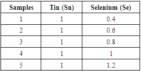
Tin and selenium which are group four and group six elements were used to make the P- layer. Tin (99%) purity and selenium (99.5%) purity samples were synthesized in specific ratios by mass ranging from 0.4 to 1.2 as shown in table 1. The mixer was melted in a Pyrex glass-tube in the presence of argon (Ar) gas flowing at 20sccm to avoid oxidation. The glass container was heated in an oven to a temperature of 623 K until the two materials melted and mixed evenly. The heating was done continuously and gently to prevent the glass from breaking. The glass tube was completely sealed and its content allowed to cool down to room temperature (298 K) before removing the mixture. The mixture was then cut into ingots that were used in the next step of thin film deposition. Table 1. Tin selenide samples showing various tin to selenium ratios
 |
| |
|
2.1.2. Aluminium Doped Zinc Oxide (ZnO:Al)
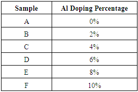
Aluminum (99.99% purity) and Zinc (99.9% purity) were mixed at varying doping percentages of Aluminum in the range (0 – 10%). The values of doping percentages were arrived at by calculations from the relative molecular mass of the compound. The various samples that were made are shown in table 2 below. Samples were put in a silica glass tubes and then heated in presence of a constant flow of argon gas in a glass tube to form a homogenous compound. The resulting alloy was cooled naturally to room temperature forming ingots.Table 2. Zinc oxide sample showing various aluminium doping percentage
 |
| |
|
2.2. Thin Films Deposition
2.2.1. SnxSey Thin Films
The thin films were prepared using resistive evaporation method in an Edwards vacuum deposition setup model Auto 306. The Auto 306 uses a turbo molecular pump and it’s fully automatic in its pumping procedures. The pressure is monitored using a compact gauge capable of recording atmospheric to sub-atmospheric pressure [16] Figure 1 shows a photo Edwards Auto 306 used in this study. | Figure 1. Edwards Auto 306 coating unit |
The compound was ground in a porcelain motor, and placed in an evaporator boat in a vacuum chamber. Heat was supplied to the boat at a current of 3.5 A. Glass slides made measuring 150 mm × 400 mm were used as substrates. They were cleaned to remove any trace of stains using distilled water and ethanol and allowed to dry completely. A glass substrate would be mounted on a substrate holder by clips and the shutter directly overhead removed to allow deposition. Films were deposited at a substrate temperature of 500 K. Current of 3.5 A was set to flow through the substrate holder and temperature changes noted from the thermocouple.
2.2.2. ZnO:Al Thin Films
Evaporation technique was used to deposit the thin films. The thin films were produced in Edwards 306 vacuum coater. Glass slides were used as substrate for depositing the thin films. They were cleaned to remove any trace of stains using distilled water and ethanol and allowed to dry completely. The substrate was then mounted on a rotating substrate holder. The compound was ground in a porcelain motor and placed in an evaporator boat in a vacuum chamber. The chamber was covered tightly and pumped down to 3.0 x 10⁻⁵ mbars. A current of 4.5 A was supplied to the heater to evaporate the materials. A current of 3.5 A was allowed to the substrate holder to attain a deposition temperature of 500 K. The shutter was removed to permit deposition on glass substrate in the presence of oxygen which was let into the chamber. Since Zinc is more reactive than Aluminum, ZnO:Al thin films were formed. The Bond enthalpy of Zn-O is 159±4 kJ/mol while that of Al-O is 511±3 kJ/mol [18]. After optimizing the doping percentage, samples with an optimum value of 5% aluminium were deposited at different deposition temperature ranging from 350 K-550 K.
2.2.3. SnSe-ZnO:Al Heterojunction Fabrication
Fabrication of SnSe-ZnO:Al heterojunction solar cell was done in stages. Reactive evaporation technique was employed in the deposition. The window layer, aluminium doped zinc oxide was first deposited in the glass slide using the following depositions parameters; deposition temperature of 510 K, chamber pressure of 3.5×10⁻⁵ millibars and a substrate distance of 12 cm. Then the absorber layer which is SnSe was deposited on the ZnO:Al at a deposition temperature of 500 K. Finally a back contact of aluminium coat was made on the SnSe film to obtain the p-n heterojunction.
2.3. Optical Characterization
Optical measurements (reflectance and transmittance) in the spectral range from 300 nm - 1500 nm were carried out using UV/VIS/NIR 3700 double beam Shimanzu spectrophotometer. Photons of selected wavelengths and beam intensity Io (photons/cm2-s) were directed at the film of thickness (t) and their relative transmissions observed. Wavelengths of photon are selected by the spectrophotometer. Photons with energies greater than band gap (Eg) are absorbed while those with energies less than Eg are transmitted. Figure 2 below shows a photograph of spectrophotometer used in this research. The spectrophotometer had two radiation sources; a deuterium lamp for UV range and a halogen lamp for visible (VIS) and near infrared (NIR) range. The radiation source changed automatically to access the wavelength range during measurements. During transmission measurements, samples were placed in front of the integration sphere and behind it during reflection measurements. Proprietary software SCOUT 2.4 was used in analyzing the collected data in order to determine thickness (t) of thin films, extinction coefficient (k) and the refractive index (η). [19]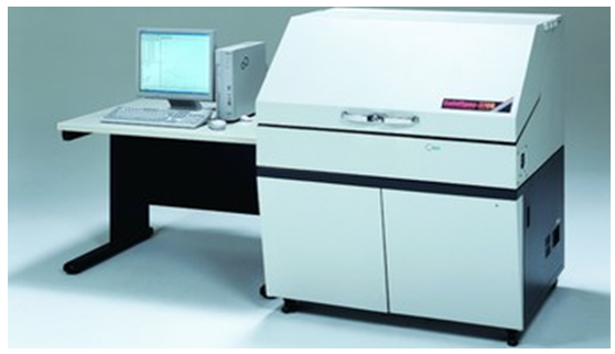 | Figure 2. The UV-VIS-NIR Spectrophotometer 3700 DUV (Shimadzu) |
3. Results and Discussion
3.1. Optical Characteristics of ZnO:Al
3.1.1. Optical Spectra of ZnO:Al Thin Films
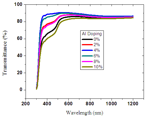 | Figure 3. Graph of transmittance spectra of ZnO:Al films |
The optical transmittance spectra of ZnO:Al films as a function of wavelength in the range (300 - 1200 nm) were plotted. Figure 3 above shows different spectra for films with different aluminium doping percentages. High values of transmittance ranging from 60% to 90% were obtained as shown in the figure above. Transmittance increased steadily to a maximum value before remaining constant as the wavelength increases for all the samples. This can be attributed to minimal optical absorption taking place as the energies of the incoming photons are lower than the band gap energy of the thin films. As the doping percentage was increased beyond 5%, there was a slight decrease in transmittance. This is due to excess free carriers coupling to the electric field hence increasing the reflection. This agrees very well with [20] who reported significantly reduced transmission when ZnO was doped with higher percentages of Aluminum. Average transmittance for different spectrum region was calculated and a high transmittance of 80.76% was recorded in the visible region as shown in table 3 below.Table 3. Average transmittance of ZnO:Al within different spectrum regions
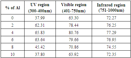 |
| |
|
Figure 4 below shows a graph of average transmittance with aluminum doping in the visible region. As the aluminum percentage was increased, transmittance increased up to 5% beyond which a decreased was observed. At 5% doping, samples attain crystalline nature which allows maximum photons to pass through. This can also be attributed to improved surface morphology which reduces reflection of normal incident photons at this percentage as shown in figure 5 below.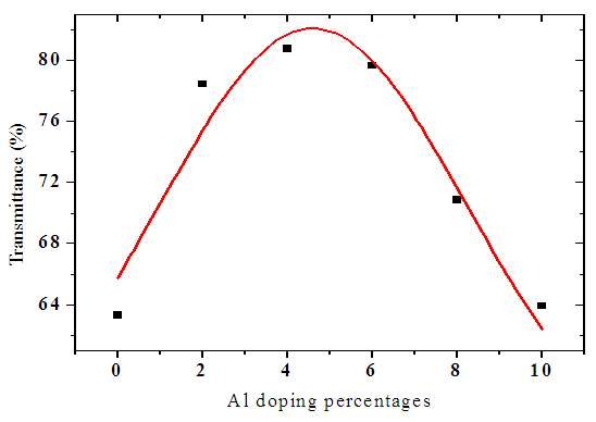 | Figure 4. Graph of average transmittance in ZnO:Al within the visible region |
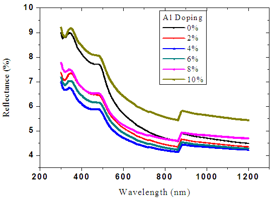 | Figure 5. Graph of reflectance spectra of ZnO:Al films due to doping |
Very low values reflectance ranging from 4% to 9% in the ultra violet, visible range and infra-red was recorded. Figure 5 above shows the nature of spectra scattered from the reflectance data. The kinks observed in the spectra was due to spectrophotometer changing radiation source from either a halogen lamp for visible (VIS) and near infrared (NIR) range or a deuterium lamp for UV range. This occurs automatically in order to access the wavelength range during measurements as deposition temperature was increased.The values of transmittance increased with increase in deposition temperature as shown in figure 6 below. A high value of more than 86% was recorded in the visible light. This is because increase in deposition temperatures reduced the size of crystalline [21]. The cleavage network was increased hence the amount of photons passing increases. Also at higher deposition temperature, the aluminium ions tend to occupy substitutional site as compared to interstitial site. This ensures little crystal defects hence minimal blockage of photons which lead to higher transmission.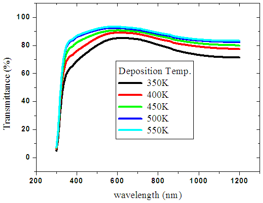 | Figure 6. Graph of reflectance spectra of ZnO:Al films due to deposition temperature |
3.1.2. Optical Band Gap Energies
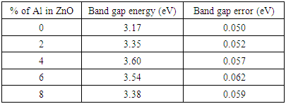
Table 4 below shows variation of aluminium doping percentages and their corresponding optical band gap energy. The obtained optical band gap lies from 3.17-3.60±0.05 eV. The slight increase in band gap energy from 3.17 eV to 3.60 eV can be attributed to Burstein moss effect. When doping concentration is increased, all states near the conduction band are populated. The fermi energy level is pushed higher hence increasing the band gap energy. When the doping was increased beyond five percentages, there was slight decrease in band gap energy. This can be attributed to creation of new donor levels above the valence band. Table 4. ZnO doped with aluminium and calculated band gap energy values
 |
| |
|
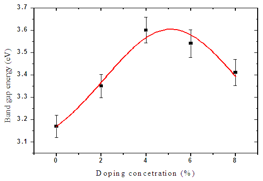 | Figure 7. Graph of band gap energy with doping concentration |
By use of Gaussian amplified peak function, doping percentage was optimized at 5% aluminium doping as shown in figure 7 above with a band gap of 3.60 eV. The 5% was used in the solar cell fabrication. This value falls within the range of 3.28-4.20±0.05 eV reported by [22].Figure 8 below shows variation of band gap for the window layer with deposition temperature. There was a slight increase in band gap from 3.60eV to 3.61eV. Which can be due to the increase in thin films thicknesses with increasing the substrate temperature.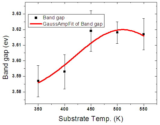 | Figure 8. Graph of band gap energy with deposition temperature |
3.1.3. Thickness of the ZnO:Al Thin Film
The figure 9 below shows variation of film thickness (nm) with increase in deposition temperature. The thickness decreased exponentially as there was a high rate of re-evaporation at high deposition temperature on the glass substrate. At higher deposition temperature, most atoms on the outer layer moves very fast to occupy site of lowest binding energy hence forming a low energy structure. This kind of a surface has a uniform crystal arrangement making the surface smoother and uniform.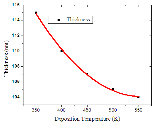 | Figure 9. Graph of film thickness with deposition temperature |
3.2. Optical Characteristics of SnSe
3.2.1. Transmittance Data against Wavelength
The transmittance of all synthesized ratios of tin selenide was observed to be below 40% as shown in figure 10 below. The values agree with a transmittance of below 45% reported by [23]. It is observed that there is variation in transmittance within the visible region due to variation in selenium ratio. There was a slight decrease in transmittance for wavelengths above 600 nm. This can be attributed to increase in optical scattering caused by rough surface morphology. As the ratio of selenium was increased, transmittance decreased. Beyond the ratio of 1:1, there was slight increase in transmittance which can be attributed to structure deformity. A SEM machine with high resolution should be used to study the homogeneity of the bonding. The ratio of 1:1 gave the lowest transmittance in the visible region. This makes the material suitable candidate for application as absorber electrode for solar cell.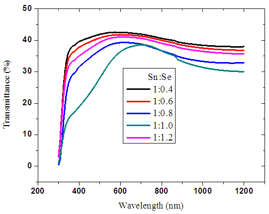 | Figure 10. Graph of transmittance spectra of SnxSey thin films deposited at 500 K |
3.2.2. Transmittance, Reflectance and Absorbance Averages in the Visible Region
The values of absorbance in the visible region were noted to be above 50% as shown in figure 11 below. There was a slight increase in absorbance as the ratio of selenium was increased in the mixture. Much of the incoming photons have energies comparable with the band gap of the material. This leads to an increase in absorption. A ratio of 1:1 gave a higher absorbance of 58.93% in this region of spectrum. This value was used as optimum synthesis ratio in the fabrication of the p-n solar cell junction.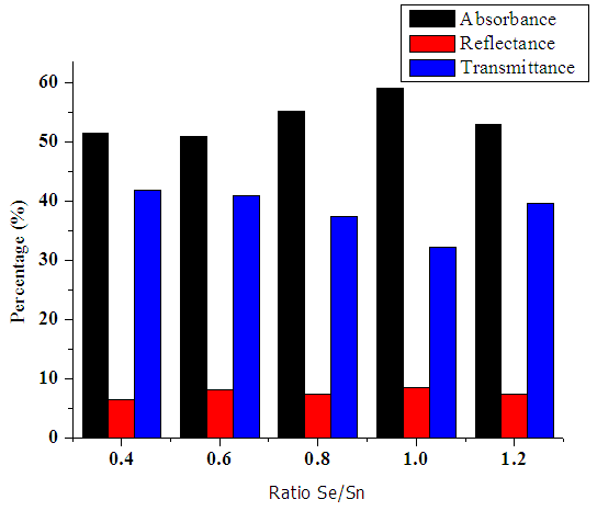 | Figure 11. Graph of transmittance, absorbance and reflectance in visible region |
3.2.3. Optical Band Gap Energies
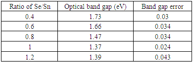
The band gap energy values were obtained by the SCOUT 2.4 software that was used in simulation. The thickness of the thin films as calculated by the SCOUT 2.4 software was found to lie between 104.14 and 115.12±0.1 nm. Table 5 below shows the optical band gap energy for different ratios of Sn:Se thin film samples. The optical band gap energy lies between 1.37 and 1.73±0.05 eV with the Sn:Se ratio of 1:1 having the lowest band gap energy as shown in table 5 below. The absorption of incoming photons takes place at the top of the valence band. Excited photons have sufficient energy to overcome the potential barrier due to forbidden zone and cross over to the bottom of the conduction band. SnSe thin films exhibit direct optical energy band gap. Obtained values are in good agreement with the band gap value range of 1.18 and 1.85±0.05 eV as reported by [24].Table 5. Band gap energy values and ratios of Se/Sn by mass
 |
| |
|
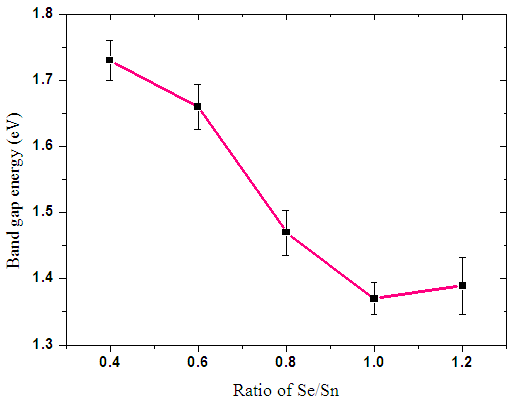 | Figure 12. Graph of variation of optical band gap energy with different Sn:Se ratios |
From the results, a graph of optical band gap energy versus Se/Sn sample ratios was drawn. The variation in graph shows that the optimum Sn:Se thin film ratio value is that of 1:1 since it had the lowest energy band gap value of 1.37±0.024 eV as shown in the figure 12 above. From the table above it is evident that the optical band gap decreases as the concentration of tin in the alloy is increased in the as-deposited films. This can be attributed to formation of new structural units with lower optical threshold energy whose presence may contribute to lowering of the mean value of band gap in the alloys.
3.2.4. Thickness of the SnSe Thin Films
The thin film was deposited at optimised temperature of 500K. This gave the absorber layer a uniform thickness of 103 nm. Since temperature is a measure of the average kinetic energy of a system of particles, as temperature increases the film particles gain more kinetic energy to move thereby reducing mass transport to the substrate. Deposition at this temperature offered a thickness which ensured minimal recombination of photons.
3.2.5. Refractive Index
Refractive index values of SnxSey samples were plotted against wavelength as shown below. 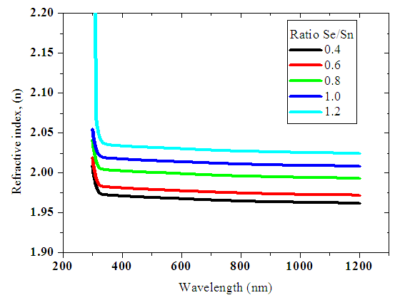 | Figure 13. Graph of refractive index (n) as a function of wavelength |
Figure 13 above shows that the refractive indices of the thin films remain fairly constant as the wavelength increases. This must be related to the complex reflectance behavior on the surface of the deposited thin films. This is attributed to spectroscopic ellipsometry theory; which defines the ability to report real refractive index of thin films over a wide range of wavelength values.
3.2.6. Absorption Coefficient for Tin Selenide
Absorption coefficient for tin selenide at different ratios was plotted against wavelength from 300 nm to 1200 nm. A sample with a ratio of 1:1.0 recorded the lowest absorption coefficient as shown in figure 14 below. For all samples, tin selenide had a low absorption coefficient within the visible range (380-750 nm) with an average absorption of more than 2.0 × 105 cm-1. This makes it reliable material for use as a absorber layer for solar cells. [25].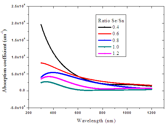 | Figure 14. The absorption coefficient against wavelength for tin selenide |
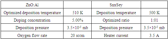
3.3. Optimized Deposition Parameters of ZnO:Al and SnxSey Thin Films
Table 6 below gives the optimized deposition parameters for different doped concentrations of ZnO:Al thin films and varied synthesized ratios of SnxSey. These parameters were used in the fabrication of PN junction solar cell.Table 6. Optimized deposition parameters for ZnO:Al and SnxSey thin films
 |
| |
|
4. Conclusions
Window layer samples registered higher transmittance in the range of 60-90%. This was primarily due to minimal optical absorption as the doping increased the band gap. Excess doping reduces transmittance as these free charge carriers couples with electric field hence increasing the reflections. Samples deposited at optimized temperature exhibited a higher transmittance. This is because the thin films formed had reduced and uniform crystalline structure. Their optical band gap ranged from 3.17eV-3.60eV with increase in doping percentage. There was a slight increase in band gap to 3.62eV when the sample was deposited at optimized temperature.
ACKNOWLEDGEMENTS
The authors of this paper would wish to acknowledge the technical staff of both Kenyatta and Nairobi University in Particular joachm njagi and Boniface muthoka for their technical advice while carrying out the experiments in the Laboratory.
References
| [1] | Fuller, C.S. Chapin, D.M. and Pearson, G.L. (1954). A new silicon p-n junction photocell for converting solar radiation into electrical power. Journal of Applied Physics, 25: 676-678. |
| [2] | Tadatsugu M, Takashi Y, Yukinobu T, Toshihiro M. Transparent conducting zinc-co-doped ITO films prepared by magnetron sputtering. Thin Solid Films. 2000; 373: 189-194. |
| [3] | Mohammad-Mehdi B. and Mehrdad S., J. Phys. D: Appl. Phys 37 (2004) 1248-1253. |
| [4] | Maghanga C.M., Jensen. J., Niklasson G.A., Granqvist C.G., Mwamburi M.M. (2010). Transparent and Conducting TiO2:Nb films made by Sputter Deposition 94: 75-79. |
| [5] | Roos, A. and Georgson M. (1991). Material Science for Solar Energy Conversion Systems. Materials Science and Engineering, 22: 29. |
| [6] | Walsh A. (2011). Semiconducting Oxides, Physics of condensed matter, 23:334210. |
| [7] | Mageto J.M., Mwamburi M.M. Muramba V. W., (2012). The influence of Al doping on optical, electrical and structural properties of transparent and conducting SnO:Al thin films prepared by spray pyrolysis technique, Elixir Chemical Physics 53: 11922-11927. |
| [8] | Muramba V. W., (2013). Preparation and Characterization of Transparent and Conducting Doped Tin Oxide Films; Masters thesis. |
| [9] | Lewis B.G and Paine D.C (2000). MRS Bull. Size-dependent Electrical Behavior of Spatially Inhomogeneous Barrier height region on Silcon. Applied Physics 77:2566-2568. |
| [10] | Gordon R.G and Bright C (2000). Highly Transparent and conductive thin films of ZnO doped with a rare-earth element; Thin Solid Films 25: 52. |
| [11] | Zhao, Y., Xinhua, G and Wang, W. (2002). Research and development Activities of silicon-based thin film solar cells in China. Thin film Devices and Technology, 203: 25-35. |
| [12] | Tang N., Tomoyuki K. and Takahiro M. (2000). Thin film solar cell with ZnO Buffer layers. Journal of Applied Physics, 37: 499-501. |
| [13] | Y. Takahashi, Y. Wade, J. Eletrochem. Soc. 127 (1990) 267. |
| [14] | B.S. Chiou, S.T. Hsieh, W.F. Wu, J. Am Ceram. Soc. 77 (1994) 1740. |
| [15] | G. Sanon, A. Rajrup, Mansingh, Thin Solid Films 190 (1990) 287. |
| [16] | Chapin, D. M., Fuller. C.S., and Pearson. G.L. (1954). A new silicon p-n junction photocell for converting solar radiation into electrical power. Journal of Applied Physics, 25: 676-678. |
| [17] | Ohring, M. (1992). The Materials Science of thin films. London. Academic Press Ltd, 79-109. |
| [18] | Atanas, T. and Verka, G. (2010). Optical and electrical properties of nanocrystal zinc oxide films prepared by dc magnetron sputtering at different sputtering pressures. Applied Surface Science vol, 19964-19965. |
| [19] | Theiss, W. (2000). Scout thin films analysis software handbook, edited by Theiss M (Hand and Software Aachen German) www.mtheiss.com. |
| [20] | Elmin, B., Serdar A., Salih Y., Mehmet P. and Mustafa A. (2009). Structural, optical and electrical properties of Al-doped ZnO microrods prepared by spray pyrolysis. Thin Solid Films, 133: 245–253. |
| [21] | O’Donnell K. P. and X. Chen (1991). Temperature dependence of semiconductor band gaps. Journal of Applied Physics, 58 (25): 4-5. |
| [22] | Mugah C. O., (2011). Characterization of SnSe/ZnO:Al P-N junction for solar cell application. M.sc. (physics) Thesis. Kenyatta University, Kenya. |
| [23] | Kioko, L. M., (2011). Characterization of SnSe/ZnO:Sn P-N junction for solar cell application. M.sc. (physics) Thesis. Kenyatta University, Kenya. |
| [24] | Kumar, N., Sharma, V., Shah, N., Desai, M., Panchal, C. and Protsenko, I. (2010). Influence of the substrate temperature on the structural, optical and electrical properties of SnSe thin films prepared by thermal evaporation method. Journal of Crystal Research Technology, 45 (1): 53-58. |
| [25] | Porortmans, J. and Arkhipov, V. (2006). Thin film solar cells fabrication, characterization and applications. John Wiley and Sons. Chinchester. |

 Abstract
 Reference
 Full-Text PDF
 Full-text HTML