-
Paper Information
- Paper Submission
-
Journal Information
- About This Journal
- Editorial Board
- Current Issue
- Archive
- Author Guidelines
- Contact Us
American Journal of Materials Science
p-ISSN: 2162-9382 e-ISSN: 2162-8424
2017; 7(6): 240-249
doi:10.5923/j.materials.20170706.03

Optical Characterization of SnxSey: SnO2-Ni Prepared by Spray Pyrolysis for Photovoltaic Application
 Abstract
 Reference
 Full-Text PDF
 Full-text HTML
Nelson Mugambi1, Mathew Munji1, Robinson Musembi2, John Gitonga1, Geoffrey Gitonga1
1Department of Physics, Kenyatta University, Nairobi, Kenya
2Department of Physics, University of Nairobi, Nairobi, Kenya
Correspondence to: Nelson Mugambi, Department of Physics, Kenyatta University, Nairobi, Kenya.
| Email: |  |
Copyright © 2017 Scientific & Academic Publishing. All Rights Reserved.
This work is licensed under the Creative Commons Attribution International License (CC BY).
http://creativecommons.org/licenses/by/4.0/

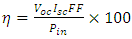
Nickel doped tin oxide and tin monoselenide thin films were coated using spray pyrolysis on glass substrate at 375°C. Nickel doped tin oxide Precursor solution was prepared using Tin (II) Chloride (SnCl4.2H2O) and uniform concentration of (NiCl2.6H2O) of 0-10%. Precursor solution of tin selenide was prepared using alcoholic solution consisting of tin chloride (Sncl2.2H2O) and 1, 1-dimethl-2-selenourea (C3H8N2Se). Samples of (SnxSey) were made in ratios of 1:0.4 to 1:1.4. The samples of tin selenide and Nickel doped tin oxide were characterized by measuring their optical properties using UV-VIS-NIR spectrophotometer 3700 DUV. The optical band gap of deposited tin selenide ranged between 1.39-2.23ev. The sample of Sn:Se1.0 had the highest absorbance of over 46.26% and lowest transmittance of about 44.3% in the VIS-NIR region. The optical band gap of deposited Nickel doped tin oxide ranged between 3.65-3.75ev. The sample of Nickel doped tin oxide of 2% concentration had the highest transmittance of 86.2% and lowest absorbance of about 5.05% in the VIS-NIR region. These properties are suitable for window and absorber layers for application in photovoltaic cell. A conversion coefficient (η) of 0.4609% was obtained for Tin selenide (SnxSey) and nickel doped tin oxide (SnO2: Ni) Solar cell.
Keywords: Spray Pyrolysis, Tin oxide, Ni-doping, Selenide, Deposition temperature
Cite this paper: Nelson Mugambi, Mathew Munji, Robinson Musembi, John Gitonga, Geoffrey Gitonga, Optical Characterization of SnxSey: SnO2-Ni Prepared by Spray Pyrolysis for Photovoltaic Application, American Journal of Materials Science, Vol. 7 No. 6, 2017, pp. 240-249. doi: 10.5923/j.materials.20170706.03.
Article Outline
1. Introduction
- Energy is the main driver in any economy, because advancement in technology is directly or indirectly related to energy. Consumption of energy has steadily raised with sophistication of the world. Presently, growing concern is in venture of Photovoltaic cells which are inexpensive rather than major energy sources (fossil fuels) whose cost is ever increasing. Increase in petroleum prices have been contributed by the increase in demand due to human population causing upward pressure [19, 12].The Silicon-based solar cell is principally used in photovoltaic industry. Silicon as an absorber material is limited because of its indirect band gap as compared to direct band gap materials [5]. The main advantage of thin film solar cells in comparison to silicon solar cells is that less energy is needed for processing, comparatively lower costs of the materials needed thus large scale production [30, 16]. SnSe is a group IV-VI semiconductor thin film having a wide range of applications due to its high absorption and suitability for optoelectronic applications because it has a narrow direct band gap energy which is around 1.1eV [6, 2, 15, 9, 10, 11, 14]. SnSe2 thin films were obtained in the substrate temperature range from 270°C to 300°C. At 270°C SnSe2 forms acceptable values of resistivity and mobility. The result obtained indicates the possibility to use these materials in a photovoltaic structure built completely by Ultra sonic Spray Pyrolysis technique [7, 18].SnO2 in its pure form has a wide band of approximately 3.7 eV and therefore a better n type semiconductor [27]. Pure SnO2 film is inferior electrical conductor that is exceedingly transparent in the visible light. However their poor electrical conductivity can be improved by doping with impurities or controlling the stoichiometry [24, 29]. Doping tin dioxide by Fe, Co, Ni, and Cu (0–16 at %) has revealed that the dopants promote both the change of the film morphology and the decrease of grain size on the conducted research during the spray pyrolysis deposition. The doping influence on both the film morphology and the grain size is weakened at higher pyrolysis temperatures 450°C [8]. SnO2 doped with Nickel powder samples with dopant concentrations in the range of 3 at % to 15 at % were prepared using solid-state reaction. A decrease in optical band gap was revealed with the rise of Ni doping levels [13, 22, 28]. When light is illuminated on a semiconductor, intensity of transmission, absorption and reflection can be measured. A lot of information such as band gap of the material can be obtained pertaining a semiconductor from these optical effects [21]. Optical radiation is absorbed by excitation from one energy level to a higher energy level in semiconductors on condition that energy of radiation
 is same to or more than the distinct in energy between the two participating levels. Transmittance through the film of thickness (d) and the intensity of radiation I dependence is of the form:
  | (1) |
 | (2) |
 | (3) |
 | (4) |
 | (5) |
 | (6) |
 | (7) |
 is the frequency, whereas β takes the value of probable 1 or 4. β gives the transition kind whichever can be direct transition or indirect transition between the semiconductor states. For instance when
  against the photon energy
  is plotted, and the linear graph which cuts the photon energy
  axis gives the direct band gap value [30]. Scout software 32 bit software for windows 98/NT/2000/XP/Vista was used for the analysis and simulations of optical spectra such as absorbance, Attenuated total reflection (ATR), reflectance, transmittance, ellipsomery, and electroluminescence [25].In this report we present reflectance, absorbance and transmittance measurements of SnSe and Nickel doped Tin Oxide on glass substrates prepared by spray pyrolysis and fabrication of p-n junction solar cell with glass/SnO2: Ni/SnSe/Al.
2. Experimental
2.1. Sample Preparation and Deposition
- Precursor solution was prepared using a 0.05M Tin (II) Chloride (SnCl4.2H2O) mixed with 0.05 M Nickel chloride 6-hydrate (NiCl2.6H2O) in distilled water and ethanol in the ratio 1:1 to get equal proportions. The solution was left for a week for complete dissolution. Molar masses were used to calculate the percentage of dopant in SnO2: Ni solution. Spray pyrolysis deposition conditions for the films were; substrate temperature of 375°C, rate of flow 6ml/min, air carrier gas of pressure 4.5 × 10⁵ Pa, Nozzle-Substrate height of 20cm. Tin monoselenide was prepared using precursor compounds which include 0.05M 1, 1-dimethyl-2-selenourea (C3H8N2Se) compounds and 0.05M SnCl2.2H2O mixed with distilled water and isopropyl alcohol in a ratio of 1:3. Molar masses were used to calculate the ratios of SnxSey. The ratios were 0.4, 0.6, 0.8, 1.0, 1.2, and 1.4. Thin films with different ratios of Selenium were fabricated on a microscope glass substrate. The deposition conditions for the films were; substrate temperature of 375°C, solution flow rate of 8ml/min, argon carrier gas of pressure 4.5 × 10⁵ Pa, Nozzle-Substrate height of 20cm.Deposition of the thin films was done using the spray pyrolysis technique as shown in figure 1. To produce SnO2, Ni: SnO2, SnxSey and SnxSey: Ni-SnO2 films, the solution was sprayed onto a pre-heated normal microscope glass substrate using compressed air for the atomization of the precursor. At the heated surface, different types of ions in thermal motion are attracted or repelled under the action of electric forces. The more stable chemical composites are crystallized on the substrate forming a thin layer.
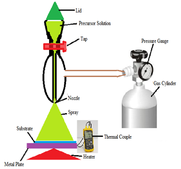 | Figure 1. Spray Pyrolysis Setup |
 | Figure 2. Schematic diagram of SnSe-SnO2: Ni p-n Junction |
3. Results and Discussion
- 3700 DUV UV-VIS-NIR Spectrophotometer was used to obtain the experimental data for transmittance and reflectance using the software of UV probe. Microsoft excel converted the data in its format from which spectra graphs were plotted separately for both tin selenide and Nickel doped Tin Oxide thin films using Microcal Origin 8.
3.1. Tin-Selenide (SnxSey)
3.1.1. Transmittance Spectra of Tin Selenide (SnxSey) Thin Films
- The transmittance spectra for SnxSey samples at different Tin to Selenium ratios is shown on Figure 3. The graphs shows that transmittance were below 65% in the visible range (400nm-780nm). As wavelength of incident photon increases, it was observed that transmittance also increased. This was due to low absorption as a result of energy of photons being lower than the band gap.
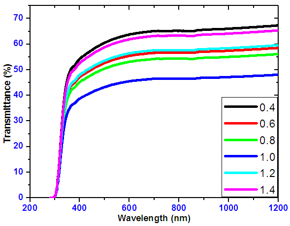 | Figure 3. Transmittance spectra against wavelength for SnxSey in various ratios |
3.1.2. Reflectance Spectra for Tin Selenide (SnxSey) Thin Films
- Spectra of optical reflectance for tin selenide is shown in Figure 4. The graph shows that the reflectance within the visible region was less than 10% for all the samples. This indicates that the films had high absorption and thus can make them good absorber layer for photovoltaics.
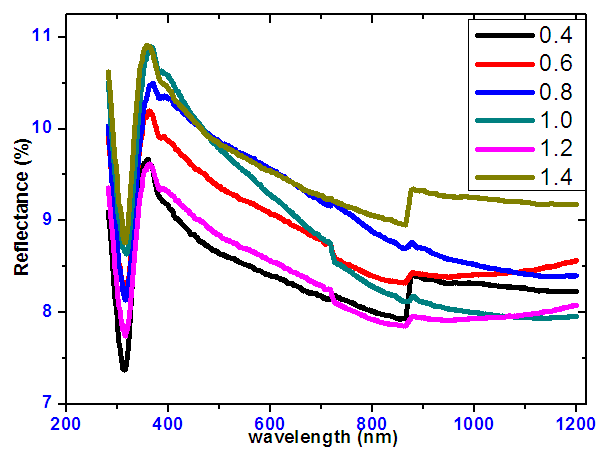 | Figure 4. Optical reflectance spectra of tin selenide in various ratios |
3.1.3. Absorbance Spectra for Tin Selenide (SnxSey) Thin Films
- Figure 5 shows spectra of optical absorbance of tin selenide. The absorbance decreases with increase in wavelength. At lower wavelengths the photons has high energy compared to the band gap energy hence a lot of it is absorbed. SnSe ratio of 1:1 has the highest absorbance in VIS region.
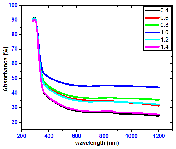 | Figure 5. Optical absorbance spectra of tin selenide in various ratios |
3.1.4. Absorption Coefficient for Tin Selenide (SnxSey) Thin Films
- Absorption coefficients at different ratios for tin selenide with varying wavelength from 280 nm to 1200 nm is shown on figure 6. From the curves, at lower wavelengths high absorption coefficients were obtained for the different tin-selenium samples. For all the samples the average absorption coefficient within the visible range (400-780) nm increases with increasing tin-selenium ratio up to a ratio 1:1 and then decreases. The Sn:Se gave an average absorption coefficient > 105 cm-1 thus making it a dependable material for casting a good absorber layer for solar cells [20]. Electrons in the valence band absorbs the photons hence excited into the conduction band.
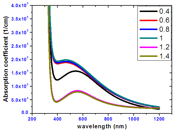 | Figure 6. The absorption coefficient for different tin selenide ratios versus wavelength |
3.1.5. Extinction Coefficient for Tin Selenide (SnxSey) Thin Films
- Figure 7 shows the extinction coefficient against wavelength. As the tin selenide ratios increases, extinction coefficient increases. The film of ratio 1:1 recorded the highest extinction coefficient, this implies that its rate of absorption is good.
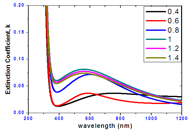 | Figure 7. Extinction coefficient against wavelength of SnSe thin films for various tin selenide ratios |
3.1.6. Refractive Index for Tin Selenide (SnxSey) Thin Films
- The variation of refractive index of SnxSey thin films against wavelengths is shown on figure 8. As wavelength increases, it is observed that the refractive index decreases. Important to note is that a ratio of SnSe as the highest refractive index implying that it is a good absorber material this is because the radiation takes a longer time through the film using.
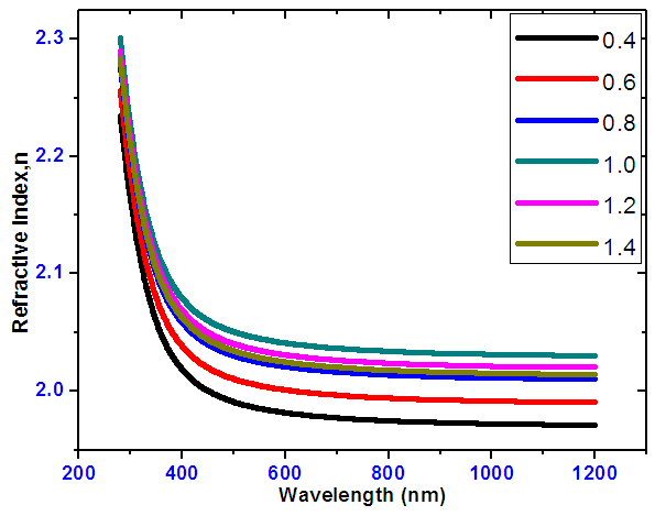 | Figure 8. Refractive index versus wavelength of SnSe of varying ratios |
 | (8) |
3.1.7. Averages of Transmittance, Absorbance and Reflectance in VIS Region of SnxSey
- Figure 9 shows how averages of transmittance, absorbance and reflectance of SnSe thin films varied with SnxSey ratios within visible region. It is clearly seen a sample of ratio1:1 has the highest absorbance. The average transmittance for all the samples in VIS region was below 65%, reflectance for all the samples was below 10% and absorbance below 50%. A sample of SnSe of ratio 1:1 has the highest absorbance making it a good absorber layer. Optimization of SnSe using average absorbance (%) in VIS region against sample ratios.
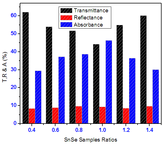 | Figure 9. Shows how averages of transmittance, reflectance and absorbance of SnSe thin films varied with ratios in visible region |
3.1.8. Optical Band Gap Energies for Tin Selenide (SnxSey) Thin Films
- A graph of (Eα)2 against energy drawn using data from Scout 98 programme was used to calculate the band gap energy. From the optical absorbance vs. wavelength data was obtained and using equation
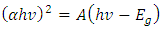 | (9) |
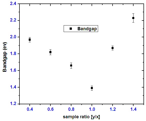 | Figure 10. SnSe thin films of forbidden energy band gap varying with ratios |
3.2. Nickel Doped Tin IV Oxide (SnO2: Ni)
3.2.1. Optical Transmittance Spectra for SnO2: Ni Thin Films
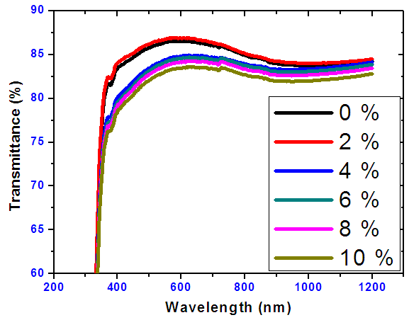
- Figure 11 shows the optical transmittance for nickel doped tin IV oxide at different doping percentages. The optical transmittance of SnO2 and Nickel doped SnO2 was found to be above 75% in the VIS and NIR region.
 | Figure 11. Graph of transmittance spectra of Tin oxide doped with thin Nickel Films |
3.2.2. Optical Reflectance Spectra for SnO2: Ni Thin Films
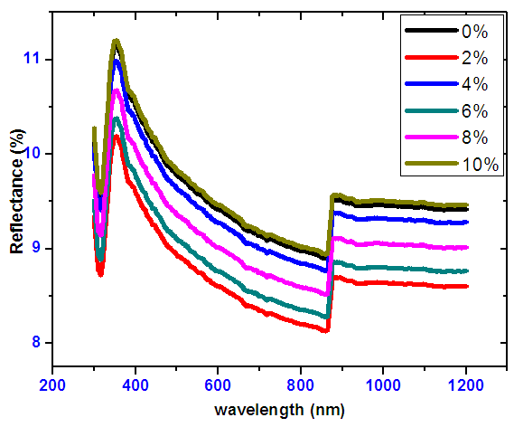
- The plots in Figure 12, displays a spectra of reflectance. Reflectance was low and lying in the range of 8-10% in the infra-red region, ultra violet and visible range of the solar spectrum. For both doped and undoped SnO2 the overall reflectance is fairly low. At around 850 nm a kink is observed, this is caused during the exchange of hydrogen lamp and Deuterium lamp.
 | Figure 12. Optical reflectance spectra for Nickel doped Tin oxide |
3.2.3. Refractive Index for Nickel Doped Tin Oxide
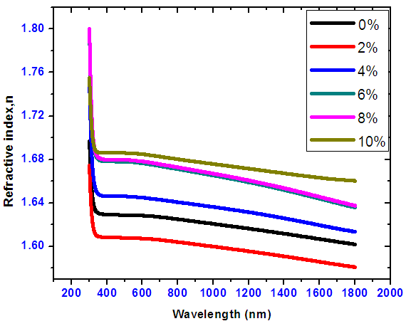
- Refractive indices decreased against wavelength from 280-325 nm as shown in Figure 13. There were no meaningful vicissitudes of refractive indices as wavelength increased from 325-800 nm for undoped and doped Tin oxide. 2% Nickel doped tin IV oxide recorded the least refractive index. This means the photons travels through the film faster hence absorption is minimal.
 | Figure 13. Refractive index versus wavelength for Nickel doped Tin oxide |
3.2.4. Absorption Coefficient for Nickel Doped Tin IV oxide
- Figure 14 shows absorption coefficient for SnO2: Ni samples. The SnO2: Ni has a low absorption coefficient at high wavelengths and a high absorption coefficient at low wavelengths. Absorption of illuminated photon is higher at lower wavelengths hence high absorption coefficient as seen in the figure. This occurs because at lower wavelength, photons have high energy compared to the band gap and therefore very well absorbed. There was an observed lowest average absorption for films with 2% Nickel doping concentration within the visible range. At high wavelengths we observe very low absorption. This is because at high wavelengths, the photons have low energy hence mainly transmitted since band gap energy is not exceeded.
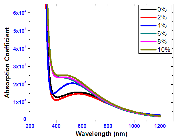 | Figure 14. Absorption coefficient versus wavelength for Nickel doped Tin IV oxide |
3.2.5. Extinction Coefficient for Nickel Doped Tin IV oxide
- Figure 15 shows the extinction coefficient versus wavelength. The average extinction coefficient within the visible range was below 0.2. The extinction coefficient is to a great extent increased at low wavelengths (< 350nm). This indicates that at low wavelengths, the films have high absorption. The extinction coefficient is also decreased at higher wavelength (> 750nm), this implies that the material became almost transparent at higher wavelengths. A film of 2% has the lowest extinction coefficient in the visible region.
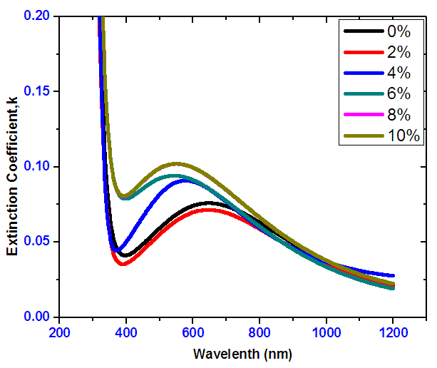 | Figure 15. Extinction coefficient versus wavelength for Nickel doped Tin IV Oxide |
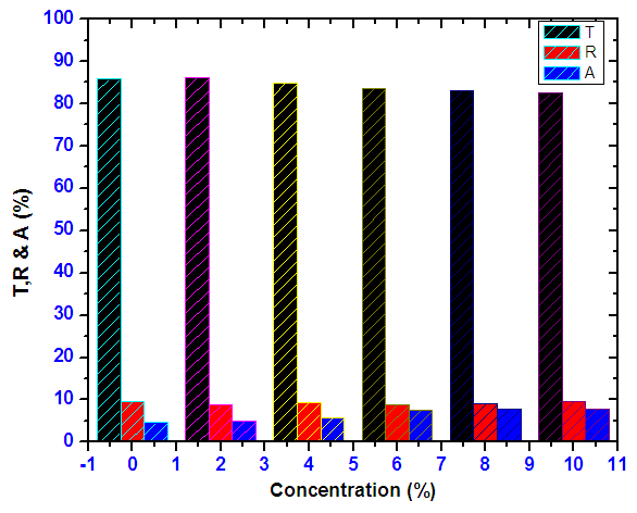
3.2.6. Averages of Transmittance, Absorbance and Reflectance in Visible Region for Nickel Doped Tin IV Oxide
- Figure 16 shows how averages of transmittance, reflectance and absorbance of Nickel doped Tin oxide thin films varied with Nickel concentration in visible region. It is clearly seen a sample of 2% Nickel has the highest Transmittance. The average transmittance in VIS region is above 80% whereas reflectance and absorbance are below 10% for the samples. This is in close range with the 1.5% Ni doped SnO2 optimized by [4]. Therefore 2% Nickel doped SnO2 shows properties of a good window layer for photovoltaic applications.
 | Figure 16. Shows how averages of transmittance, reflectance and absorbance of Nickel doped Tin IV oxide thin films varied with ratios in visible region |
3.2.7. Optical Band Gap Energies for Nickel Doped Tin IV Oxide
- The band gap energy values for Nickel doped Tin IV oxide were calculated by the scout 98 program. Using the mathematical treatment of the data the transition type and the band-gap energy can be derived from the optical absorbance against wavelength using equation 9. Since Nickel doped Tin IV oxide is a direct allowed band gap. Figure 17 shows how to obtain the band gap using Tauc relation. When a linear graph is drawn the band gap of the sample is obtained at a point where the line cuts the energy axis.
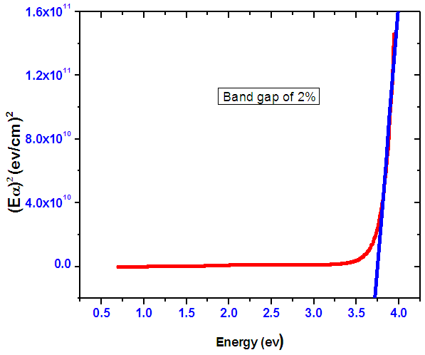 | Figure 17. A graph showing how to obtain the band gap for Nickel doped Tin oxide using Tauc relation equation 9 |
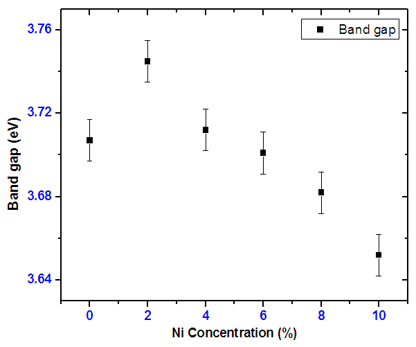 | Figure 18. Graph of band gap energy with varying doping concentration |
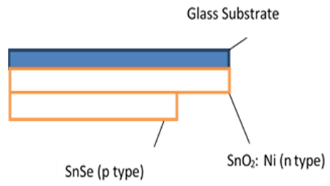
3.3. Fabrication and Characterization of SnSe-SnO2: Ni p-n Junction
- Fabrication of the p-n junction solar cell with glass/SnO2: Ni/SnSe/Al was achieved in stages. The SnO2: Ni film which acts as a window layer, in this case n type layer was coated onto a microscope glass substrate and an absorber thin film of SnSe coated onto SnO2: Ni on the same substrate to make a p-type layer. Fabrication was completed by deposition of Aluminium as rare contact on SnSe film to complete the solar cell as shown on figure 19.
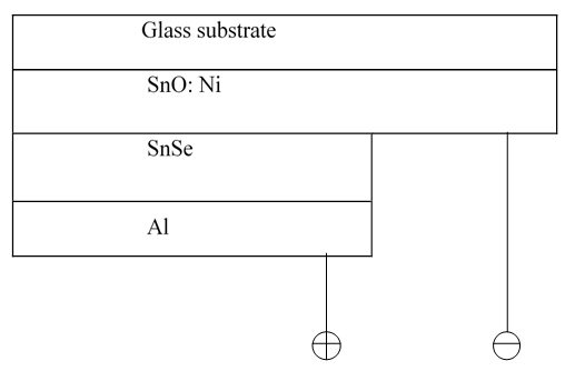 | Figure 19. Fabricated SnO2: Ni/SnSe/Al p-n junction solar cell schematic diagram |
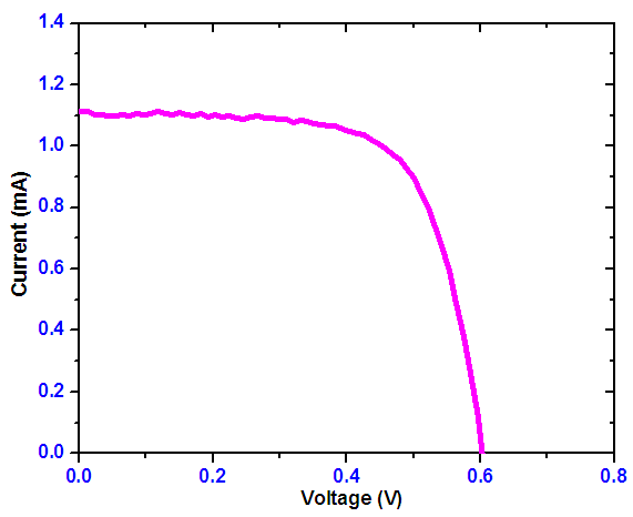 | Figure 20. Simulated I-V characteristic of the fabricated SnSe-SnO2: Ni p-n solar cell |
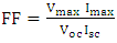 | (10) |
 | (11) |
4. Conclusions
- The efficiency of 0.4609% was quite low in comparison to Beyond 11% efficiency: Characterization of state of the art Cu2ZnSn(S,Se)4 solar cells. Recent performance enhancement in Cu2ZnSn(S1-xSex)(CZTSSe) devices, in which indium and gallium from CIGSSe are replaced by a more abundant and lower cost Zinc and tin have efficiencies of over 11%. Evidence has shown moderate thickness of the absorber layer CZTSSe (about 200 nm thickness) and a band gaps in the range 1.08 – 1.12 eV. A Ni-AL collection grid and ~ 110 nm thick MgF2 antireflection coating were deposited. Scanning electron Microscopy (SEM) was conducted. Scanning transmission electron microscopy (STEM) images were taken [26].CZTSSe (Kesterite – type crystal structure) was reported in 1996 to have an efficiency of 0.66%. Subsequent optimization using both evaporation and sputtering led to performance of 6.7% in 2008. Hydrazine – based deposition process was announced with efficiency of 9.7% which further improved to 10.1% in 2011. The highest certified power conversion efficiency at the 11.1% level was reported in 2012 [26]. Further studies on SnO2: Ni/SnSe and modern performance enhancement can lead to improvement of this efficiency.
ACKNOWLEDGEMENTS
- The authors would like to thank University of Nairobi, Kenyatta University and Chuka University Physics Departments for their support.