American Journal of Materials Science

p-ISSN: 2162-9382    e-ISSN: 2162-8424

2017;  7(2): 25-34

doi:10.5923/j.materials.20170702.01


Structural, Dielectric and Impedance Studies of KNNS–BKT Ceramics

Madan Lal 1, M. Chandrasekhar 2, Radheshyam Rai 1, Pawan Kumar 2

1School of Physics and Materials Science, Shoolini University (H.P) India 173229

2Department of Physics and Astronomy, National Institute of Technology, Rourkela, 769008 Odisha, India

Correspondence to: Radheshyam Rai , School of Physics and Materials Science, Shoolini University (H.P) India 173229.

Email:

Copyright © 2017 Scientific & Academic Publishing. All Rights Reserved.

This work is licensed under the Creative Commons Attribution International License (CC BY).
http://creativecommons.org/licenses/by/4.0/

Abstract

Polycrystalline (K0.4Na0.6Nb0.96Sb0.04)1-x-(Bi0.5K0.5TiO3)x (abbreviated as KNNS–BKT) ceramics have been prepared by the solid-state reaction method. Preliminary X-ray diffraction structural study showed the formation of polycrystalline sample with ABO3 type of perovskite structure and monoclinic symmetry of the ceramics. KNNS-BKT with x = 0.01 ceramics showed an optimum properties (ε ~ 3079, tan δ ~ 0.652, Tc ~ 230°C). Dielectric and impedance properties of x = 0.01 ceramics have been characterized at different temperature (RT to 400°C) and in 1kHz to 1MHz frequency range. The complex impedance plot exhibited one impedance semicircle, observed at low temperature, whereas two semicircles were observed above 150°C and the centres of the semicircles lie below the real axis, which indicates that the material is non-Debye type. Single impedance semicircle was related to the bulk grain effect and double semicircles were related to bulk and grain boundary effects. Bulk resistance and grain boundary resistance decreased with the increase of temperature, which confirmed negative temperature coefficient of resistance behaviour (NTCR).

Keywords: Oxide materials, Solid State Reaction method, Crystal structure, X-ray diffraction, Impedance spectroscopy

Cite this paper: Madan Lal , M. Chandrasekhar , Radheshyam Rai , Pawan Kumar , Structural, Dielectric and Impedance Studies of KNNS–BKT Ceramics, American Journal of Materials Science, Vol. 7 No. 2, 2017, pp. 25-34. doi: 10.5923/j.materials.20170702.01.

1. Introduction

Pb based ceramics have ruled the industries in the field of piezoelectric actuators, sensors, and transducers owing to their excellent piezoelectric properties [1, 2]. However, the Pb containing raw materials are toxic in nature and cause serious harm to human health as well as to environment with respect to pollution [3]. Therefore, there is a need to develop lead-free ceramics having high piezoelectric responses as those of lead-based ones possess significant economic and social values [4-7]. Bi0.5Na0.5TiO3 (BNT), K0.5Na0.5NbO3 (KNN), Bi0.5K0.5TiO3 (BKT) are well known lead free ferroelectric materials with perovskite structures that have been investigated during the last years [8]. K0.5Na0.5NbO3 lead-free piezoelectric ceramics have attracted much attention as one of the most possible substitution of lead-based ceramics in the last few years for their good piezoelectric and electromechanical properties [9-13]. Another reason is that KNN under goes several phase transitions with increasing temperature: rhombohedral to orthorhombic (R–O) transition at 123°C, orthorhombic to tetragonal (O–T) transition at 200°C, and tetragonal to cubic (T–C) transition at 410°C, respectively [14, 15]. However, pure KNN ceramics are difficult to densify by an ordinary sintering technique due to the evaporation of the alkali elements at high temperatures. Thus doping or modification of chemical composition have been tried to improve sinterability and consequently piezo-electric properties of KNN ceramics [16-18]. Recent finds show that perovskite structure doping can be an effective way of improving the electrical properties of KNN ceramics [19-21]. Nowadays, ion substitution becomes one of the most effective ways to enhance piezoelectric properties of KNN ceramics, such as Bi+3, Ta+5, Sb+5, Zr+4, and so on [22-25]. In 2004, Saito et al. reported that the Li+, Ta+5, Sb+5 -modified KNN textured ceramics exhibited excellent piezoelectric properties (d33 ~ 416 pC/N and kp 0.61), which can be comparable with soft lead zirconate titanate (PZT)-based ones [6]. In recent years many researcher have been reported KNN based composites with secondary system like K0.5Na0.5NbO3- Bi0.5K0.5TiO3 (KNN-BKT) [8], K0.5Na0.5Nb0.94O3-LiTaO3 (KNN-LT) [26], (K0.48Na0.52)(Mo2/3Bi1/3)(Nb0.97Sb0.03O3)-(Bi0.5Na0.5ZrO3) (KNMBNS–BNZ) [16], (K0.49Na0.51)(Nb0.95Sb0.05)O3– Bi0.5(Na0.82K0.18)0.5ZrO3 (KNNS–BNKZ) [4], K0.5Na0.5NbO3–LiSbO3 (KNN-LS) [27], (Na0.52K0.48) (Nb0.94Sb0.06)O3–LiTaO3 (KNNS-LT) [28], K0.4725Na0.4725Li0.055NbO3–AgSbO3 (KNNL-AS) [29] etc.
In this report, we are presenting the structural properties and impedance study of KNNS-BKT system namely (K0.4Na0.6Nb0.96Sb0.04)1-x-(Bi0.5K0.5TiO3)x (where x = 0.01, 0.03, 0.05, 0.07). In this series KNNS-BKT with x = 0.01 reveals the best results. The ceramic (K0.396Na0.5946Nb0.9504Sb0.0396)-(Bi0.005K0.005Ti0.01O3) have 260 nm average crystallite size. The electrical behavior showed that the ceramic haves Curie temperature at 230°C. The ceramics have dielectric constant (ε = 3079) and dielectric loss (tan δ = 0.652) at Curie temperature (i.e. 230°C) for 1kHz frequency. The bulk resistance and grain boundary resistance of the materials decrease with the increasing temperature, showing negative temperature and a typical semiconducting property, i.e. negative temperature coefficient of resistance behaviour.

2. Materials and Method

Polycrystalline samples of (K0.4Na0.6Nb0.96Sb0.04)1-x- (Bi0.5K0.5TiO3)x ceramics were synthesized from high purity oxides K2CO3 (99.99%), Na2CO3 (99%), Nb2O5 (99.9%), TiO2 (99.99%), Sb2O3 (99.99%), Bi2CO3 (99.9 wt.%), by using a solid state reaction technique (in which x = 0.01, 0.03, 0.05, and 0.07). For each composition, the raw materials were weighed according to the stoichiometric formula and milled in ethanol media for 12hrs, using agate mortar and pestle. After which the samples were dried at 100°C. Then the samples were calcined at temperatures at 900°C for 4 hrs. The samples were grinded thoroughly to ensure that there were no agglomeration in powder. The fine powder was cold pressed into cylindrical pellets of 10 mm in diameter and 1–2 mm in thickness using a hydraulic press with a pressure of 60 MPa. These pellets were sintered at a temperature 1000°C for 3 h. The formation and quality of compounds were verified with X-ray diffraction (XRD) technique. The XRD patterns of the compounds were recorded at room temperature using X-ray powder diffractometer with Cu Ka radiation (k = 1.5405 Å) in a wide range of Bragg angles 2h (20°≤ 2θ ≤ 60°) at a scanning rate of 2 deg min-1. The flat polished surfaces of the sintered samples were electrode with air drying silver paste. Impedance were determined by use of HIOKI IM3570 Impedance Analyzer at frequencies 1 kHz–1 MHz; samples were heated from room temperature to 400°C.

3. Results and Discussion

Figure. 1 shows the XRD patterns at room temperature for (K0.4Na0.6Nb0.96Sb0.04)1-x-(Bi0.5K0.5TiO3)x (Where x = 0.01, 0.03, 0.05, 0.07 ) prepared by solid state reaction method. It was found that these compositions exhibit perovskite structure with monoclinic structure. In compositions with x = 0.03, 0.05 and 0.07 where a small amount of secondary phase shown as * (i.e. Na3SbO3, ICDD: 44-0934) is detectable. The xrd peaks relative intensities obtained for the KNN meets with the JCPDS file no. 770038 and conform that structure is monoclinic at room temperature. All the reflection peaks were indexed using observed inter-planar spacing d, and lattice parameters of sample was determined by using the least-squares refinement method. The calculated and observed d values of all diffraction lines (reflections) of the K0.396Na0.5946Nb0.9504Sb0.0396-Bi0.005K0.005Ti0.01O3 ceramic is given in Table 1.
Figure 1. X-ray diffractometer patterns of (K0.4Na0.6Nb0.96Sb0.04)1-x-(Bi0.5K0.5TiO3)x (where x = 0.01, 0.03, 0.05 and 0.07) ceramics
Table 1. Comparison of Lattice parameters of K0.396Na0.5946Nb0.9504Sb0.0396Bi0.005K0.005Ti0.01O3 ceramic
     
Figure. 2(a) shows the fitting of XRD peaks for (002), (220) and (004) planes of K0.396Na0.5946Nb0.9504Sb0.0396Bi0.005K0.005Ti0.01O3 ceramic fitted to the Gauss function. The coefficient of determination of fitted peaks to Gauss function is closer to unity compared to the other functions. This coefficient is symbolized by R2, which is interpreted as the goodness of fit of a regression. An R2 close to unity indicates that a regression line fits the data well, whereas an R2 closer to zero indicates a poor fitting of peak. The FWHM values of the peaks (FWHMobs) measured from the fitted peaks are given in Table 2.
Figure 2. (a) Shows the XRD peaks from 002, 220 and 004 planes fitted to the Gaussian function and (b) variations of FWHMtot.cosθ with sinθ of K0.396Na0.5946Nb0.9504Sb0.0396Bi0.005 K0.005Ti0.01O3 ceramic
Table 2. Details of the parameters used to calculate the strain of K0.396Na0.5946Nb0.9504Sb0.0396Bi0.005 K0.005Ti0.01O3 ceramic
     
Stripping the instrumental, strain and size broadening factors depends on the shape of the peaks. For Gauss peaks, the relation is defined as follows:
(1)
Where FWHMsize is the peak broadening due to the fine grain size, FWHMstrain is the peak broadening due to the lattice strain and FWHMinst: is the peak broadening due to the instrumental effects. Estimation of the instrumental broadening (FWHMinst) is desirable to correct the width of different peaks. FWHMinst: is determined by fitting the XRD profiles to a Gauss function given in Table 2. FWHMtot involving both FWHMsize and FWHMstrain can be expressed as
(2)
Rewrite equation for lattice strain and particle size effects:
(3)
Where
(4)
D = grain diameter, k = 0.9 to 1.0 depending upon grain shape and Cε0 = Strain in the material.
On solving equation (3)
(5)
(6)
Comparing the (5) and (6), m = Cε0 = slope = strain of sample.
Figure 2(b) shows the variation of FWHMtot.cosθ with sinθ and the slope of this plot is used to calculate the strain of the material as explained in the above equation and the strain in our material is ~1.91%. All the reflection line in
XRD pattern were used for obtaining the average crystalline size using the Debye‑Scherrer equation [30].
(7)
where β = FWHMtot. Calculated using eqn. (3), D is the diameter of the particle, λ is the x-ray wavelength (0.154 nm),
FWHMobs and FWHMinst are the measured peak broadening and instrumental broadening in radian, respectively, and θ is the Bragg angle of the reflection. The calculated average crystalline size from eqn. (7) is ~ 260 nm.

3.1. Dielectric Studies

Figure 3 shows the variation of dielectric constant (ε) as a function of temperature of K0.396Na0.5946Nb0.9504Sb0.0396Bi0.005 K0.005Ti0.01O3 ceramic at frequency 1 kHz. As in normal ferr-oelectrics, the dielectric constant of K0.396Na0.5946Nb0.9504Sb0.0396Bi0.005K0.005Ti0.01O3 ceramic increases gradually with the increasing temperature up to the transition temperature and thereafter it decreases smoothly with the increasing temperature. The maximum observed value of εmax = 3079 at Tc = 230°C corresponds to the ferroelectric paraelectric phase transition temperature. In Figure 3 shows that tan δ decreases sharply at with the increasing temperature above 50°C. The minimum observed value of tan δ = 0.028 at Tc = 230°C.
Figure 3. Variation of dielectric constant (ε) and dielectric loss (tanδ) for K0.396Na0.5946Nb0.9504Sb0.0396Bi0.005 K0.005Ti0.01O3 ceramic at 1 kHz frequency
The degree of disorder of the sample was evaluated measure of diffuseness of the ferroelectric to paraelectric phase transition. The logarithmic plots related to this equation are shown in Figure 4. The values of γ is found to about 2.2. An alternative approach was also adopted to estimate the degree of diffuseness using the relation ln (1/ε-1/εmax) = (T-Tmax)2/2 δg2 in which δg is the Gaussian [31, 32]. From the value of δg, which is related to the broadening of ε (T) curve, we can determine the degree of compositional fluctuations in the material.
Figure 4. Variation of ln(1/ε-1/εmax) versus ln(T-Tmax) of K0.396Na0.5946Nb0.9504Sb0.0396Bi0.005K0.005Ti0.01O3 ceramic at 1 kHz frequency

3.2. Impedance Study

Complex Impedance spectroscopy (CIS) is a powerful tool to separate out the grain boundary and grain-electrode effects, which usually are the sites of trap for oxygen vacancies and other defects. It is also useful in establishing space charge polarization and its relaxation mechanism, by aptly assigning different values of resistance and capacitance to the grain and grain boundary effects. A remarkable aspect of the impedance analysis is the option of calculating the different contributions to the conductivity, namely the bulk, grain boundary and grain-electrode contributions.
Figure 5(a) shows the variation of the real part (Z′) of impedance as a function of log frequency (1kHz – 1MHz) at different temperatures. The Z′ increase slowly in the low frequency range depending on the temperature, and falls off sharply with an increase in frequency. The value of Z′ is larger in the low frequency range and gets a monotonous decrease with rise in frequency. It may be due to the effect of polarization in the sample. Interestingly, the magnitude of Z′ is found to decrease with the rise in temperature as shown in Figure 5(a) which suggests the typical negative temperature coefficient of resistance (NTCR) type behavior of ceramics material, usually observed in semiconductors [33, 34]. The higher values of Z′ at lower frequencies and higher temperatures indicate that the polarization in our material is larger. The temperature at which this frequency-dependent to frequency-independent change of Z′ occurs, varies with frequency in the material composition. This also signifies that the resistive grain boundaries become conducting at these temperatures and that the grain boundaries are not relaxing even at the highest measurement ranges of frequency and temperature. Figure 5(b) shows the variation of the imaginary part (Z″) of impedance as a function of frequency (f). Z″ (f) plot shows almost identical monotonically decreasing type of variation up to the same frequency limit ~10 kHz beyond which they merge together at a very low value of Z″ to show frequency-independent nature of variation extending up to the highest frequency limit at all the chosen measurement temperatures. The merger of Z″ (as well as of Z′) at higher frequencies for all the temperatures indicates possible release of space charge accumulation at the boundaries of homogeneous phases in our material under the applied external field. At lower temperatures, monotonic decrease of Z″ at lower temperatures the relaxation is absent in the material system. This means that relaxation species are immobile defects and the orientation effects may be associated. Also, the decreasing magnitudes of Z′ and Z″ with increasing frequencies implied that relaxation in the material is temperature-dependent, and that there is no single relaxation time. At 1 kHz frequency, the maximum and minimum values of Z′ are ~ 932 kΩ and ~98kΩ and of Z″ are ~ 11.42 kΩ and ~ 2049 kΩ for x=0.01 sample respectively.
Figure 5. (a) Variation of real part (Z′) and (b) imaginary part (Z″) of impedance with frequency at different temperatures of K0.396Na0.5946Nb0.9504Sb0.0396Bi0.005 K0.005Ti0.01O3 ceramic
Figure 6(a) shows the Cole-Cole plots of the compound from room temperature to 400°C. All the resulting curves showed a tendency to bend towards the abscissa to form semicircles with their centers below the real axis, having comparatively smaller radii. Further, the radii decrease with the increase of temperature, thereby indicating negative temperature coefficient of resistivity (NTCR) behaviour of the materials, generally found in case of semiconductors and at the same time showing a clear-cut departure from the ideal Debye type behaviour. This non-ideal behavior could be attributed to several factors such as grain orientation, grain boundary, stress-strain phenomena, and atomic defect distribution. Complex impedance spectrum is distinguished by semicircles. A series array of two parallel RC combinations [(Rg, Cg), (Rgb, Cgb)] in series with a resistor (Rs) indicate the contribution from grains of the sample in the high frequency region and from the grain boundaries in the low frequency region. No other relaxation mechanism, such as the electrode effects, could be identified through the use of CIS technique in the test frequency and temperature range. Further, it is not possible to get two clearly separated semicircles on the same impedance plot.
Figure 6(b) shows the fitting at 100°C 350°C, and 400°C of Nyquist plot, respectively. It is observed that with the increase in temperature the slope of the lines decreases and the lines bend towards real (Z′) axis. A semicircle of the graph indicates that the conductivity of the sample increases. It can also be observed that the peak maxima of the plots decrease and the frequency for the maximum shifts to higher values with the increase in temperature. It can be noticed that the complex impedance plots are not represented by full semicircle, rather the semicircular arcs are depressed and the centres of the arcs lies below the real (Z′) axis suggesting the relaxation to be of poly-dispersive non-Debye type in sample. This may be due to the presence of distributed elements in the material electrode system [35, 36]. An equivalent circuit is being used to provide a complete picture of the system and establish the structural property relationship of the materials. Comparison of complex impedance plots (symbols) with fitted data (lines) has been given in Figure 6(b). To model the non-Debye response, constant phase element is used in addition to resistors and capacitors.
Figure 6. (a) Variation of real and imaginary part of impedance at different temperatures of K0.396Na0.5946Nb0.9504Sb0.0396Bi0.005K0.005Ti0.01O3 ceramic and (b) Fitting of Cole–Cole plot of K0.396Na0.5946Nb0.9504Sb0.0396Bi0.005K0.005Ti0.01O3 ceramic for 100°C, 350°C and 400°C temperatures
Complex modulus analysis is an alternative approach to explore electrical properties of the material and magnify any other effects present in the sample (which are unidentifiable or overlapping in CIS technique) as a result of different relaxation time constants. It is an important and convenient tool to determine, analyze and interpret the dynamical aspects of electrical transport phenomena (i.e. parameters such as carrier/ion hopping rate, conductivity relaxation time, etc.). In order to analyze and interpret the experimental data, it is essential to have a model equivalent circuit that provides a realistic representation of the electrical properties. The modulus representation suppresses the unwanted effects of extrinsic relaxation often used in the analysis of dynamic conductivities of ionically conducting glasses. The dielectric modulus (M*=1/ ε*) is frequently used in the analysis of dielectric data of ionic conductors [37]. The advantage of adopting complex electrical modulus spectra is that it can discriminate against electrode polarization and grain boundary conduction processes. Using electric modulus analysis, it is easier to relate this phenomenon to other properties, especially the dynamical mechanical modulus and can be written as a single function of conductivity. Sinclair and West [33, 37] suggested the combined usage of impedance and modulus spectroscopic plots to rationalize the dielectric properties. Only one peak in Z″ (f) vs Z′ (f) plots but two peaks in M″ (f) vs M′ (f) plots at all the test temperatures for all the compositions taken for analysis in the present study suggest that the impedance data can be better analyzed by re-plotting them in the modulus formalism. The peak heights are proportional to R for the Z″ (f) vs Z′ (f) plots and to C−1 for the M″ (f) vs M′ (f) plots. Complex impedance plane plots of Z″ versus Z′ (where Z′ and Z″ are the real and imaginary parts of the complex impedance (Z*), respectively) are useful in determining the dominant resistance of a sample but are insensitive to the smaller values of resistances. Similarly, complex modulus plots are useful in determining the smallest capacitance. Thus, the power of combined usage of both impedance and modulus spectroscopy is that the Z′- Z″ plot highlights the phenomenon of largest resistance whereas M″ vs. M′ picks up those of the smallest capacitance [38]. The additional contribution in the low frequency part to the specific semicircle is attributed to the blocking effect of the pores. Also the poor separation of the overlapped semicircles is ascribed to the blocker (pore) size and if the blocker size is greater than 1μm, it would lead to the overlapping of the semicircles [39].
Figure 7 shows the complex modulus plots of x=0.01 samples corresponding to the several temperatures (i.e., room temperature to 400°C). From this figure, we can notice that the samples’ modulus spectrum has a typical semicircular pattern with its center lying below the real axis, thereby indicating non-Debye type of relaxation response in the investigated material system. In the modulus spectrum, there is formation of two semicircles in this set above 150°C up to 400°C. These semicircles indicate that both grain and grain boundary capacitance started playing active roles in the conduction mechanism of the material system at higher temperatures.
Figure 7. Variation of real and imaginary part of modulus at different temperatures of K0.396Na0.5946Nb0.9504Sb0.0396Bi0.005 K0.005Ti0.01O3 ceramic
Figure 8(a) and (b) shows the normalized plot of Z″/Z″max and M″/M″max versus log (f/fmax) at different temperatures for (K0.396N0.5946Nb0.9504Sb0.0396)-(Bi0.005 K0.005Ti0.01O3) material, respectively. The normalized plot overlaps on a single master curve at different temperatures as shown in Figure 8(a) and (b) (i.e. same shape and pattern in the peak position with slight variation in full width at half maximum (FWHM) with the rise in temperature). Thus, the dielectric processes occurring in the material can be investigated via the master modulus plot. The value of FWHM evaluated from the normalized spectrum is greater than log (2 + √3) /(2 - √3), and this indicates about the non-Debye-type behaviour which is well supported by the complex modulus plot.
Figure 8. (a) Scaling behavior of (Z″/Z″max) and (b) (M″/M″max) versus log (f/fmax) of K0.396Na0.5946Nb0.9504Sb0.0396Bi0.005K0.005 Ti0.01O3 ceramic at different temperature
Figure 9(a) shows the log-log plot of ac electrical conductivity (σac) versus frequency at different temperatures of x=0.01 samples. The electric conductivity in ceramics is mainly controlled by the migration of charge species under the action of electric field and by the defect-ion complexes, the polarization field, the relaxation etc. The σ (f) curves are found to be merging at high frequency and temperature regions, suggesting the less defect mobility and low conductivity in the material. The phenomenon of the conductivity dispersion in the materials is generally analyzed by using A.K. Jonscher’s law [40]
(8)
where σdc is the frequency independent conductivity which can be obtained by extrapolating the low frequency plateau to zero frequency, A is a constant depending on temperature and determines the strength of polarization and n is an exponent less than or equal to unity which represents the degree of interaction between mobile ions and its surrounding lattices [41]. The plots show that the real part of ac conductivity changes by about three to four orders of magnitude in the measurement ranges of frequency (from 1 kHz to 1 MHz) and temperature (from the temperature 30°C to 500°C). Figure 9(b) shows the plot of ln σac as a function of reciprocal temperature (103/T) at selected frequencies (i.e. 1 kHz, 10 kHz). It is observed from the plot that in the low temperature region, ac conductivity of the composition increased with increase in frequency, however a bit slowly, thereby indicating dispersion of conductivity with frequency. With increase in temperature, dispersion in conductivity narrowed down and all the curves for different frequencies appeared to merge at high temperatures, although they didn’t merge completely. The activation energy for conduction was obtained using the Arrhenius relationship
(9)
(10)
The slope of the linear least- squares- fit of the conductivity data to eqn. (10) gives the value of the apparent activation energy, Ea, KB is Boltzmann constant. The values of Ea for the sample at frequencies 1 and 10 kHz were found to be 1.18 and 0.87 eV respectively. As the temperature increases the ac conductivity also increases. This may be due to ionic solids having a limited number of mobile ions being trapped in relatively stable potential wells during their motion through the solid. Due to a rise in temperature the donor cations are taking a major part in the conduction process. The donors have created a level (i.e. band-donor level), which is much nearer to the conduction band. Therefore, only a small amount of energy is required to activate the donors.
Figure 9. (a) Variation of ac-conductivity with frequency at different temperature and (b) Variation of ac-conductivity with temperature at different frequencies of K0.396Na0.5946Nb0.9504Sb0.0396Bi0.005 K0.005Ti0.01O3 ceramic

4. Conclusions

Solid solutions of K0.396Na0.5946Nb0.9504Sb0.0396Bi0.005K0.005Ti0.01O3 ceramics have been prepared by solid-state reaction route. XRD patterns confirmed the monoclinic structure. Impedance spectroscopy confirmed the presence of bulk effect at low temperature and grain and grain boundary effects at more than 150°C temperature. Dielectric relaxation was found to be of non-Debye type and the dielectric relaxation frequency shifted to higher side with the increase in temperature. Nyquist plot and conductivity studies showed the NTCR behavior of the samples. These properties suggested the suitability of this system be used in sensor, actuator and transducer applications.

ACKNOWLEDGEMENTS

Authors are grateful to the Defence Research and Development Organization (DRDO), Govt. of India, for financial support under the research project ERIP/ER/1303129/M/01/1564.

References

[1]  B. Jaffe, and W.R. Cook Jr.. and H. Jaffe, “Piezoelectric Ceramics” Academic Press, New York, (1971).
[2]  T. Ibn-Mohammed, S. C. L. Koh, I. M. Reaney, A. Acquaye, D. Wang, S. Taylor and A. Genoves “Integrated hybrid life cycle assessment and supply chain environmental profile evaluations of lead-based (lead zirconate titanate) versus lead-free (potassium sodium niobate) piezoelectric ceramics” Energy & Environmental Science, (2016).
[3]  Ya-Ru Zhang, Jing-Feng Li , Bo-Ping Zhang, and Chun-E Peng “Piezoelectric and ferroelectric properties of Bi-compensated (Bi1/2Na1/2)TiO3–(Bi1/2K1/2)TiO3 lead-free piezoelectric ceramics” Journal of Applied Physics, (2008).
[4]  Yue-Ming Li, Zong-Yang Shen, Yi-Jun Liu, Wan-Cheng Shen and Zhu-Mei Wang “High piezoelectric response in KNNS–xBNKZ lead-free ceramics” Journal of Materials Science: Materials in Electronics, (2015).
[5]  Eric Cross “Materials science: Lead-free at last” Nature, (2004).
[6]  Yasuyoshi Saito, Hisaaki Takao, Toshihiko Tani, Tatsuhiko Nonoyama, Kazumasa Takatori, Takahiko Homma, Toshiatsu Nagaya, Masaya Nakamura “High performance lead-free piezoelectric material” Nature, (2004).
[7]  Kai Zhang, Yiping Guo , Di Pan, Huanan Duan, Yujie Chen, Hua Li, and Hezhou Liu “Phase transition and piezoelectric properties of dense (K0.48,Na0.52)0.95Li0.05SbxNb(1−x)O3-0.03Ca0.5(Bi0.5,Na0.5)0.5 ZrO3 lead free ceramics” Journal of Alloys and Compounds, (2016).
[8]  Amrita Singh and Ratnamala Chatterjee “Structural and electrical properties of BKT rich Bi0.5K0.5TiO3-K0.5Na0.5NbO3 system” AIP Advances, (2013).
[9]  Yongyong Zhuang, Zhuo Xu , Fei Li, Zhipeng Liao, and Weihua Liu “Fabrication of flexible energy harvesting device based on K0.5Na0.5NbO3 nanopowders” Journal of Alloys and Compounds, (2015).
[10]  Ting Zheng, Jiagang Wu, Dingquan Xiao, and Jianguo Zhu “Giant d 33 in nonstoichiometric (K, Na)NbO3-based lead-free ceramics” Scripta Materialia, (2015).
[11]  Zhiqiang Zhang, Jie Yang, Zhifu Liu, and Yongxiang Li “Evolution of textured microstructure of Li-doped (K,Na)NbO3 ceramics prepared by reactive templated grain growth” Journal of Alloys and Compounds, (2015).
[12]  Jialiang Zhang, Xing Tian, Yong Gao, Weizeng Yao, Yalin Qin, and Wenbin Su “Domain Structure of Poled (K0.50Na0.50)1−xLixNbO3 Ceramics with Different Stabilities” Journal of the American Ceramic Society, (2015).
[13]  Ying Lin, Jintao Zhang, Haibo Yang, and Tong Wang “Excellent piezoelectric and magnetoelectric properties of the (K0.45Na0.55)0.98Li0.02(Nb0.77Ta0.18Sb0.05)O3/Ni0.37Cu0.20Zn0.43 Fe1.92O3.88 laminated composites” Journal of Alloys and Compounds, (2017).
[14]  L. Egerton, and D.M. Dillon, “Piezoelectric and dielectric properties of ceramics in the system potassium—sodium niobate” Journal of the American Ceramic Society, (1959).
[15]  Tao Huang, Dingquan Xiao, Chao Liu, Fangxu Li, Bo Wu, Jiagang Wu, and Jianguo Zhu “Effect of SrZrO3 on phase structure and electrical properties of 0.974(K0.5Na0.5) NbO3–0.026Bi0.5K0.5TiO3 lead-free ceramics” Ceramics International, (2014).
[16]  Deqing Zhang, Feng Shi, Junye Cheng, Zhangjie Cheng, Xiuying Yang, Guangping Zheng, and Maosheng Cao “Modified hydrothermal synthesis and structural characterization of monoclinic (KxNa1− x)NbO3(0.05≤ x≤ 0.15) rods” Ceramics International, (2015).
[17]  Qiyi Yin, Zhaoqi Sun, Miao Zhang, Gang He, Yang Chen, Qing Wang, and Mingzhu Yan “Structure and electrical properties of K0.5Na0.5Nb0.94−xSb0.06SnxO3 lead-free piezoelectric ceramics” Journal of Alloys and Compounds, (2015).
[18]  Na Wei, Jin Wang, Bo Li, Yu Huan, and Longtu Li “Improvement of the piezoelectric and ferroelectric properties of (K, Na)0.5NbO3 ceramics via two-step calcination–milling route” Ceramics International, (2015).
[19]  Yunfei Chang, Zupei Yang, Lingling Wei, and Bing Liu “Effects of AETiO3 additions on phase structure, microstructure and electrical properties of (K0.5Na0.5)NbO3 ceramics” Materials Science and Engineering: A, (2006).
[20]  Xueyi Sun, Jun Chen, Ranbo Yu, Ce Sun, Guirong Liu, Xianran Xing, and Lijie Qiao “BiScO3 Doped (Na0.5K0.5)NbO3 Lead‐Free Piezoelectric Ceramics” Journal of the American Ceramic Society, (2009).
[21]  Fangyuan Zhu, T.A. Skidmore, A.J. Bell, T.P. Comyn, C.W. James, M. Ward, and S.J. Milne “Diffuse dielectric behaviour in Na0.5K0.5NbO3 – LiTaO3 – BiScO3 lead-free ceramics” Materials Chemistry and Physics, (2011).
[22]  Shujun Zhang, Jong Bong Lim, Hyeong Jae Lee, Ru Xia, and Thomas R. Shrout “(K0.5Na0.5)NbO3 based lead free piezoelectrics with expanded temperature usage range” 17th IEEE International Symposium on the Applications of Ferroelectrics, (2008).
[23]  Ruzhong Zuo, Xusheng Fang, Chun Ye, and Longtu Li “Phase Transitional Behavior and Piezoelectric Properties of Lead‐Free (Na0.5K0.5)NbO3–(Bi0.5K0.5)TiO3 Ceramics” Journal of the American Ceramic Society, (2007).
[24]  Masato Matsubara, Toshiaki Yamaguchi, Wataru Sakamoto, Koichi Kikuta, Toshinobu Yogo, and Shin-ichi Hirano “Processing and Piezoelectric Properties of Lead‐Free (K, Na)(Nb, Ta)O3 Ceramics” Journal of the American Ceramic Society, (2005).
[25]  Zhi Tan, Jianguo Zhu, Yuxing Zhang, Jie Xing, Qiang Chen, Bo Wu, Lingguang Sun, Jiagang Wu, Laiming Jiang, and Dingquan Xiao “Effects of Mo 2/3 Bi 1/3 doping on the phase structure, microstructure, and piezoelectric properties of KNNS–BNZ ceramics” Ceramics International, (2015).
[26]  Dai, Y., X. Zhang, and G. Zhou, “Phase transitional behavior in K0.5Na0.5NbO3–LiTaO3 ceramics” Applied Physics Letters, (2007).
[27]  Palei, P. and P. Kumar, “Dielectric, ferroelectric and piezoelectric properties of (1− x)[K0.5Na0.5NbO3] − x[LiSbO3] ceramics” Journal of Physics and Chemistry of Solids, (2012).
[28]  Jian Fu, Ruzhong Zuo, Xusheng Fang, and Kun Liu “Lead-free ceramics based on alkaline niobate tantalate antimonate with excellent dielectric and piezoelectric properties” Materials Research Bulletin, (2009).
[29]  Yuanyu Wang, Jiagang Wu, Dingquan Xiao, Jianguo Zhu, Ping Yu, Lang Wu, and Xiang Li “Piezoelectric properties of (Li, Ag, Sb) modified (K0.50Na0.50)NbO3 lead-free ceramics” Journal of Alloys and Compounds, (2008).
[30]  Sandeep Kumar, Neetu Ahlawat, and Navneet Ahlawat “Microwave sintering time optimization to boost structural and electrical properties in BaTiO3 ceramics” Journal of Integrated Science and Technology, (2016).
[31]  Alexei A. Bokov and Zuo-Guang Ye “Dielectric relaxation in relaxor ferroelectrics” Journal of Advanced dielectrics, (2012).
[32]  P. Kumari, R. Rai, A. L. Kholkin , and A. Tiwari “Study of Ca doping on A-site on the structural and physical properties of BLTMNZ ceramics” Advanced Materials. Letters, (2014).
[33]  D.C. Sinclair, and A.R. West, “Impedance and modulus spectroscopy of semiconducting BaTiO3 showing positive temperature coefficient of resistance” Journal of Applied Physics, (1989).
[34]  Karishma Kumari, Ashutosh Prasad, Kamal Prasad “Dielectric, Impedance/Modulus and Conductivity Studies on [Bi0.5(Na1-xKx)0.5]0.94Ba0.06TiO3(0.16≤x≤0.20) Lead-Free Ceramics” American Journal of Materials Science, (2016).
[35]  Seema Sharma, Kashif Shamim, Anand Ranjan, Radheshyam Rai, Poonam Kumari, and Sangeeta Sinha “Impedance and modulus spectroscopy characterization of lead free barium titanate ferroelectric ceramics” Ceramics International, (2015).
[36]  Shweta Thakur, Radheshyam Rai, Igor Bdikin, and Shashi Prakash Rai “Dielectric relaxation and ac conduction in multiferroic Bi0.8Gd0.1Pb0.1Fe0.9Ti0.1O3 ceramics: impedance spectroscopy analysis” Phase Transitions, (2016).
[37]  D.C. Sinclair, and A.R. West “Effect of atmosphere on the PTCR properties of BaTiO3 ceramics” Journal of materials science, (1994).
[38]  Li, H.-D., C.-D. Feng, and P.-H. Xiang “Electrical properties of La3+-doped (Na0.5Bi0.5)0.94Ba0.06TiO3 ceramics” Japanese journal of applied physics, (2003).
[39]  Ruzhong Zuo, Hongqiang Wang, Bing Ma, and Longtu Li “Effects of Nb5+ doping on sintering and electrical properties of lead-free (Bi0.5Na0.5)TiO3 ceramics” Journal of Materials Science: Materials in Electronics, (2009).
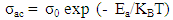
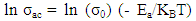
[40]  A.K. Jonscher “Dielectric relaxation in solids” Journal of Physics D: Applied Physics, (1999).
[41]  J.C. Dyre. and T.B. Schrøder “Universality of ac conduction in disordered solids” Reviews of Modern Physics, (2000).