-
Paper Information
- Next Paper
- Paper Submission
-
Journal Information
- About This Journal
- Editorial Board
- Current Issue
- Archive
- Author Guidelines
- Contact Us
American Journal of Materials Science
p-ISSN: 2162-9382 e-ISSN: 2162-8424
2016; 6(1): 1-18
doi:10.5923/j.materials.20160601.01

Dielectric, Impedance/Modulus and Conductivity Studies on [Bi0.5(Na1-xKx)0.5]0.94Ba0.06TiO3, (0.16 ≤ x ≤0.20) Lead-Free Ceramics
 Abstract
 Reference
 Full-Text PDF
 Full-text HTML
Karishma Kumari 1, Ashutosh Prasad 1, Kamal Prasad 2
1University Department of Physics, T.M. Bhagalpur University, Bhagalpur, India
2Centre for Nano-science and Nanotechnology, Aryabhatta Knowledge University, Patna, India
Correspondence to: Ashutosh Prasad , University Department of Physics, T.M. Bhagalpur University, Bhagalpur, India.
| Email: |  |
Copyright © 2016 Scientific & Academic Publishing. All Rights Reserved.
This work is licensed under the Creative Commons Attribution International License (CC BY).
http://creativecommons.org/licenses/by/4.0/

The present work encompasses the structural, microstructural, dielectric, impedance/modulus and conductivity studies on [Bi0.5(Na1-xKx)0.5]0.94Ba0.06TiO3, (0.16≤ x≤0.20) lead-free ceramics synthesized by conventional ceramic sintering technique in the frequency range 100 Hz-1MHz from the temperature of ambience up to 500°C. Effects of amount of K+ incorporation on the electrical properties and crystal structure were examined. X-ray diffraction analysis on the calcined powder samples shows that incorporated K+ diffuses into the lattice of morphotropic phase boundary composition [Bi0.5Na0.5]0.94Ba0.06TiO3 (BNBT6) to form a solid solution having the crystal structure with tetragonal symmetry. Complex impedance and modulus Cole–Cole plots showed the relaxation behaviour in the test materials to be of non-Debye type. Plots indicated grain and grain boundary contributions towards conductivity along with polarization and conductivity relaxation behaviour in the test complex ceramics. AC conductivity based activation energies have also been evaluated for the test ceramics.
Keywords: Solid state reaction, Grain boundaries, Dielectric properties, Impedance, Electrical conductivity, Actuators
Cite this paper: Karishma Kumari , Ashutosh Prasad , Kamal Prasad , Dielectric, Impedance/Modulus and Conductivity Studies on [Bi0.5(Na1-xKx)0.5]0.94Ba0.06TiO3, (0.16 ≤ x ≤0.20) Lead-Free Ceramics, American Journal of Materials Science, Vol. 6 No. 1, 2016, pp. 1-18. doi: 10.5923/j.materials.20160601.01.
Article Outline
1. Introduction
- In view of the grave concern and hence enforcement of regulations by European nations on the restrictions for the use of hazardous and eco-unfriendly lead-based materials in electrical and electronic devices, there is every possibility of complete ban on the use of such materials in near future. Consequently, lead-free materials, and especially ceramics, have attracted considerable global attention from researchers to find viable alternative candidates for device materials having comparable electrical and electromechanical properties such as for highly used lead zirconate titanate (PZT). In order to meet this vital requirement, several single, binary, and ternary compositions and their combinations have been tried by several researchers [1-27]. Out of these, the bismuth-based compounds were seen to be one of the good choices. First of all, bismuth sodium titanate (BNT) was considered, but in contrast with PZT, which has morphotropic phase boundary (MPB) composition at which it showed enhanced ferroelectric and piezoelectric properties, BNT is devoid of any such MPB. Additional deficient properties of BNT are high electrical conductivity (which hindered the ease in poling of the material), low remnant polarization (Pr), and high coercive field (Ec). The two temperature dependent anomalies in dielectric properties of the material, one at the depolarization temperature (Td) on the lower temperature side (that corresponds to the transition from the ferroelectric to the antiferroelectric phase) and the other at the Curie temperature (Tc) (that corresponds to the transition from the antiferroelectric to the paraelectric phase) on the higher temperature side, as well as the diffuse phase transition (DPT) showed BNT ceramics to be less useful for electronic and electromechanical device applications [5]. In an attempt at alleviating or removing the utmost possible deficient properties of BNT ceramics, binary solid solutions like BNT-BT [9-15] and BNT-BKT [16-21] were tried by several researchers as alternative useful lead-free piezoelectric materials for devices in view of the fact that each of these compositions was found to have an MPB. As regards the first composition i.e., BNT-BT, majority of research works reported so far have assumed the MPB between two phases-rhombohedral (BNT-rich) and tetragonal (BT-rich) at about 6-8mol% of BT. However, some recent Studies have shown the BNT unit cell to have monoclinic structure rather than rhombohedral. In order to remove the controversies in the different findings, the present research group carried out a systematic study on the structural and electrical properties of BNT-BT compositions for different amounts of BT ranging between 0.2-1.0 mol%. On the basis of the study, it was confirmed that the MPB lied at 6 mol% of BT (the composition hereinafter indicated as BNBT6) [21]. However, X-ray diffraction analyses used in the study revealed the MPB to be between monoclinic - tetragonal instead of between rhombohedral-tetragonal, as reported in majority of the previous works. The most recent study [28] has endorsed the findings of the present group on the basis of high resolution synchrotron X-ray powder diffraction data. The MPB for the second binary composition i.e., BNT-BKT, has been reported to be in the range 16-20 mol% of BKT [18, 19, 29]. It would not be inopportune to mention here that the MPB in a binary system is constrained in a very narrow composition range. In the aforementioned works, it has been suggested that in the ternary systems the MPB region may be extended to a wider compositional range. The combination of the above referred two binary compositions, (BNT-BT) and (BNT-BKT), in the form of ternary system BNT-BKT-BT has been studied systematically in the recent past and has been suggested to be good enough to replace PZT in certain applications such as ultrasonic wire bonding transducers and accelerometers [26]. As referred to earlier, the present group of workers conclusively derived that [Bi0.5Na0.5]0.94Ba0.06TiO3 (BNBT6) is the MPB composition between monoclinic and tetragonal phases. The proposed composition [Bi0.5(Na1-xKx)0.5]0.94 Ba0.06TiO3(hereinafter abbreviated as BNKxBT6) is nothing but a modified version of the BNT-BKT-BT ternary composition in which we are at liberty at varying only the K+ content (keeping the other constituents at our fixed optimized levels) instead of choosing the ratios of BNT, BKT, and BT by trial and error, as done by earlier researchers. This type of modified ternary composition is expected to yield the specific value of x for which the composite ceramic material gives the optimum dielectric, ferroelectric, and piezoelectric properties. Such a study of dielectric, ferroelectric, and piezoelectric properties along with complex impedance/modulus analyses on the said composition is reported for the first time with a view to examine whether this composition has the potentials of being a useful lead-free material candidate in electrical, electronic or electromechanical devices having properties comparable to its lead-based counterpart.
2. Materials and Methods
- The BNBT6 complex ceramics were first fabricated by conventional ceramics method via starting materials with metal oxide Bi2O3, BaCo3, TiO2, and the alkali carbonate powder Na2CO3(Hi-Media) (having a purity of more than 99.5% for each of them) in proper stoichiometric proportions as per the chemical formula of the composite. After that, four powder compositions of [Bi0.5(Na1-xKx)0.5] TiO3 with x = 0.16, 0.18, and 0.20 were prepared. These ingredient mixtures were separately mixed with BNBT6 samples to form the four test powder solutions. These dried powder samples were then mixed thoroughly for 2h using agate mortar and pestle, first in dry and then in wet methanol medium, for further 2h. The glue mixtures were allowed to dry in open air at least for two days and then were calcined at an optimized temperature of ~1080°C for 3h. After allowing the calcined powder test samples to cool slowly, by adding a small amount of polyvinyl alcohol (PVA) as a binder to the calcined powder, circular and rectangular disk shaped pellets for different compositions were fabricated having thicknesses~1-1.2mm and diameter ~10mm by applying uniaxial pressure ~ 125MPa using a hydraulic press. These pelletized samples were sintered at ~1090°C for ~2h in air atmosphere to achieve maximum density (~95% of the theoretical density). In order to avoid the loss of Na, K, and Bi, which is considerable at temperatures over 1000°C, most of the sintering processes were carried out with the with the green pelletized samples placed in alumina crucibles covered under BNKx BT6 powder. After the end of cooling process, the pellets were finely polished and electroded on both the opposite faces using a high grade (Ted Pele, USA) silver paste. The crystal structure of the samples was determined by XRD spectra observed on calcined powders of BNKx BT6 with an X-ray diffractometer (X’Pert-Pro, Pan Analytical, USA) at the temperature of ambience, using CuKα radiation (λ = 1.5405Å) over a wide range of Bragg angles (20°≤2θ≤80°). The microstructure was examined at the temperature of ambience over freshly fractured surfaces of the sintered pelletized samples using a scanning electron microscope (JEOL-JSM840A). The temperature-dependent dielectric constant (ε′), loss tangent (tanδ), and complex impedance were evaluated at various frequencies like 100Hz, 1kHz, 10kHz, 100kHz and 1MHz using the capacitance, impedance, and phase data obtained from a computer-controlled LCR Hi-Tester (HIOKI 3532-50, Japan) on a symmetrical cell of type AgceramicAg, where Ag is a conductive paint coated on either side of the pellet. These (d33) of the poled ceramic samples were measured by using a piezometer PM 3500 (KCF Technologies, USA). The P-E hysteresis loop at room temperature was traced using an automatic PE-loop tracer (Marine India Electrocom Ltd., New Delhi, India).
3. Results and Discussion
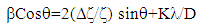
- Fig. 1 shows the XRD spectra of calcined BNKxBT6 powder. A standard computer program “POWD” was utilized for the XRD-profile analysis. Good agreement between the observed and calculated inter-planar spacing without any trace of secondary peaks (representatives of the constituent oxides) was found, thereby suggesting the formation of a single-phase compound. All the reflection peaks of the XRD pattern of the samples were indexed, and the lattice parameters were determined in the monoclinic as well as in tetragonal system of crystals. The presence of tetragonal as well as monoclinic phase in the compositions, possibly due to its constituents (BT, BKT) and BNT, respectively, is endorsed by the splitting of peaks between 44.5°-47.5° into two peaks (200) and (002) in the XRD patterns, as shown in Figure 1. This splitting becomes increasingly prominent with the further addition of K+. The most prominent peaks for each the samples is located at approximately 2θ = 31.86°, having hkl value (220).With increasing K+ content, the diffraction peaks are seen to shift to lower 2θ angles, thereby indicating an increase in the unit cell size. The magnitudes of the shifts were seen to increase in proportion to the concentration of K+ in the sample. This result is in accordance with the expectations, because the ionic radius of K+ (1.38 Å) is larger than that of Bi3+ (1.17 Å) as well as of Na+ (1.18 Å), which considerably distorts the lattice and hence lattice parameters are changed. An extended view of the XRD pattern shown in Fig. 1(b) and insert suggests that the MPB region consists of coexisting monoclinic and tetragonal phases over the entire compositional range. The composition BNKxBT6 is likely to be a mixture of monoclinic and tetragonal phases, but with a higher volume fraction of tetragonal phase over monoclinic phase. This is clearly seen by a noticeable splitting of (002)/ (200) peaks at 2θ ~ 46.5-47.5°. With an increase in the K+ mole content, the splitting in the (002)/ (200) peaks decreases and the peak shape becomes nearly symmetric for compositions near x = 0.20. The composition dependent trend in the splitting in the (002)/(200) peaks is more complex as shown in Fig. 1b.
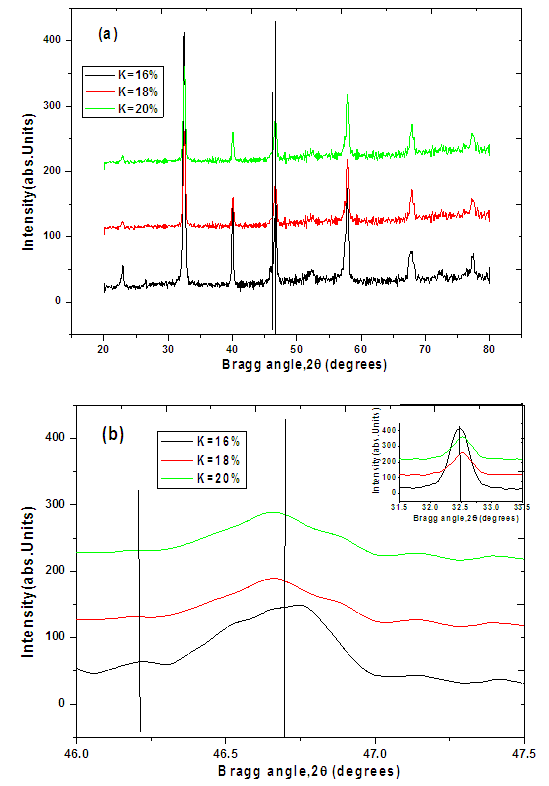 | Figure 1. (a) X-ray diffraction patterns of BNKxBT6 (x=0.16, 0.18, 0.20) ceramics sintered at 1190°C for 2 h in the range 2θ = 20 - 80°, (b) extended plot between 2θ = 46.0-47.5°, Insert: plot between 2θ = 31.5-33.5° |
 | (1) |
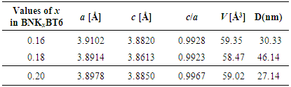
 was applied to estimate the diffraction width at half peak intensity. Here A and θc are the area and centre of the curve, respectively. Table 1 shows the variation of c/a ratio as a function of x. It may be noted that the c/a ratio and volume of the unit cell slightly decrease with increase of x up to x = 0.18 and then start increasing with higher substitution of Na+ ions by K+ ions. Apparent particle size as derived from Williamson-Hall plots first increasing trend from 33.33nm to 46.14nm up to x=0.18 and then diminishes to 27.14nm for x=0.20.
|
3.1. Microstructural Study
- Figure 2 shows the SEM micrograph of BNKxBT6 ceramic samples on 2-5 μm scale. The average grain size of all the three compositions was found to be~ 1 μm. The ratio of average crystallite size to the grain size of all the test ceramic samples is found to be of the order of 10-3. Further, the microstructures of all compositions were seen to consist of randomly oriented, non-uniform grains in shape and size and a certain amount of intergranular pores. Such behaviour of the grain growth reflects the competition between the driving force for grain boundary movement and the retarding force exerted by pores.
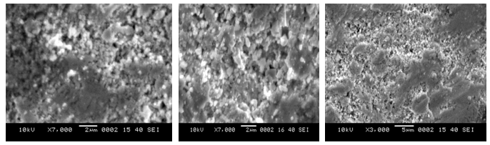 | Figure 2. SEM micrographs of BNKxBT6 ( x = 0.16,0.18,0.20) ceramics |
3.2. Dielectric Studies
- The frequency dependence of the dielectric constant (εr) and loss tangent (tanδ) at different temperatures has been plotted and shown in Fig. 3 & 4, respectively. It is observed that ε follows an inverse dependence on frequency, normally followed by almost all dielectric and/or ferroelectric materials. Dispersion with relatively high dielectric constant can be seen in the ε-f graph in the lower frequency region and dielectric constant drops at higher frequencies. The modified Debye equation related to a free dipole oscillating in an alternating field is expressed as:
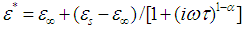 where εs and ε∞ are the low- and high-frequency value of ε, ω (=2πf) is the cyclic frequency - f being the frequency of measurement, τ the relaxation time and α a measure of the distribution of relaxation time. A relatively high dielectric constant at low frequencies is a characteristic of a dielectric material. At very low frequencies (ω << 1/τ), dipoles follow the field and we have ε ≈ εs (the value of dielectric constant at quasi-static fields). As the frequency increases (ω < 1/τ), dipoles begin to lag behind the field and ε slightly decreases. When the frequency reaches the characteristic frequency (ω = 1/τ), the dielectric constant drops (relaxation process) and, at high frequencies (ω >> 1/τ), dipoles can no longer follow the field and ε ≈ ε∞. This behaviour has been observed qualitatively in all the chosen compositions of BNKxBT6. This variation of ε’ with frequency can be explained on the basis of Maxwell-Wagner two layers model for space charge or interfacial polarization with Koop’s phenomenological theory [30-31]. According to this model, dielectric materials are supposed to consist of large number of well conducting grains which are separated by poorly conducting thin grain boundaries. Under the application of external electric field, the charge carriers can easily migrate from the grains and get accumulated at the grain boundaries. This process can produce large polarization and high dielectric constant. The decrease of ε’ with increase of frequency arises from the fact that because of inertia, the polarization does not occur instantaneously with the application of the electric field. The delay in response towards the applied alternating electric field leads to decrease in dielectric constant. Also, at lower frequencies, all four types’ mechanism of polarization contributes to the total polarization of the material and hence higher value of dielectric constant arises. With the increase in frequency, the dipoles with large relaxation times cease to respond with the applied frequency and hence decrease in the dielectric constant is caused. This type of frequency dependence dielectric behaviour is found in many ferroelectric materials [32-33]. Anomalously very high value of low-frequency capacitances ( and hence dielectric constants) observed in the present test materials system, similar to those found in case of semiconducting β-rhombohedral boron, may be discussed on the basis of generalized barrier model of the heterogeneous material within its three-layer version. On similar lines of explanation as adopted by the researchers in the study of apparent low-frequency charge capacitance of semiconducting boron [34-35], the anomalous dielectric behaviour of the test materials may be attributed to their crystalline structures to form planar defects, namely “twins”. In the adjacent regions, twinning boundaries generate stresses causing piezoresistance, which is sufficient to form inclusions in the form of thin layers with noticeably reduced conductivity. Besides, barrier layers arise at the borders of such layers with the matrix and these layers could have sufficiently low conductivity. Such heterogeneity of the conductivity in the test materials system, similar to that found in real β-rhombohedral boron crystals, means an opportunity of electric charge accumulation not only on the sample interfaces with electrodes, but also in the bulk – at borders between areas with relatively low and relatively high conductivities. As a result, effective thickness of the equivalent capacitor decreases and consequently, the measured value of capacitance(C∝d-1, d being the thickness of the capacitor) (and hence dielectric constant) increases in comparison with the geometric one.
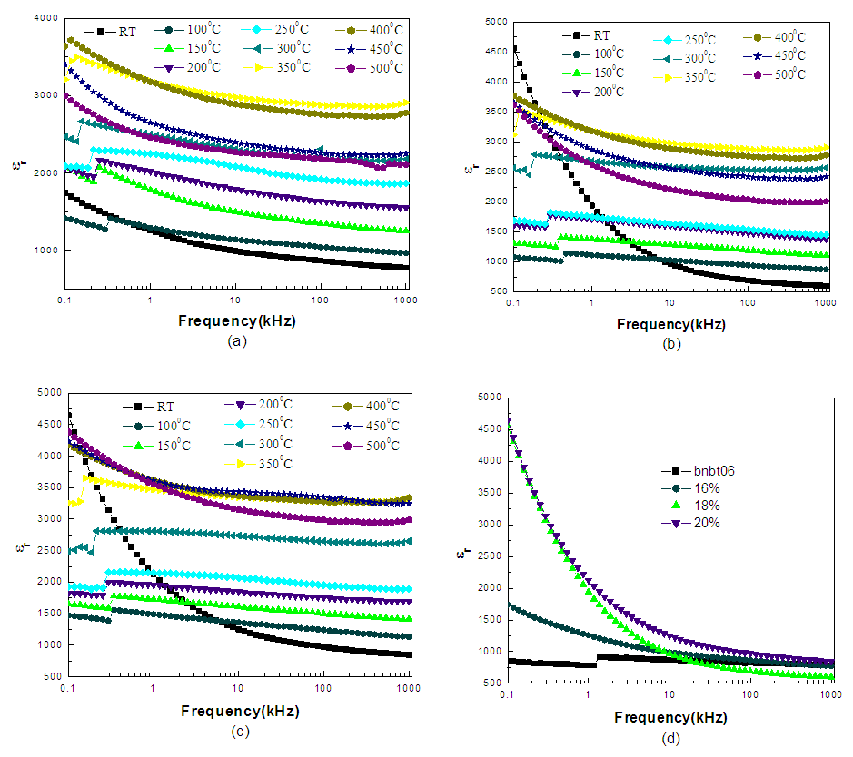 | Figure 3. (a)–(c) Frequency dependence of dielectric constant for BNKxBT6 (x = 0.16, 0.18 and 0.20) ceramics at several temperatures and (d) corresponding plots at RT |
 | Figure 4. (a)–(c) Frequency dependence of tangent loss for BNKxBT6 (x = 0.16, 0.18 and 0.20) ceramics at several temperatures and (d) corresponding plots at RT |
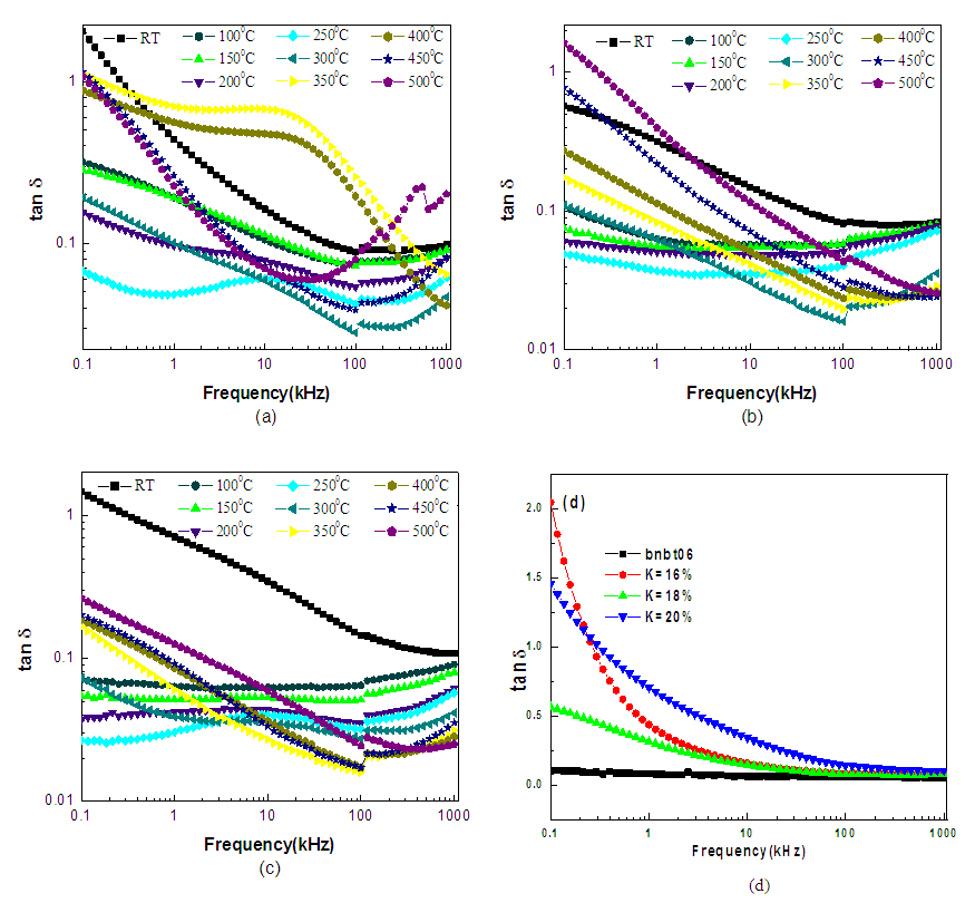
 | Figure 5. Temperature dependence of dielectric constant for BNKxBT6 (x = 0.16, 0.18 and 0.20) ceramics at (a) 1 kHz (b) 10 kHz |
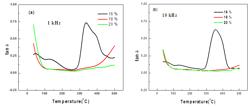 | Figure 6. Temperature dependence of loss tangent for BNKxBT6 (x = 0.16, 0.18 and 0.20) ceramics at (a) 1 kHz (b) 10 kHz |
3.3. Impedance Study
- The ac impedance analysis has been found to be a powerful tool to separate out the grain boundary and grain-electrode effects, which usually are the sites of trap for oxygen vacancies and other defects. It is also useful in establishing space charge polarization and its relaxation mechanism, by aptly assigning different values of resistance and capacitance to the grain and grain boundary effects. A remarkable aspect of the impedance analysis is the option of calculating the different contributions to the conductivity, namely the bulk, grain boundary and grain-electrode contributions. Fig. 7 and 8, respectively, show the Z’(f) and Z”(f) plots for BNKxBT6(x = 0.16, 0.18 and 0.20) ceramics at several temperatures between ambient temperature and 500°C. From the plots it is seen that at lower temperatures Z’ decreases monotonically with increasing frequency up to a certain limiting range (~10 kHz) above which it becomes almost frequency- independent. The higher values of Z’ at lower frequencies and higher temperatures indicate that the polarization in the test material is larger. The temperature at which this frequency-dependent to frequency-independent change of Z’ occurs, varies with frequency in the material composition. This also signifies that the resistive grain boundaries become conducting at these temperatures and that the grain boundaries are not relaxing even at the highest measurement ranges of frequency and temperature. Z”(f) plots showed almost identical monotonically decreasing type of variation up to the same frequency limit ~10 kHz beyond which they merge together at a very low value of Z” to show frequency-independent nature of variation extending up to the highest frequency limit at all the chosen measurement temperatures. It is also seen that the nature of variation of Z’’ with frequency is opposite to that of Z’ for all the doped ceramic compositions. The merger of Z” (as well as of Z’) at higher frequencies for all the temperatures indicates possible release of space charge accumulation at the boundaries of homogeneous phases in the test material under the applied external field. At lower temperatures, monotonic decrease of Z” for all the compositions indicated that at lower temperatures the relaxation is absent in the material system. This means that relaxation species are immobile defects and the orientation effects may be associated. Also, the decreasing magnitudes of Z’ and Z” with increasing frequencies implied that relaxation in the material is temperature-dependent, and that there is no single relaxation time. At 100 Hz, the maximum and minimum values of Z’ are ~0.7859 MΩ and 0.0286 MΩ for the composition having 0.16 and 0.20 mol % of K+ doping in BNBT6, respectively. The corresponding maximum and minimum values of Z’’ are ~0.3841 MΩ and 0.0182 MΩ.
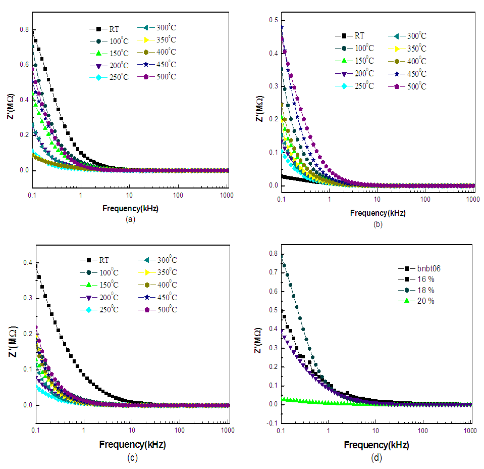 | Figure 7. (a)–(c) Frequency dependence of real part of impedance for BNKxBT6 (x = 0.16, 0.18 and 0.20) ceramics at several temperatures and (d) corresponding plots at RT |
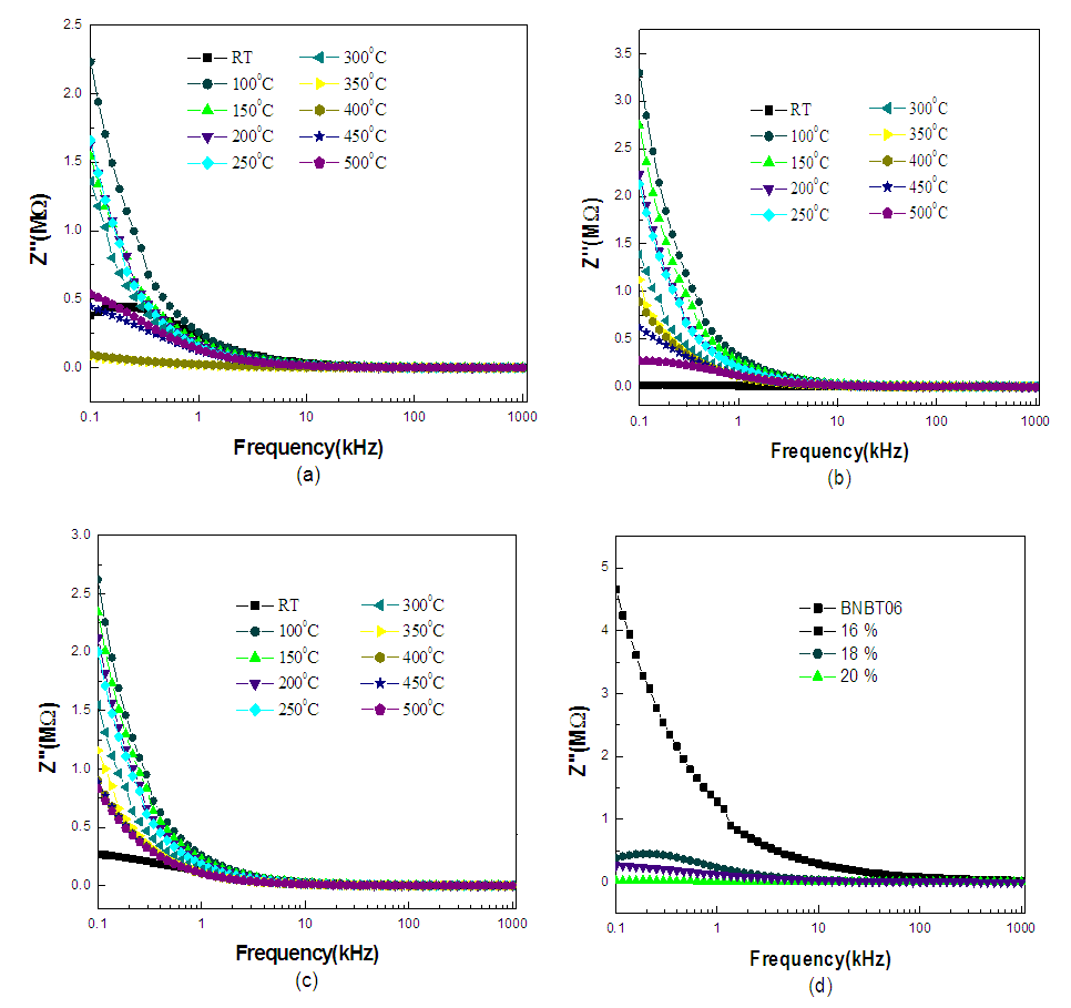 | Figure 8. (a)–(c) Frequency dependence of imaginary part of impedance for BNKxBT6 (x = 0.16, 0.18 and 0.20) ceramics at several temperatures and (d) corresponding plots at RT |
3.4. Complex Impedance Analysis
- Complex Impedance spectroscopy (CIS) is a powerful tool for characterizing many of the electrical properties of materials and their interfaces with electronically conducting electrodes. It may be used to investigate the dynamics of bound or mobile charges in the bulk or interfacial regions of any kind of solid or liquid material: ionic, semiconducting, mixed electronic– ionic, and even insulators (dielectrics). The CIS gives the direct correlation between the response of a real system and an idealized model circuit composed of discrete electrical components. An equivalent circuit based on impedance and electric modulus spectra provides the physical explanation to the processes occurring inside the material system. Most of the real ceramics contain grains and grain-boundary regions, which individually have very different physical properties. These regions are well observed in the impedance and modulus spectra. Electrical ac data may be presented in any of the four interrelated formalism: Relative permittivity (ε*) = ε’- jε”; Impedance (Z*) = Z’+ jZ” = 1/jωC0ε*; Electric modulus (M*) = M’ + jM” = 1/ε*; Admittance (Y*) = Y’ + jY” = jωC0ε*; and tan δ = ε’’/ε’ =M” /M’ = Z’/Z” = Y’’/Y’, where ω(=2πf) is the angular frequency; C0 (= ε0A/t) is the geometrical capacitance; j = √-1; ε0 is the permittivity of free space (=8.854×10⁻¹² Fm−1); t and A are the thickness and area of the pellet, respectively; and δ is complementary to the phase angle (θ), as observed by the LCR Hi-Tester. The electrical properties of the present composite material system have been first investigated using Complex Impedance Spectroscopy (CIS) technique. To study the contribution of various microscopic elements, such as intragrain, intergrain, electrode effect, and relaxation process, Cole-Cole plot analysis was used. Fig. 9 shows the Cole-Cole plots of the compounds corresponding to 425°C, 450°C and 475°C as the measurement temperature. All the resulting curves showed a tendency to bend towards the abscissa to form semicircles with their centers below the real axis, having comparatively larger radii. Further, the radii decrease with the increase of temperature, thereby indicating negative temperature coefficient of resistivity (NTCR) behaviour of the materials, generally found in case of semiconductors and at the same time showing a clear-cut departure from the ideal Debye type behaviour. This non-ideal behavior could be attributed to several factors such as grain orientation, grain boundary, stress-strain phenomena, and atomic defect distribution. However, the ceramic composition having 16mol% of K+ showed the opposite trend of variation as compared with others in the sense that it gave evidence of positive temperature coefficient of resistivity (PTCR) behaviour i.e., dominance of grain boundary compared to that of grains. Complex impedance spectrum is distinguished by semicircles. A series array of two parallel RC combinations [(Rg, Cg), (Rgb, Cgb)] in series with a resistor (Rs) indicate the contribution from grains of the sample in the high frequency region and from the grain boundaries in the low frequency region. No other relaxation mechanism, such as the electrode effects, could be identified through the use of CIS technique in the test frequency and temperature range. Further, it is not possible to get two clearly separated semicircles on the same impedance plot. Fig. 10 shows the Cole-Cole plots of the compounds corresponding to the highest temperature of the measurement i.e. at 500°C. Plots show that the electrical resistivity of the sample decreases as the mole% is increased from 16 to 18, but an opposite trend i.e., representing the increase in resistivity, is shown when the mol% is further increased to 20.
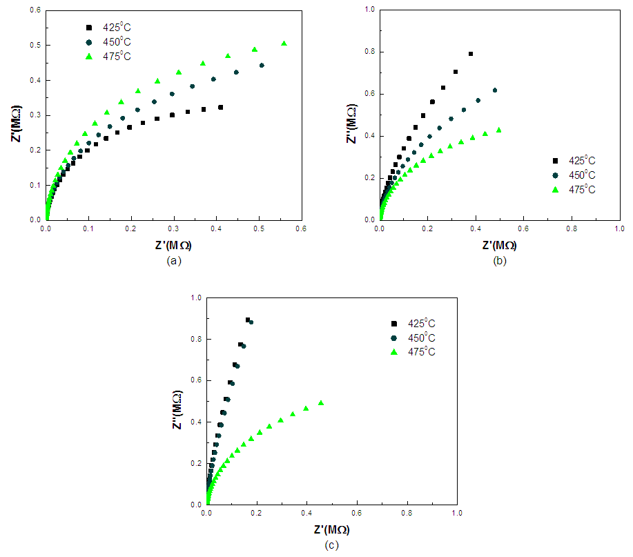 | Figure 9. Complex impedance plots for BNKxBT6 (x = 0.16, 0.18 and 0.20) ceramics |
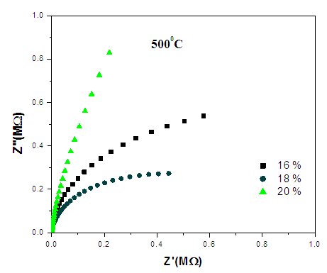 | Figure 10. Complex impedance plots for BNKxBT6 ceramics, measured at 500°C |
3.5. Complex Modulus Analysis
- Complex modulus analysis is an alternative approach to explore electrical properties of the material and magnify any other effects present in the sample (which are unidentifiable or overlapping in CIS technique) as a result of different relaxation time constants. It is an important and convenient tool to determine, analyze and interpret the dynamical aspects of electrical transport phenomena (i.e. parameters such as carrier/ion hopping rate, conductivity relaxation time, etc.). In order to analyze and interpret the experimental data, it is essential to have a model equivalent circuit that provides a realistic representation of the electrical properties. The modulus representation suppresses the unwanted effects of extrinsic relaxation often used in the analysis of dynamic conductivities of ionically conducting glasses. The dielectric modulus (M*=1/ ε*) is frequently used in the analysis of dielectric data of ionic conductors [33]. The advantage of adopting complex electrical modulus spectra is that it can discriminate against electrode polarization and grain boundary conduction processes. Using electric modulus analysis, it is easier to relate this phenomenon to other properties, especially the dynamical mechanical modulus and can be written as a single function of conductivity. Sinclair and West [32, 33] suggested the combined usage of impedance and modulus spectroscopic plots to rationalize the dielectric properties. Only one peak in Z” (f) vs. Z’ (f) plots but two peaks in M” (f) vs. M’ (f) plots at all the test temperatures for all the compositions taken for analysis in the present study suggest that the impedance data can be better analyzed by re-plotting them in the modulus formalism. The peak heights are proportional to R for the Z” (f) vs. Z’ (f) plots and to C−1 for the M” (f) vs. M’ (f) plots. Complex impedance plane plots of Z’’ versus Z’ (where Z’ and Z’’ are the real and imaginary parts of the complex impedance (Z*), respectively) are useful in determining the dominant resistance of a sample but are insensitive to the smaller values of resistances. Similarly, complex modulus plots are useful in determining the smallest capacitance. Thus, the power of combined usage of both impedance and modulus spectroscopy is that the Z’-Z’’ plot highlights the phenomenon of largest resistance whereas M’’ vs. M’ picks up those of the smallest capacitance [38]. The additional contribution in the low frequency part to the specific semicircle is attributed to the blocking effect of the pores. Also the poor separation of the overlapped semicircles is ascribed to the blocker (pore) size and if the blocker size is greater than 1μm, it would lead to the overlapping of the semicircles [39]. Fig. 11 shows the complex modulus plots for BNKxBT6 (x = 0.16, 0.18 and 0.20) ceramics corresponding to the several temperatures i.e., 425°C, 450°C and 475°C. Fig. 12 Shows the complex modulus plots for BNKxBT6 (x = 0.16, 0.18 and 0.20) ceramics corresponding to the highest temperature of measurement i.e. at 500°C. From this figure, we can notice that the samples’ modulus spectrum has a typical semicircular pattern with its centre lying below the real axis, thereby indicating non-Debye type of relaxation response in the investigated material system. In the modulus spectrum, right-side semicircles represent data corresponding to higher frequencies and left semicircles to those corresponding to lower frequencies for each set. These semicircles indicate that both grain and grain boundary capacitance started playing active roles in the conduction mechanism of the material system at higher temperatures.
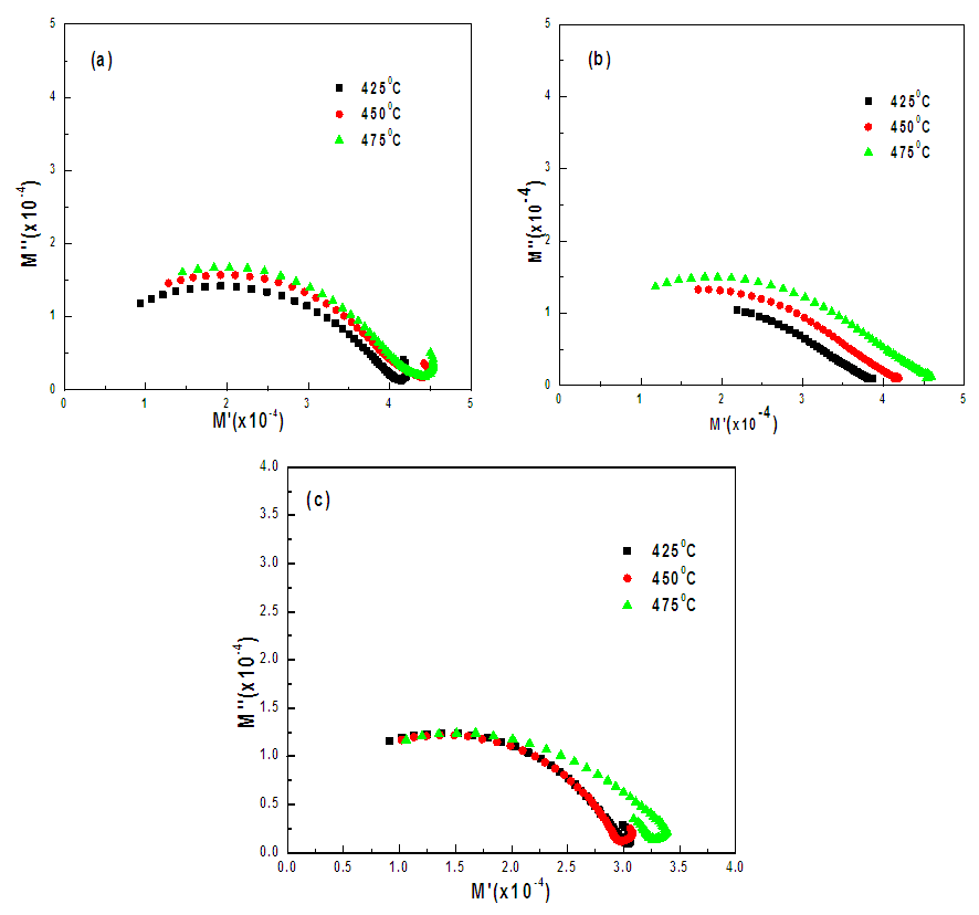 | Figure 11. Complex modulus plots for BNKxBT6 ceramics (x = 0.16, 0.18 and 0.20) ceramics |
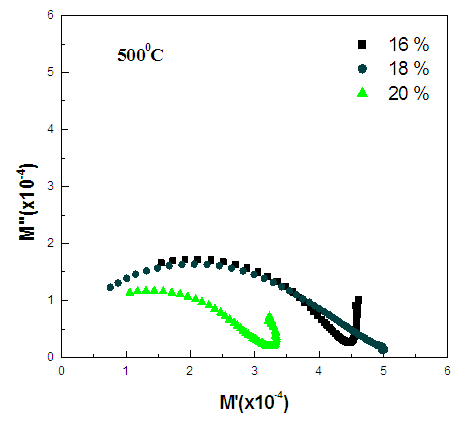 | Figure 12. Complex modulus plots for BNKxBT6 ceramics, measured at 500°C |
4. Electrical Conductivity Analysis
- The real part of AC conductivity
 is directly related to the dielectric properties of the material. Alternatively, the real part of the dominant bulk conductivity may be evaluated from the the impedance spectrum using the relation σ'ac = t / (Z’A); where Z’ is the real part of complex impedance (intersection of semicircle on the real-axis in Z’’ vs. Z’ plot); t the thickness, and A the surface area of the sample. Approximate values of DC conductivity of the test materials were evaluated from the extrapolation of the available plateaus of the σ'ac plots down to ω = 0 for all BNKxBT6 ceramic compositions. Fig. 13 shows the log-log plot of ac electrical conductivity (σac) versus frequency at different temperatures for BNKxBT6 (x = 0.16, 0.18 and 0.20) ceramics. The conductivity spectra have the tendency to merge at higher frequencies with the increase in temperature. At a particular temperature, the conductivity is seen to decrease with decreasing frequency and it becomes independent of frequency after a certain value. The extrapolation of this part towards lower frequency gives σdc which is attributed to the long range translational motion of the charge carriers. This behaviour may be attributed to the presence of space charge in the material. The basic fact about AC conductivity (σac) in this system is that σac is an increasing function of frequency with any type of hopping model taken into account.
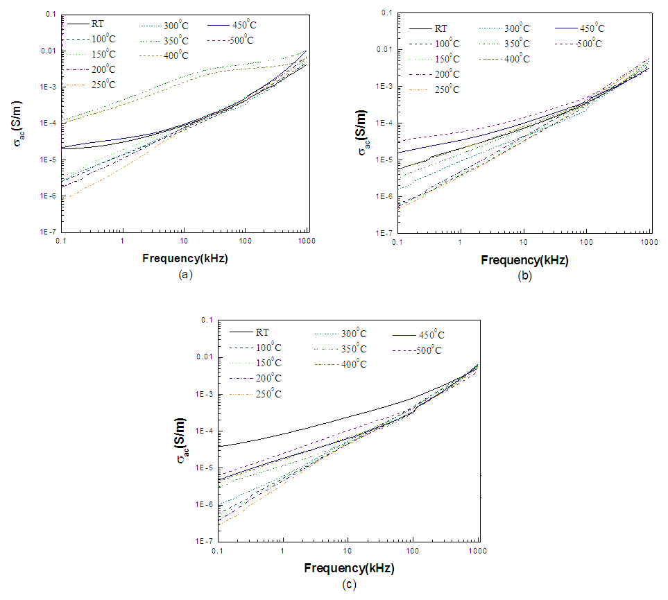 | Figure 13. (a)–(c) Frequency dependence of real part of ac conductivity for BNKxBT6 (x = 0.16, 0.18 and 0.20) ceramics at several temperatures |
 | (2) |
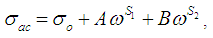
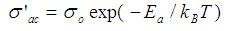
 is the frequency independent (electronic or dc) part of ac conductivity. The exponent s1 (0 ≤ s1 ≤ 1) characterizes the low frequency region i.e., to the grain-boundary conductivity, corresponding to translational ion hopping whereas the exponent s2 (0 < s2 < 2) characterizes the high frequency region i.e., to the grain conductivity indicating the existence of well localized relaxation/re-orientational process [42], the activation energy of which is ascribed to the reorientation ionic hopping. In the jump relaxation model (JRM) introduced by Funke [43] and extended by Elliot [44] to account for ionic conduction in solids, there is a high probability for a jumping ion to jump back (unsuccessful hop). However, if the neighbourhood becomes relaxed with respect to the ion’s position, the ion stays in the new site. The conductivity in the low frequency region is associated with successful hops. Beyond the low frequency region, many hops are unsuccessful and as the frequency increases, there is higher possibility of more hops to be unsuccessful. The change in the ratio of successful to unsuccessful hops results in dispersive conductivity in the test material(s). In the perovskite type oxide materials, presence of charge traps in the band gap of the insulator is expected. The JRM suggests that different activation energies are associated with unsuccessful and successful hopping processes. The frequency response of the conductivity for the test materials endorsed Jump Relaxation Model and conductivity data were found to be fitting in double power law as given in Equation (2). Fig. 14 (a)-(c) shows the ln (σ'ac) vs.1000/T plots for the three compositions i.e., BNKxBT6 ceramics (x = 0.16, 0.18 and 0.20). It is observed from these plots that in the low temperature regime, ac conductivity of all the compositions increased with increase in frequency, however a bit slowly, thereby indicating dispersion of conductivity with frequency. With increase in temperature, dispersion in conductivity narrowed down and all the curves for different frequencies appeared to merge at high temperatures, although they didn’t merge completely.
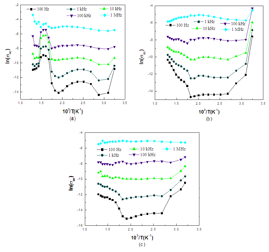 | Figure 14. (a)–(c) Inverse temperature dependence of log of real part of complex AC conductivity (σ'ac) for BNKxBT6 (x = 0.16, 0.18 and 0.20) ceramics at indicated frequencies |
 | (3a) |
 | (3b) |
|
 with increase in temperature decreases i.e., s1 decreases with an increase in temperature. Since the trapped carrier of a large polaron extends over multiple sites, the carrier can continuously adjust to the alternations of the atomic positions and thereby move between sites coherently [45, 46]. Hence, the conductivity increases with the increase in temperature. The value of s2 has also a decreasing trend with increase in temperature beyond 300°C for almost all the compositions. A similar explanation to the temperature-dependent variations of s2, as for s1, also holds good. In the light of the resulting frequency and temperature-dependent AC conductivity data for BNKxBT6 ceramic compositions, it may be inferred that the JRM for the hopping of charge carriers seems to hold good in the entire frequency range for them.
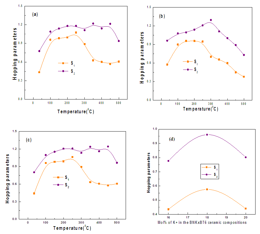 | Figure 15. (a)–(c) Temperature-dependence of low and high frequency hopping parameters (s1 and s2) for BNKxBT6 (x = 0.16, 0.18 and 0.20) ceramics between ambient temperature and 500oC and (d) corresponding plots for different fractions at RT |
5. Conclusions
- Structural, microstructural, dielectric, impedance / modulus and conductivity studies on [Bi0.5(Na1-xKx)0.5]0.94Ba0.06TiO3, (0.16≤ x≤0.20) ceramics in the frequency range 100 Hz-1MHz from the temperature of ambience up to 500°C and the effect of incorporation of K+ on the electrical properties and crystal structure were examined in the present work. The complex impedance and modulus spectroscopy endorsed the grain and grain boundary contributions towards electrical conductivity and presence of non Debye type of relaxation in majority of the test material system. The frequency response of the conductivity for the test materials endorsed Jump Relaxation Model fitting double power law to be applicable to them. Hopping via small as well large polarons is indicated in all the test material compositions. Near the MPB region (i.e. x = 0.18) in [Bi0.5(Na1-xKx)0.5]0.94Ba0.06TiO3 ceramics showed an improvement of electrical properties over those of other compositions. Therefore, BNKxBT6(x=0.18) ceramic seems to be a promising candidate as a new lead-free piezoelectric ceramic which can be further used in actuator applications.
ACKNOWLEDGEMENTS
- The authors gratefully acknowledge the support for the present research work from the Research Project SR/S2/CMP-0017/2008 run in the Univ. Department of Physics, Tilkamanjhi Bhagalpur Univ., Bhagalpur financed by the Dept. of Science &Technology, New Delhi.