S. Bensmaine, B. Benyoucef
Unité de Recherche Matériaux et Energies Renouvelables (URMER). Université de Tlemcen, BP 119, Tlemcen, 13000, Algeria
Correspondence to: S. Bensmaine, Unité de Recherche Matériaux et Energies Renouvelables (URMER). Université de Tlemcen, BP 119, Tlemcen, 13000, Algeria.
| Email: |  |
Copyright © 2012 Scientific & Academic Publishing. All Rights Reserved.
Abstract
In this work, we investigate experimentally the different properties of ZnO thins films deposited by radio-frequency magnetron with Zinc target (sputtering method) and we calculate the frequency peaks in ZnO/SiO2/Si structure. We study the effect of the power and the pressure deposition on the thin films properties. We characterized by X-ray diffraction the film crystalline quality and by scanning electron microscopy (SEM) the film morphology. The X-ray diffraction analyses has revealed that the ZnO film is polycrystalline in nature having a hexagonal wurtzite type crystal structure and (002) orientation. The SEM showed that the structure of the films is columnar. The thickness of the films is measured by profilometer apparatus (Dektak3 ST). The principal application of ZnO thin films is the SAW (surface acoustic wave) devices. We realized experimentally the ZnO/SiO2/Si structure with the optimal parameters. The frequency response of the device is measured by the network analyzer. We obtained the frequency of 476 MHz for a phase velocity of 5712 ms-1.
Keywords:
Thin Films Zinc Oxide, Characterization, SAW Devices, Frequency Peak
Cite this paper: S. Bensmaine, B. Benyoucef, Experimental Characterization of ZnO Thins Films and Identification of Frequency Peaks in ZnO/SiO2/Si SAW Devices, American Journal of Materials Science, Vol. 3 No. 4, 2013, pp. 100-103. doi: 10.5923/j.materials.20130304.06.
1. Introduction
Zinc Oxide is one of the most used thin film piezoelectric material. It belongs to the hexagonal wurtzite crystal type, having 6mm symmetry. This structure can be considered as two inter-inserted hexagonal structures (zinc and oxygen) spaced by (3/8) c from each other, where c is the main symmetry axis of the crystal. It is generally treated as a semiconductor as a result of excessive zinc. ZnO is very versatile and due to its high coupling coefficient, many applications exist, like SAW devices[1], bulk acoustic wave devices, gas sensors, infrared detectors, tactile sensor arrays[2].ZnO can be deposited using various physical and chemical vapour deposition techniques (pulsed-enhanced chemical vapour deposition, pulse laser deposition, ion-beam assisted deposition, molecular beam epitaxy, sputtering…). Radio-frequency magnetron sputtering technique is one of the most widely used to its reproducibility and efficiency[3, 4, 5]. The growth methods of ZnO films are compatible with a wide range of substrates (pyrex, quartz, silicon, sapphire…). ZnO is a wide-bandgap oxide semiconductor with a direct energy gap of about 3.37 eV. The zinc oxide has emerged as one of the most promising materials, due to its optical and electrical properties associated with the high chemical and mechanical stability. The physical properties of the films depend on the sputtering parameters, such as the substrate temperature, the oxygen partial pressure and the sputtering power[6]. Therefore, it is meaningful to report in this paper, the effects of the pressure and power on ZnO thins films structural and morphological properties using r.f. magnetron sputtering. We investigate experimentally with the optimal parameters the ZnO/Si and ZnO/SiO2/Si structures.The ZnO c-axis with respect to the surface normal was showed to be a necessary requirement towards shear wave mode excitation in SAW. The sensing mechanism consists of a perturbation of the surface along which the waves propagate. The frequency characterization of the SAW devices is obtained with a network analyzer and using equation (1)  | (1) |
where f is the measured centre frequency, λ the considered used wavelength (μm) and v the phase velocity calculated.
2. Experimental Details
Various deposition techniques have been for ZnO thin films. Two types are predominant: chemical vapour deposition CVD and physical vapour deposition PVD. Many different kinds of thin films are deposited by evaporation and sputtering, both of which are examples of PVD. This processes for deposition of ZnO thin films use the generation of gaseous phase ZnO molecules from a solid ZnO target and the condensation of these molecules on a substrate. During sputtering, the target (Zn or ZnO) at a high negative potential, is bombarded with positive inert gas ions (mostly Ar) created in plasma. The target material is sputtered away by momentum transfer and the ejected surface atoms are deposited (condensed) onto the substrate placed an anode. Sputtering is preferred over evaporation in many applications due to a wider choice of materials to work with and better adhesion to the substrate[7]. Sputtering is employed in laboratories and production settings. Most sputtered ZnO films are polycrystalline and grow preferentially with their crystallographic c-axis perpendicular to the substrate on any material[8].
2.1. Effect of the Deposition Power and Pressure
The ZnO thin films were deposited by r.f. magnetron system on silicon Si (100) substrates. The Zinc target (purity 99.99%) diameter was 100 mm (4 inch) and 6.35 mm thick. The distance between the cathode and the substrate holder was 70 mm. The deposition chamber was pumped down to a base pressure of 5.10-7mbar by a turbomolecular pump prior to the introduction of the argon-oxygen gas mixture for ZnO thin films production. The RF power delivered by the RF generator was fixed at 20 watts and 100 watts. The pressure was fixed at 2.10-2mbar, 2.10-3mbar and 6.10-3mbar.All these conditions were summarized in table 1 and table 2. Table 1. Deposition conditions of ZnO/silicon structure by magnetron sputtering. Variation of the RF power
 |
| |
|
Table 2. Deposition conditions of ZnO/silicon structure by magnetron sputtering. Variation of the pressure
 |
| |
|
The crystallographic structure of films were analysed by X-ray Diffraction using the Cu Kα (with λ = 1.5405 A°) radiation. The morphology of the films is obtained by using scanning electron microscopy. The profilometer apparatus allows the measurement of the thickness and the growth rate of the ZnO thin films.
3. Results and Discussion
3.1. Structural Properties
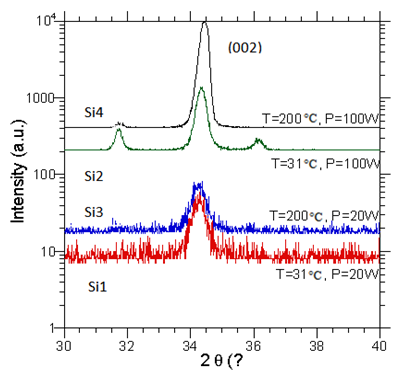 | Figure 1. X-ray diffractograms of ZnO thin films as function of r.f. power with 2.10-2mbar of pressure |
The XRD analyses of the ZnO thin films on silicon are shows in fig.1 As can be seen the samples Si1and Si3 shows a low quality of the crystalline structure of ZnO thin films. It could be attributed to the low RF power delivered by the RF generator. Further increasing substrate temperature and time deposition don’t give a better result. The samples Si2 and Si4 shows on the XRD analyses an important peak (002) oriented ZnO crystallites. These samples have a good crystalline quality. As can be seen the crystalline quality is very sensitive to the RF power[5, 9].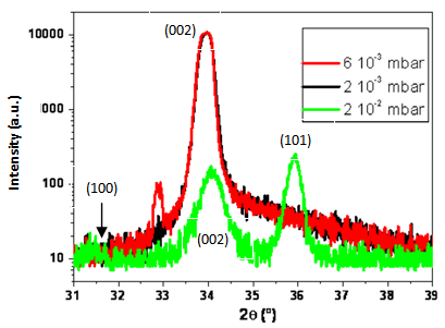 | Figure 2. X-ray diffractograms of ZnO thin films as function of pressure with 100 watt of power |
Fig.2 shows the XRD patterns for samples deposited at several pressures (2.10-2mbar, 2.10-3mbar and 6.10-3mbar). We observe at low pressure of 2.10-3 mbar only one strong peak at 2θ~34.4°, which can be attributed to the (002) line of the hexagonal ZnO wurtzite phase. This sample Si6 is highly textured, with c-axis perpendicular to the substrate surface[10]. It can be explains that the zinc atoms and oxygen atoms undergo fewer collisions, and thus have more kinetic energy, allowing them to arrange to form the plan (002). The intensity of the (002) peak decreases at high pressure of 2.10-2 mbar. The three peaks at the higher pressure of 2.10-2 mbar correspond to (100), (002) and (101) orientations and their relatively low intensities indicate a poor crystalline quality because the atoms suffer more collisions and therefore have less kinetic energy. Moreover the peak intensity decreases while its full width at half maximum (FWHM) increases.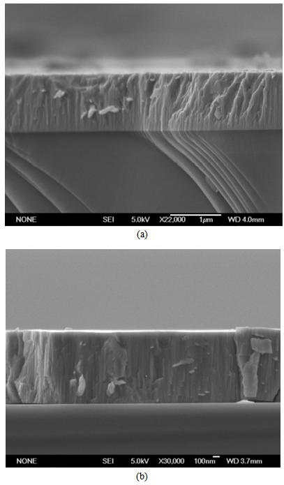 | Figure 3. Typical image of c-axis ZnO film on silicon. (a) : at 100watts RF power and 200°C temperature substrate Si4. (b) : at a pressure of 2.10-3mbar Si6 |
The cross sectional micrograph of c-axis ZnO thin films shows a columnar growth structure, fig.3. The image presents polycrystalline ZnO thin films growth with their c-axis perpendicular to the silicon substrate.
3.2. Thickness and Growth Rate
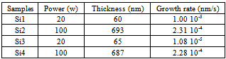
The thickness of the films and the growth rate are summarised in the table 3. For each sample, we have measurements the thickness of the ZnO thin films using the (Dektak3 ST) apparatus. Table 3. Thickness and deposition rate for different samples Si1, Si2, Si3 and Si4
 |
| |
|
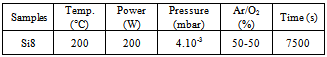
As can be seen when the RF power decreases, the thickness of the thin films decrease, which explains the decreasing of the growth rate. We observe that at 100 watts RF power, we obtained a bigger growth rate so an important flow of Zinc, consequently, the decrease of the time for reaction of the oxygen on the surface of the thin films. We conclude that increasing the RF power can density the ZnO thin films. All these characterizations have permitted us to choose good deposition parameters, which are summarized in table 4.In order to increase the roughness of the silicon substrate for ZnO thin films growth, we use an amorphous SiO2 film. The SiO2 deposition conditions were: the chamber pressure at 6×10⁻³ mbar, the substrate temperature at 39 °C, the argon-oxygen gas mixture at (20 sccm/20 sccm), the r.f power at 100 W and the time of deposition was fixed at 720 s.Table 4. Deposition conditions of Zinc Oxide by magnetron sputtering
 |
| |
|
4. Application as SAW Devices
4.1. Frequency Peak Determination
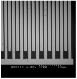 | Figure 4. SEM image of a completed IDTs |
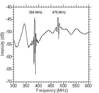 | Figure 5. The frequency response of the SAW device fabricated on a structure ZnO/SiO2/Si |
To check the piezoelectricity of the ZnO thin films, a SAW device was performed on a structure ZnO/SiO2/Si. Fig. 4 shows SEM image of a completed IDTs (inter-digital transducers). We have used the network analyzer for the frequency response of the device[11]. We have obtained the result shows in Fig. 5, which presents the insertion loss (dB) versus frequency (MHz).Fig. 5 shows the frequency response of the SAW device taken between 300 and 600 MHz. The two peaks correspond to the mode of propagation. The first peak corresponds to a frequency of 384 MHz for a phase velocity equal to 4608 m.s-1 and the second peak corresponds to the frequency of 476 MHz for a phase velocity of 5712 ms-1.
5. Conclusions
In summary, we have deposited ZnO films by r.f magnetron system on silicon (100) substrates. We have observed that the crystalline quality improves with the increase of the injected RF power because there is more to create reactive species, such as argon ion. We have observed that increasing the power is used to obtain a good crystalline quality of the thin films because the atoms undergo fewer collisions and can have a better kinetic energy. The crystalline quality of the sample is small, in view of low power and even if you double the deposition time and increases the deposition temperature. The crystalline orientation of ZnO films is strongly influenced by the deposition pressure. So, the ZnO film deposited at low operating pressure of 2x10⁻³ mbar shows a single orientation (002) corresponding to the c-axis perpendicular to the substrate. With the optimal deposition conditions, we have fabricated a SAW device with a ZnO/SiO2/Si structure. The best frequency of 476 MHz is obtained for a phase velocity of 5712 ms-1 and 12 μm wavelength.
References
| [1] | Ki Hyun Yoon, Ji-Won Choi,Dong-Heon Lee, Thin Solid Films 302 (1997)116-121. |
| [2] | Y. E. Lee, J. B. Lee, Y. J. Kim, H. K. Yang, J. C. Park, H. J. Kim, J. Vac. Sci. Technol. A 14, 1943 (1996).J. Breckling, Ed., The Analysis of Directional Time Series: Applications to Wind Speed and Direction, ser. Lecture Notes in Statistics. Berlin, Germany: Springer, 1989, vol. 61. |
| [3] | M. Link, M. Schreiter, J. Weber, R. Gabl, D. Pitzer, R. Primig, and W. Wersing ,M. B. Assouar, O. Elmazria, Journal of Vacuum Science & Technology A: Vacuum, Surfaces, and Films 24 (2006) 218. |
| [4] | A. Mosbah, A. Moustaghfir, S. Abed, N. Bouhssira, M.S. Aida, E. Tomasella and M. Jacquet, Surface and Coatings Technology, 200 (2005) 293. |
| [5] | S. Bensmaine, L. LeBrizoual, O. Elmazria, B. Assouar, B. Benyoucef, Journal of Electron Devices, Vol. 5, (2007), pp. 104-109. |
| [6] | Y. Yoshino, T. Makino, Y. Katayama, T. Hata. Vacuum 59, 538, (2000). |
| [7] | M. J. Madou, Fundamentals of Microfabrication, CRC Press, Bacaraton, FL (2002). |
| [8] | J. G. E. Gardeniers, Z. M. Rittersma, G. J. Burger, J. Appl. Phys. 83, 7844 (1998). |
| [9] | Y. Yoshino, T. Makino, Y. Katayama, T. Hata, Vacuum 59, 538 (2000). |
| [10] | L. LeBrizoual, T. Lamara, F. Sarry, M. Belmahi, O. Elmazria, J. Bougdira, M. Rémy, P. Alnot, Physica Status Solidi (a), vol202/11, p.p 2217-2223 (2005). |
| [11] | S. Bensmaine, L. LeBrizoual, O. Elmazria, J.J. Fundenberger, M. Belmahi, B. Benyoucef. Diamond and Related Materials. Vol 17, p.p 1420–1423 (2008). |
 Abstract
 Reference
 Full-Text PDF
 Full-text HTML