Benjamin Victor Odari1, Robinson Juma Musembi2, Maxwell Joel Mageto1, Herick Othieno3, Francis Gaitho1, Mwamburi Mghendi4, Valentine Muramba1
1Department of Physics, Masinde Muliro University of Science and Technology, P.O Box 190, 50100, Kakamega, Kenya
2Department of Physics, University of Nairobi, P.O Box 30197-00100, Nairobi, Kenya
3Department of Physics, Maseno University, P.O Box Private Bag, Maseno, Kenya
4Department of Physics, University of Eldoret, P.O Box 1125, Eldoret, Kenya
Correspondence to: Benjamin Victor Odari, Department of Physics, Masinde Muliro University of Science and Technology, P.O Box 190, 50100, Kakamega, Kenya.
| Email: |  |
Copyright © 2012 Scientific & Academic Publishing. All Rights Reserved.
Abstract
F-co-doped Palladium Tin Oxide (PTO) thin films were pyrolytically deposited on glass substrate at 4500C using an alcoholic precursor solution consisting of Tin (IV) Chloride (SnCl4.5H2O), Palladium Chloride (PdCl2) and Ammonium Fluoride (NH4F). A resistivity of 0.3-6.9×10⁻²Ωcm was obtained in F-co-doped PTO films prepared with a Pd content of 3.68at% and F content of 0 – 23.96at% under optimized conditions. The optical properties were studied in the UV/VIS/NIR region. The optical bandgap of the films laid in the range 3.945 – 4.014 eV. Using dispersion analysis with Drude and Kim terms, optical constants were determined from spectro-photometric measurements for films on glass.
Keywords:
Spray Pyrolysis, Tin Oxide, Codoping, Fluorine and Palladium Doping, Electrical, Optical
Cite this paper: Benjamin Victor Odari, Robinson Juma Musembi, Maxwell Joel Mageto, Herick Othieno, Francis Gaitho, Mwamburi Mghendi, Valentine Muramba, Optoelectronic Properties of F-co-doped PTO Thin Films Deposited by Spray Pyrolysis, American Journal of Materials Science, Vol. 3 No. 4, 2013, pp. 91-99. doi: 10.5923/j.materials.20130304.05.
1. Introduction
Transparent conducting oxide (TCO) films produced using binary compounds such as SnO2, In2O3 and ZnO doped with an impurity are in practical use[1]. Doped SnO2 is used in a wide range of applications which include the field of sensors, opacities, transparent electrodes in solar panels and other electrochromic devices, thin film magnetic recording media and as material for Li-ion batteries[2, 3]. However, these developments require improvements in electrical, optical and chemical properties of SnO2 thin films used. New transparent conducting oxide films using ternary compounds such as Zn2SnO4, ZnSnO3, MgIn2O4, Zn2In2O5 and In4Sn3O12 have been reported[1]. In addition to the use of ternary compounds, multicomponent oxides such as ZnO-In2O3, In2O3-SnO2, Zn2In2O5-In4Sn3O12 and MgIn2O4-Zn2In2O5 were proposed[1]. The use of ternary and multicomponent oxides whose physical and chemical properties can be controlled by changing their chemical compositions, may be used to improve the properties of SnO2 and its applications. SnO2 film is highly transparent in the visible region, chemically inert, mechanically hard and can resist high temperatures[4, 5, 6] as it is only attacked by hot concentrated alkalis[3]. It belongs to a class of materials that combines high electrical conductivity with optical transparency and therefore constitutes an important component for the optoelectronic applications[2]. The efficiency in these applications is usually improved by suitably doping the tin oxide for example, doping with Sb and F increases the conductivity of tin oxide[3, 7, 8, 9]. Tin oxide is a crystalline solid with a tetragonal crystal lattice. It is a wide gap, non-stoichiometric semiconductor and behaves as a degenerate n-type semiconductor with a low resistivity ( Ωcm)[9]. It can exist in two structures belonging to an indirect band gap of about 2.6 eV[10] and direct band gap that ranges from 3.6 eV to 4.6 eV at room temperature[9,11]. Studies have shown that F doped SnO2 films have higher electrical conductivity, optical transmission and infrared reflection than the tin oxide films prepared with other dopants[7] while Pd doped SnO2 films have high sensitivity to reducing gases when used as metal gas sensors[12]. Some of the most popular methods of depositing Tin oxide thin films include the following: Plasma enhanced Chemical Vapour Deposition[2], Electron beam Evaporation[6], Reactive sputtering[13], Sol-gel[14], Electronspun[15], Inkjet printing[16] and Spray pyrolysis[4, 5, 7, 12]. Of these methods the spray pyrolysis method represents the less expensive method since it can produce large area, high-quality and low cost thin films[7]. It is also suitable for substrates with complex geometry and can be used for a variety of oxide materials[17]. A previous study[30] has shown that the co-doping of SnO2 based ceramics with Sb5+ and Zn2+, noticeably enhances the properties of SnO2 by combining the advantages of Sb5+ which increases the electrical conductivity and Zn2+ which greatly improves the ceramic density.In the present study, we report on the deposition and the characterization of single and co–doped SnO2 thin films prepared by spray pyrolysis technique for optoelectronic applications. The aim of this work is to give an insight on how fixed deposition conditions influence the optical and electrical properties of the produced films with a thickness of 132.5±10 nm. The optical characteristics (transmittance and reflectance) have been evaluated in the UV–Vis–NIR spectral range. In addition, calculations have been carried out in order to determine the carrier densities as well as the optical mobilities by using the Drude model.
2. Experimental
2.1. Sample Preparation
The substrates used were ordinary float glass slides which were 1.2 mm thick and measuring 2.5 by 7.6 cm2. The cleaning procedure involved rubbing the glass slides gently on both sides using a cotton swab soaked in foam made from a mixture of deionized water, liquid detergent and sodium hydroxide in the ratio of 3:2:1. They were then drag wiped using a lens cleaning tissue held at an angle of 45 degrees before being wiped with Isopropyl alcohol and acetone respectively. Lastly, the substrates were ultrasonically cleaned in distilled water for 30 minutes before drying with spray of pressurized air. Spray pyrolysis technique was used to deposit the films at a substrate temperature of 450±10℃ using compressed air at 1 bar as the atomization gas. The experimental set up of the in-house-made spray pyrolysis system is as shown in Figure 1. It consisted of a fume chamber, hot plate, spray nozzle of diameter ~1mm, input gas valve, gas compressor, gas flow meter, conduit tube, thermocouple and pressure gauge. SnO2 films were produced from a precursor solution consisting of Tin (iv) chloride (99%) prepared by dissolving completely 6g of stannic chloride in 100ml of ethanol (99.9%)[3,5,6].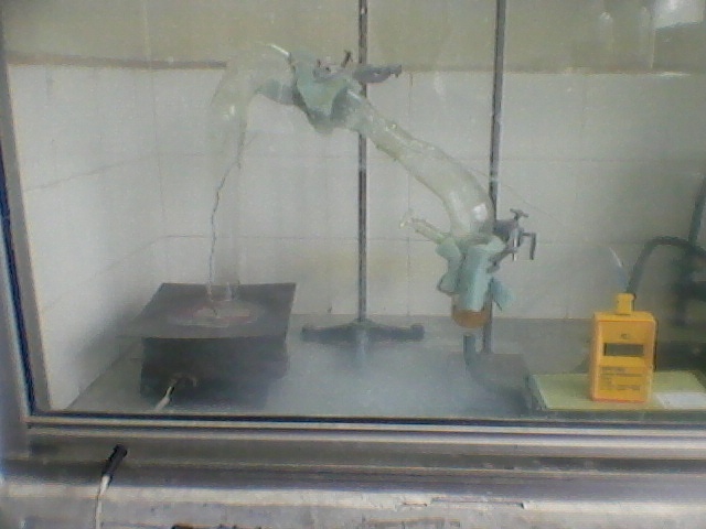 | Figure 1. Spray pyrolysis setup |
The PTO films were prepared by dissolving PdCl2 (59-60%Pd) in ethanol (99.9%) then added to the spraying solution at a constant volume. For F:PTO films, varying volumes of a solution of 0.5g NH4F (99%) in distilled water was added to the starting solution[16,18].The spraying was done under the following conditions:● Substrate temperature: 450±10℃● Carrier-gas: Compressed air at 1 bar● Solution flow rate: 6ml/min● Nozzle-to-substrate distance: 33cm horizontally 32+3cm verticallyAfter spraying, the films were left to cool with the hot plate before removal for transmittance and reflectance measurements.
2.2. Sample Characterization
Spectral normal transmittance T(λ) and near normal reflectance R(λ) were measured in the wavelength range 300 < λ < 2500nm, on a computerized double beam solid-spec 3700DUV Shimadzu Spectrophotometer equipped with 198851 Barium Sulphate (BaSO4) integrating sphere. Barium Sulphate plate was used as a reference for the calculation of optical properties such as band gap, absorption coefficient and refractive index. The thickness of the as-deposited samples of F:PTO were estimated by fitting the experimental spectral data to theoretical spectral data based on Drude and Kim analysis using the SCOUT software[19] in the wavelength range 300nm – 2500nm. Electrical resistivity of the films was calculated from two adjustable parameters of Drude: plasma frequency Ωp and damping constant γ.
3. Results and Discussion
3.1. Analysis of Optical Properties
In order to compare the transparency of PTO thin films with various F-doping levels, the optical spectra in the UV-VIS-NIR region and near infrared region of the samples were measured. The optical transparency of PTO films and F:PTO films for both experimental and computed spectral are shown in Figure 2. The films exhibited high transparency in the visible region with an average transmittance of 83%. Maximum transmittance of 85% for 19.11at% F:PTO at wavelength of 540nm was recorded. The two weird peaks at about 900nm and 1600nm occur due to change of detectors since the SolidSpec-3700DUV spectrophotometer used in this study, is equipped with 3 detectors: a photomultiplier tube detector for the ultraviolet and visible regions, and InGaAs and PbS detectors for near infrared region. The photomultiplier tube detector can be switched to the InGaAs detector in the wavelength range from 700nm to 1000nm (the default switching wavelength is 870nm). The InGaAs detector can be switched to a PbS detector in the range from 1600nm to 1800nm (the default switching wavelength is 1650nm).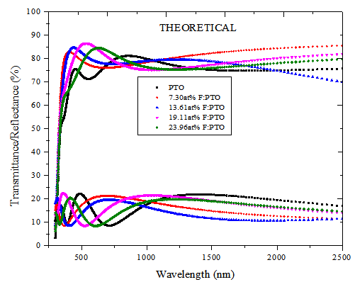 | Figure 2(a). Experimental Spectral Transmittance and Reflectance of PTO film and F:PTO films of thickness 132.5 ± 10 nm prepared at 450±10℃ |
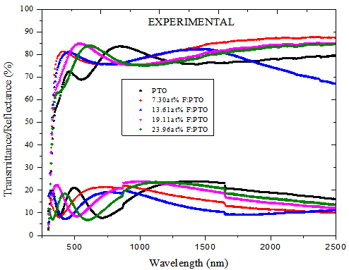 | Figure 2(b). Computed Spectral Transmittance and Reflectance of PTO film and F:PTO films of thickness 132.5 ± 10 nm prepared at 450±10℃ |
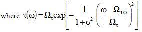
The transparency at wavelengths of 355 – 495nm had a maximum of 81.7% for 7.30at% F:PTO which decreased with increasing F doping concentration to 64.2% for 23.96 at % F:PTO. This is due to the increase in fundamental absorption as photon striking increases with increase in carrier concentration[20]. The maximum transmittance observed in the 19.11at% F:PTO films may be attributed to a decrease in diffuse and multiple reflections caused by the increase in grain size and a reduction in light-scattering effect[21]. The film with the lowest resistivity had the lowest transmission, especially in the near infrared. A sharp fall in transmission at about 310 nm is due to the absorption of the glass substrate[14].The optical constants are reported in Figure 3 showing spectral refractive index n(λ) and extinction coefficient k(λ) for PTO film and F:PTO films. Dispersion analysis using a model for the dielectric susceptibility of the film consisting of Drude[22] and Kim terms[23] was used to model the measured reflectance and transmittance. The charge carriers set free by the donors or acceptors can be accelerated by very little energies and hence do respond to applied electric fields with frequencies in the infrared region[19]. Drude is a free electron contribution which describes the intraband contributions to the optical properties.This model has two adjustable parameters: plasma frequency,  and damping constant,
 . The plasma frequency is proportional to the square root of the carrier density and the damping constant is proportional to the inverse of the mobility. The Drude dielectric susceptibility
 , expressed as a function of frequency ω, is given as[19, 22]
 | (1) |
The one oscillator contribution developed by Kim contains four adjustable parameters:  resonance frequency,
  oscillator strength,
  damping constant and Gauss–Lorentz-switch constant
  .
.  may vary between zero and infinity. For
  = 0, a Gaussian line shape is achieved. A large value of
  (larger than 5) leads to a Lorentzian line shape. The Kim oscillator models the weak broad interband absorption in the measured wavelength range. The interband dielectric susceptibility described by Kim is given by[20];
 | (2) |
 | (3) |
Model parameters were determined from the best fit between computed and experimental data using Scout software[19]. The best fit gives us directly the optical constants of the film under study. Figure 4 shows the experimental spectra and the fitted simulated spectra of 7.30at% F:PTO. The thicknesses of the five samples obtained from fitting the experimental spectral data to theoretical spectral data based on dispersion analysis using the SCOUT software in the wavelength range 0.3 - 2.5 μm was found to be 132.5 ± 10 nm. This was verified by the thicknesses obtained from SEM cross sections. The thicknesses obtained from the two different methods agree within a discrepancy of not more than 5%.In Figure 3, the refractive index of PTO was found to be around 1.98 at 500 nm. It was also observed that the refractive index of all the films decreases with wavelength and then attains almost a constant value towards higher wavelengths[6].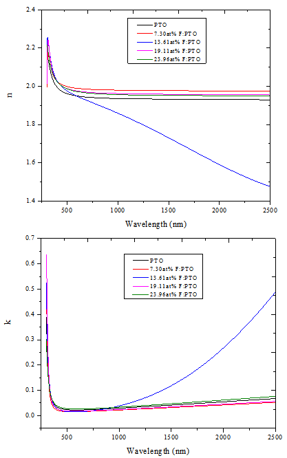 | Figure 3. Spectral refractive index (n) and extinction coefficient (k) of PTO film and F:PTO films prepared at 450±10℃ |
For 13.61at% F:PTO film, refractive index decreased further with increase in wavelength due to the increase in free charge carriers[19].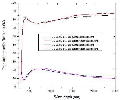 | Figure 4. Best fit curve of Experimental and Simulated spectra from Scout software for 7.30at% F:PTO |
Figure 5 shows spectral absorption coefficient (α) for PTO and F:PTO with four fluorine doping levels. For all the films, the absorption edge lies in the UV region and varies with the charge concentration. The samples show a slight decrease in the absorption coefficient for α < 104 cm-1 for λ > 1000 nm for all samples apart from 13.61at% F:PTO film which tends to increase as shown in Figure 5(i). The dependence on α on hν region is shown in Figure 5(ii). It is clear that the value of α increases with increasing photon energy in the range 0.5 eV – 1.3 eV but decreases for 13.61at% F:PTO film. This may be due to variation in fluorine concentration in the films.The optical bandgap, Eg, was determined using the standard formula[22,23]: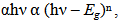 | (4) |
 | Figure 5. Absorption coefficient (α) against wavelength (i) and Absorption coefficient (α) against Energy of PTO film and F:PTO films prepared at 450±100C |
Figure 6 shows plots of (αhν)2 versus photo energy, hν, in the high absorption region. Extrapolation of the curve to hν = 0 gave the direct band gap of PTO and F:PTO films in the range 3.945 eV – 4.014 eV. The bandgaps for 7.30at% Where α=2𝜋k/λ is the absorption coefficient, hν, the photon energy, and n=1/2 accounts for the fact that the directly allowed transitions across the bandgap are expected to dominateF:PTO and 13.61at% F:PTO films are found to be wider than that of PTO, 19.11at% F:PTO and 23.96at% F:PTO. The increase in the energy gap is correlated with the Moss-Burstein effect and many body effects since the absorption edge of the films shifts to shorter wavelength[1]. It shows that Eg, for the transparent thin film, increases with the carrier concentration. There is a good agreement with literature where the values are varying between 3.9 and 4.5 eV depending on the dopants and preparation method[26–29].This indicates an optimum level of Fluorine doping on the PTO film, causes a widening effect on the band gap and is attributed to be due to the gradual increase in carrier concentration and mobility[20,21].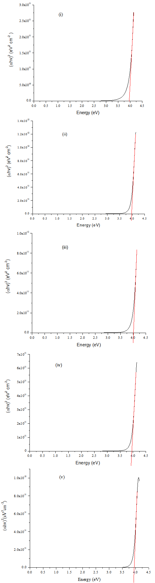 | Figure 6. Energy bandgap of PTO and F:PTO films prepared at 450±10℃, (i) PTO (ii) 7.30at% F:PTO (iii) 13.61at% F:PTO (iv) 19.11at% F:PTO (v) 23.96at% F:PTO |
Figure 7 shows the bandgap energy of PTO thin film and F:PTO thin films with different atomic percentage of F. It is observed that the band gap energy increases with F percentage up to 13.61at% F:PTO then it decreases with increase in the concentration of F. This is in accordance with the findings of Mageto et.al, 2012 and Fatema et.al, 2011[17, 24]. This is due to the decrease in the number of charge carriers for higher F doping concentrations.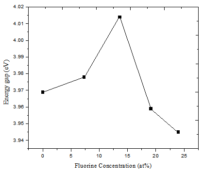 | Figure 7. Energy gap versus F concentration |
3.2. Analysis of Electrical Properties
Electrical properties were analyzed by use of Drude model basing on the results from the spectrophotometer. The polarization P induced by an externally applied electric field E, of the probing light wave in a homogeneous material is given by the electric susceptibility χ; | (5) |
The dielectric function ε connects the dielectric displacement and the electric field vector and is closely related to the susceptibility χ; | (6) |
where | (7) |
The frequency dependence of the susceptibility is very characteristic for a material since it incorporates vibrations of the electronic system and the atomic cores as well as contributions from free charge carriers. The doping of semiconductors leads to free charge carriers which can be investigated by IR spectroscopy. The response of the free carriers to oscillating electric fields can be described to a good approximation by the Drude model. The parameters of that model relate the concentration of the charge carriers and their mobility to properties of the dielectric function. After a model parameter fit of the simulated spectrum to measured data the carrier concentration and the mobility or resistivity can be computed[19]. The Drude model relates the macroscopic susceptibility to the microscopic quantities carrier concentration n and mobility μ;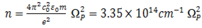 | (8) |
and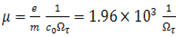 | (9) |
where e is the elementary charge(1.6×10⁻¹⁹C), εo is the permittivity of the free space (8.854×10⁻¹² As/Vm) and m the effective mass of the charge carriers (m=0.3mo)[25] and is the mass of an electron. Resistivity can also be computed using the formula[16];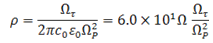 | (10) |
Figure 8 shows resistivity and carrier concentration as a function of the F content for PTO and F:PTO films with F content of 0 – 23.96at%. The distribution of resistivity is mainly related to that of carrier concentration. In particular, the resistivity markedly increased as the F content was increased from 0at% and reached a maximum at a F content of 7.30at%. It then decreased rapidly as the F content was further increased, reaching a minimum at a F content of 13.61at%. | Figure 8. (i) Resistivity versus F Concentration (ii) Carrier concentration versus F Concentration |
The carrier concentration initially decreased as the F content was increased to 7.30 at%. It is well known that a free electron acting as a carrier in SnO2 films is caused by two kinds of donors: a native defect such as an oxygen vacancy and a F- ion on a substitutional site of an O2- ion[17, 18]. Therefore, the drastic decrease of carrier concentration obtained in F:PTO films prepared with F content of 7.30 at % is possibly related to the following two origins: oxidation enhancement of films and carrier compensation due to doped Pd acting as an acceptor. The former may be caused by the spraying process being done in a fume chamber where oxygen is uncontrolled. Consequently, the decrease of carrier concentration may be caused by either extinction of oxygen vacancies or free electron trapping due to the adsorption of oxygen on the grain boundary and/or the surface of films. The latter, carrier compensation due to doped Pd acting as an acceptor, may be explained by the doping of Pd into SnO2 which may cause carrier compensation when a Pd2+ ion occupies the site of an SnO4+ ion. Although the decrease of carrier concentration with increases of F content up to 7.30at% can be explained by a mechanism where Pd acts as an acceptor, it may be difficult to apply this explanation for higher fluorine doping concentrations. In addition, if Pd acts as an acceptor, it is difficult to account for the increase of carrier concentration and its high value observed for films prepared with F contents above 7.30at%, as shown in Figure 7. We suggest that this observed increased carrier concentration with a high value is related to the formation of ternary compounds, for example, F2SnO composed of 2F and SnO[18] and PdSnO composed of Pd and SnO[12]. It has been reported that F: SnO2 films prepared by spray pyrolysis exhibit a high carrier concentration[20]. As described above, the drastic increase of resistivity may be explained by both oxygen enhancement and Pd acceptor mechanisms.
4. Conclusions
Highly transparent and conductive F-co-doped PTO thin films (1.4~2.67×10²Ω-1cm-1) were prepared with a fluorine concentration of 0 – 23.96at% by spray pyrolysis technique from SnCl4 precursor solution. The resistivity of the co-doped films initially increased from 5.14×10⁻² Ωcm with increase in fluorine (7.3at% F:PTO) to attain a maximum value of 6.92×10⁻²Ωcm and drastically decreased to 3.74×10⁻³ Ωcm for higher level doping (13.61at% F:PTO) before gradually increasing again with increase in fluorine concentration. The resistivity achieved for the films doped with 13.61at% F:PTO is the lowest for these films from SnCl4 precursor. Initial codoping of PTO with Fluorine leads to the widening of the bandgap (3.969 - 4.014 eV ) which decreases on further increase of fluorine concentration to 3.945 eV. This is due to the increase in dopant concentration. The average transmittance of the F:PTO films in the visible region was 83%. Increase in fluorine concentration also leads to decrease in transmittance in the visible wavelengths with high transmittance of the 19.11at% F:PTO found to be 88%.
ACKNOWLEDGEMENTS
The authors would like to thank the National Council of Science and Technology, Kenya, for their financial support towards carrying out this research. We also acknowledge the support from University of Nairobi technical team, Mr. Bonface Muthoka, Mr. Dickson Omucheni, Miss Everline Akinyi; and Miss Antonnette Omukaga, for their continuous assistance when carrying out the experiments.
References
| [1] | Tadatsugu M, Takashi Y, Yukinobu T, Toshihiro M. Transparent conducting zinc-co-doped ITO films prepared by magnetron sputtering. Thin Solid Films. 2000; 373:189-194 |
| [2] | Young SK, Ansari SG, Ansari ZA, Rizwan W, Hyung-Shik S. A simple method to deposit palladium doped SnO2 thin films using plasma enhanced chemical vapor deposition technique. American Institute of Physics, Rev. Sci. Instrum. 2010; 81: 113903 |
| [3] | R. Díaz. Tin oxide thin films: electronic properties and growth mechanism under electrochemical control. University of Barcelona, Barcelona, Spain. (2002). |
| [4] | Chitra A, Takwale MG, Bhide VG, Shailaja M, Kulkarni SK. Effect of Sn incorporation on the growth mechanism of sprayed SnO2 films. American Institute of Physics, J. Appl. Phys. 1991; 70: 7382 |
| [5] | Mishra RL, Sheo KM, Prakash SG. Optical and gas sensing characteristics of tin oxide nano-crystalline thin film. Journal of Ovonic Research. 2009; . 5:4: 77 - 85 |
| [6] | Shamala KS, Murthy LCS, Narasimha KR. Studies on tin oxide films prepared by electron beam evaporation and spray pyrolysis methods. Indian Academy of Sciences, Bull. Mater. Sci. 2004; 27: 3, 295–301 |
| [7] | Shadia JI, Riyad NAB. Effect of Processing on the Electrical Properties of Spray-Deposited SnO2:F Thin Films. American Journal of Applied Sciences. 2008; 5 (6): 672-677 |
| [8] | Jebbari N, Kamoun NT, Bennaceur R. Effect of SnCl4 concentration on SnO2:F, deposited by chemical spray pyrolysis. International Renewable Energy Congress, Sousse, Tunisia. 2010 |
| [9] | Agashe C, Marathe RB, Takwale GM, Bhide GV. Structural properties of SnO2:F films deposited by spray pyrolysis technique. Thin Solid Films. 1988; 164: 261-264 |
| [10] | Mohammad TM. Performance and characteristics of Al-PbS/SnO2:F selective coating system for photothermal energy conversion. Solar Energy Mater. 1990; 20:297-305 |
| [11] | Rakhshani EA, Makdisi Y, Ramazaniyan A.H. Electronic and optical properties of fluorine-doped tin oxide films. J. Applied Phys. 1998; 83: 1049-1057 |
| [12] | Boshta M, Mahmud FA, Sayed MH. Characterization of sprayed SnO2: Pd thin films for gas sensing applications. Journal of Ovonic Research. 2010; 6 (2): 93 - 98 |
| [13] | Stanislav R, Ekaterina R, Tamara S. Electrophysical Properties of Gas Sensitive Films SnO2 Doped with Palladium, Sensors & Transducers Magazine. 2004;.40 (2):145-151 |
| [14] | Sandipan R, Gupta PS, Gurdeep S. Electrical and Optical properties of sol-gel prepared Pd-doped SnO2 thin films: Effect of multiple layers and its use as room temperature methane gas sensor. Journal of Ovonic Research. 2010 February; 6(1): 63-74 |
| [15] | Joong-Ki C, In-Sung H, Sun-Jung K, Joon-Shik P, Soon-Sup P, Unyong Jeongc et.al. Design of selective gas sensors using electrospun Pd-doped SnO2 hollow nanofibers. Sensors and Actuators B. 2010; 150:191–199 |
| [16] | Wan ZS, Muhamad MS, Ashkan S, Mohd AY. Structural, Optical and Electrical Properties of Fluorine Doped Tin Oxide Thin Films Deposited Using Inkjet Printing Technique. Sains Malaysiana. 2011; 40(3): 251–257 |
| [17] | Mageto M, Mwamburi M. The influence of Al doping on optical, electrical and structural properties of transparent and conducting SnO2: Al thin films prepared by spray pyrolysis technique. Elixir Chem. Phys. 2012; 53:11922-11927 |
| [18] | Elangovan E., Ramamurthi K. Optoelectronic properties of spray deposited SnO2:F thin films for window materials in solar cells. J. Optoelectronics and Advanced Materials. 2003; 5(1): 45-54 |
| [19] | W. Theiss, in: W. Theiss (Ed.), Scout Thin Film Analysis Software Handbook, Hard and Software, Aachen, Germany, 2001 www.mtheiss.com, Pg. 54-57 |
| [20] | Yousaf SA, Ali S. The effect of fluorine doping on optoelectronic properties of tin-dioxide (F: SnO2) thin films. Coden Jnsmac. 2009; 48(1 & 2), 43-50 |
| [21] | Sankara NS, Santhi B, Sundareswaran S, Venkatakrishnan KS. Studies on Spray Deposited SnO2, Pd:SnO2 and F:SnO2 Thin Films for Gas Sensor Applications, Synthesis and Reactivity in Inorganic. Metal-Organic, and Nano-Metal Chemistry. 2006;36(1):131-135 |
| [22] | Ashcroft NW, Mermin ND. Solid State Physics. CBS Publishing, Philadelphia, USA. 1976; Pg. 18 |
| [23] | Kim CC, Garland JW, Abad H, Raccah PM. Modeling the optical dielectric function of semiconductors: extension of the critical-point parabolic-band approximation. Phys. Rev. B. 1992; 45:11749 |
| [24] | Fatema RC, Shamima C, Firoz H, Tahmina B. Optical properties of undoped and indium-doped tin oxide thin films. Journal of Bangladesh Academy of Sciences. 2011;35(1): 99-111 |
| [25] | Roy GG, Criteria for Choosing Transparent Conductors, mrs bulletin/august 2000, Available:http://www.mrs.org/publications/bulletin |
| [26] | B. Stjerna, E. Olsson, C.G. Granqvist, J. Appl. Phys. 76 (1994) 3797. |
| [27] | E. Shanthi, A. Banerjee, V. Dutta, K.L. Chopra, J. Appl. Phys. 53 (1982) 1615. |
| [28] | E. Shanthi, V. Dutta, A. Banerjee, K.L. Chopra, J. Appl. Phys. 51 (1980) 6243. |
| [29] | A. De, S. Ray, J. Phys. D: Appl. Phys. 24 (1991) 719. |
| [30] | I. Saadeddin, H.S. Hilal, B. Pecquenard, J. Marcus, A. Mansouri, C. |
| [31] | Labrugere, M.A. Subramanian, G. Campet, Solid State Sci. 8 (2006) 7. |
 Abstract
 Reference
 Full-Text PDF
 Full-text HTML