American Journal of Materials Science

p-ISSN: 2162-9382    e-ISSN: 2162-8424

2013;  3(4): 70-76

doi:10.5923/j.materials.20130304.02

Hole Dangling Bond Capture Cross-Sections in aSi:H

David M. Goldie

Division of Physics, University of Dundee, Dundee, DD1 4HN, United Kingdom

Correspondence to: David M. Goldie, Division of Physics, University of Dundee, Dundee, DD1 4HN, United Kingdom.

Email:

Copyright © 2012 Scientific & Academic Publishing. All Rights Reserved.

Abstract

It is demonstrated that the occupation statistics for a Gaussian distribution of dangling bond states may account for the measured variation of hole mobilitylifetime values in hydrogenated amorphous silicon as the Fermi energy is systematically varied by doping from about 0.55 eV to 1.05 eV below the conduction band edge. An assessment of how the deduced dangling bond parameters may be influenced by underlying doping effects suggests that the minimum cross-section ratio for hole capture into charged (σh-) and neutral (σh0) dangling bond states requires that σh-h0 ≥ 5. The capture of holes is consequently dominated by charged dangling bonds provided the Fermi energy lies within the upper half of the band-gap. Both σh- and σh0 are observed to depend upon temperature (T) as σh ∝ T-β which may indicate the presence of tunnelling transitions between valence band tail states and dangling bonds.

Keywords: Amorphous Silicon, Dangling Bonds, Hole Capture Cross-Section

Cite this paper: David M. Goldie, Hole Dangling Bond Capture Cross-Sections in aSi:H, American Journal of Materials Science, Vol. 3 No. 4, 2013, pp. 70-76. doi: 10.5923/j.materials.20130304.02.

1. Introduction

Danglingbonds (DBs) are presently believed to provide the major point defect in thin films of hydrogenated amorphous silicon (aSi:H)[1,2]. Their presence is detectable by a variety of experimental techniques where quantitative agreement on their overall density is generally found for samples that are grown using comparable deposition conditions. By contrast, the energetic distribution of DB states, and their effective capture rates for electron and hole carriers, has remained largely unresolved, with different experimental approaches yielding a significantly large spread of values[2,3]. Many of these discrepancies may possibly be related to underlying equilibration phenomena[1, 2], or may simply arise through the use of inappropriate DB recombination kinetics for the analysis of non-equilibrium charge carrier transport[4-6]. In particular there appears to be little consensus concerning the relative magnitude for the capture cross-section ratio between charged and neutral DB defects[4-16] despite this being central to the interpretation, modelling and performance optimisation of all a-Si:H optoelectronic devices.
The present work considers whether a fixed Gaussian distribution of DB states, originally proposed for the interpretation of electron lifetime results[17-19], is also appropriate for the analysis of hole (h) capture data. Owing to the anomalously dispersive character of the hole carrier transport, however, the quantity now considered is the hole mobilitylifetime product (µτ)h. The DB density of states (DOS) parameters derived from the previous electron study are initially employed as a constraint in the present analysis and only the relative crosssections for hole capture into singly-occupied neutral DB states (σh0), and doubly- occupied charged DB states (σh-), have been adjusted in attempting to fit the experimental results. By relaxing this constraint, and allowing the DB energies to shift in response to the Fermi energy, a realistic range of DB DOS parameters, and associated σh-h0 ratios, are generated. The underlying physical origin of the inferred σh-h0 ratios is subsequently explored by studying the temperature dependence of the hole capture processes into the neutral and charged DB centres.

2. Experimental Details

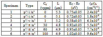
Details of the aSi:H samples used in the present work are summarised in Table 1. All specimens were deposited by plasma enhanced chemical vapour decomposition (PECVD) of silane gas onto glass substrates held at a temperature of about 290℃. The PECVD reactor conditions used during capacitively-coupled deposition were: RF power = 8 W at 40 MHz; partial chamber pressure = 150 mtorr; gas flow rate = 8 sccm. Systematic n-type and p-type doping of the a-Si:H films was respectively achieved through the controlled addition of phosphine or diborane in precisely determined volume parts per million (vppm) amounts during the PECVD growth process. Sample growth rates were typically about 1 Ǻs-1 and the films were generally sandwiched between 300 Ǻ thick heavily doped p+ and n+ layers to form diode junction structures (p+/ i /n+ for undoped films, p+/ ν /n+ for n-type films and p+/ π /n+ for p-type films). The film thicknesses (L) were sufficiently large (≈ 5 µm) to ensure that the measured (µτ)h values were representative of the true bulk magnitude and not influenced by contact complications[20].
Charge collection measurements were performed using a standard timeofflight (TOF) arrangement[1,2,21] with the diode devices subjected to a pulsed reverse voltage bias (Vr). Excess hole carriers were then generated in the vicinity of the n+ layer using a 5 ns dye laser operating at a wavelength of 570 nm which was synchronised to fire a short time (~50 µs) following the application of Vr. Experiments were performed under small-signal conditions and the amount of collected charge was subsequently obtained by numerical integration of the resulting transient photocurrents. A standard Hecht analysis[1] finally allowed the mobilitylifetime products of the hole carriers to be determined. Data for (µτ)h was recorded between temperatures (T) of 260 K and 425 K by mounting the samples in an evacuated cryostat. The location of the Fermi energy (EF) relative to the conduction band edge (EC) was estimated from the activation energy of dark conductivity measurements performed on the i, ν and π diode layers which were rendered devoid of the p+ and n+ layers by shielding selected substrates during the PECVD process.
Table 1. Specimens used for hole capture crosssection measurements
     

3. Results and Discussion

Examples of charge collection data are given in Figure 1 which shows how the amount of collected hole charge (Q) approaches a limiting saturated magnitude (Q0) as the reverse diode potential Vr is progressively increased. Under small-signal conditions Q0 was typically restricted to less than 10 pC.
The solid curves in Figure 1 represent the optimum fit of the data to the Hecht formula[1] which allows (µτ)h to be extracted according to:
(1)
The application of Equation 1 to the charge collection data yielded the (µτ)h values given in Table 1 at T =295 K where the underlying uncertainty is typically ± 10% and is mainly attributable to the associated error in the measurement of L (±0.2 µm).
It is initially informative to consider how these deduced (µτ)h values depend upon the associated values for EC EF. Dangling bonds may exist in three distinct charge states according to electron occupancy: unoccupied (D+); singly occupied (D0) or doubly occupied (D-). Hole capture by D+ states is consequently considered to be negligible, whereas the negative charge of the D centre is expected to render hole trapping into this state (h→D) more efficient than trapping into the neutral D0 state (h→D0). The variation of (µτ)h with Fermi energy may thus be explained qualitatively by the progressive decrease in the density of neutral (D0) DB states, and an accompanying increase in charged (D) DB states, as EF moves towards shallower energies in the band gap[17]. The relative rate of capture between these competing processes may be quantified by the ratio σh-h0 of the associated capture crosssections, and this dictates how rapidly (µτ)h varies with EC EF. By fitting the (µτ)h data in Table 1 to the occupation statistics for the D0 and D states it is therefore possible to determine σh-h0 and specify which trapping process (h→D or h→D0) will be dominant for a particular Fermi energy position. Experimentally, the desired change in EF induced by doping is also accompanied by an unavoidable increase in the DB density (NDB(D)) for doped a-Si:H films according to the well-established relationship[1]:
(2)
In Equation 2, ND is a proportionality constant (~ 3x1019 cm-3), and Cg is the concentration of dopant that is present in the gas-phase during film deposition. The dependence of NDB(D) upon Cg must therefore be taken into account before the variation of (µτ)h with EF may be correctly attributed to DB occupation statistics alone. Since (µτ)h ∝ NDB-1 this may conveniently be achieved by scaling the (µτ)h values in the doped specimens by a factor NDB(D) / NDB(U), where NDB(U) is the reference DB density in undoped material.
The expression used to quantitatively fit the variation of (µτ)h with EF is similar to that derived in the equivalent electron work[19] and for ballistic hole capture is given by:
(3)
In Equation 3 Vh and µv are the thermal velocity and free mobility values for holes at the valence band edge EV, and P0 and P are respectively the relative densities of D0 and D- centres for a given EC - EF. The detailed calculation of P0 and P- involves the numerical integration of an assumed DB DOS energy distribution throughout the a-Si:H band gap using the probability functions[22] that a DB contains either one (D0) or two (D-) electrons. For a-Si:H two distinctive types of DB DOS are considered where in both cases the total defect density may depend upon doping according to Equation 2: (i) a fixed DB DOS whose energy profile remains invariant with growth conditions and EF; (ii) a DB DOS whose energy profile is dictated by thermal equilibration processes during growth and is consequently sensitive to EF (so called defect-pool model[2,23]). Each of these possible DB DOS models are therefore used in Equation 3 and the parameters that are returned are compared.
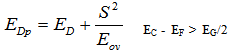
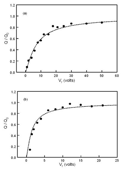
Figure 1. Charge collection data plotted as Q / Q0 against the applied reverse bias Vr at T = 295 K. The dashed lines represent the optimum fit of Equation1 to the data and yield (a) specimen 1: (µτ)h = 2.4x10⁻⁸ cm2V-1 (b) specimen 6: (µτ)h = 9.6x10⁻⁸ cm2V-1

3.1. Fixed DB DOS Analysis

For consistency with the previous electron work[19] both the D0 and D- states were initially assumed to have a Gaussian energy distribution with standard deviations S = 0.10 eV. The mean energy of the D0 state (ED) is located at EC - ED = 1.10 eV so that with a positive correlation energy U = 0.40 eV the D- state is located 0.70 eV below EC. Adopting these fixed DB DOS values the ensuing variation of P0 and P- upon the Fermi energy position is depicted in Figure 2 for T = 295 K. For completeness the relative density P+ of the D+ DB states is also plotted in Figure 2 since for all Fermi energy locations P0 + P- + P+ = 1.
By constraining the DB DOS the only quantity which may be adjusted in Equation 3 to fit the dependence of the experimental data upon EF is the magnitude of σh-h0. An example of the fitting procedure is shown in Figure 3, where the plotted (µτ)h points for the doped specimens have been adjusted by the scaling requirement described above to account for the incurred doping enhancement of NDB according to Equation 2. The value of the scaling factor clearly depends upon knowledge of NDB(U) for the undoped p+/ i /n+ specimens and for the data plotted in Figure 3 corrections have been applied for NDB(U) = 1.2x1016 cm-3. The effect of the selected NDB(U) magnitude upon the DB parameters that are returned by the analysis is discussed later.
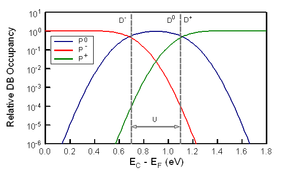
Figure 2. Variation of the occupation densities P0, P- and P+ for the D0, D- and D+ DB states with EC - EF. The DB DOS parameters used are fixed with EC - ED = 1.10 eV, S = 0.10 eV and U = 0.40 eV. The mean energies of the D0, D+ and D- states are indicated for reference
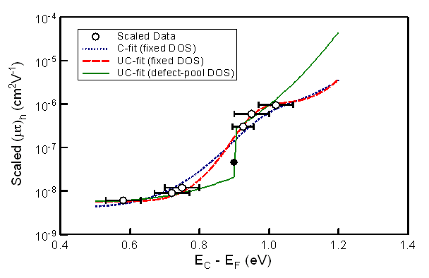
Figure 3. Experimental variation of scaled (µτ)h data at 295 K with EC - EF. The dashed curves show the best fits using the fixed DB DOS model: C – constrained (σh-h0 = 190); UC - unconstrained (EC-ED = 1.14 eV, S = 0.05 eV, U = 0.36 eV, σh-h0 = 182). The solid curve shows the best UC-fit using the defect-pool DB DOS model with Eov = 45 meV (EC - ED = 1.13 eV, S = 0.13 eV, U = 0.36 eV, σh-h0 = 9). Compensated data (•) taken from[25]
With the above NDB scaling correction applied (µτ)h is observed to increase by a factor of over 100 as EF is lowered from 0.55 eV to 1.05 eV below EC. For the limited range of accessible EC EF values the best fit to the data using Equation 3 is then obtained for σh-h0 = 190 as shown in Figure 3. An order of magnitude increase or decrease from this value is incapable of generating the observed dynamic range of (µτ)h, and furthermore is inconsistent with the detailed shape of the experimental data, particularly for larger values of EC - EF, where the densities of the D0 and D states begin to diverge. Conversely, it is seen in Figure 2 that for EC EF ≤ 0.7 eV P- ≥ P0 and the variation of (µτ)h with EF in this region is less sensitive to the magnitude of σh-h0. The fitting procedure would therefore benefit by extending the results towards larger values of EC EF but this unfortunately proves difficult in practice owing to the associated increase in dark ptype conduction which ultimately invalidates the charge collection technique employed.
Although the fitting procedure illustrated in Figure 3 would appear to suggest that the capture of holes is consistent with the DB DOS parameters (EC - ED, S and U) deduced in the previous electron work[19] it is instructive to consider whether alternative DOS parameter sets may also provide an acceptable fit, and how sensitive the parameters may be to the NDB(U) magnitude employed in Equation 3. An example of an alternative fit is included in Figure 3 where again NDB(U) = 1.2x1016 cm-3, but where EC - ED, S, U and σh-h0 are now all unconstrained to provide an optimum fit. The parameters returned under these circumstances are surprisingly close to the previously assumed DB DOS values with a similarly large σh-h0 ratio. By investigating the sensitivity of the DB DOS parameters over a typical range of DB densities in undoped a-Si:H[1-3] (3x1015 cm-3 < NDB(U) < 3x1016 cm-3) it is found that in all cases the observed rapid increase in (µτ)h as EF moves through the D- states towards the D0 states requires that: (a) the D0 state is located below mid-gap (1.09 eV < EC-ED < 1.16 eV); (b) the D0 and D- states are energetically well-defined (0.03 eV < S < 0.10 eV); (c) the D0 and D- states are energetically distinct (0.33 eV < U < 0.42 eV); These DOS parameters are generally comparable with those reported in independent studies[2,5] and are accompanied by large ratios for the capture cross-sections where 170 < σh-h0 < 240.
For the minimum deduced σh-h0 it is noted that the h→D0 and h→D capture rates are expected to become comparable when EC EF ≥ 0.97eV. Except for the most heavily doped ptype films, the capture of holes by DBs is therefore dominated by D as opposed to D0 states. The apparently large σh-h0 ratios that are returned from consideration of the occupation statistics for the D0 and D- states are not inconsistent with independent estimates in the literature where it is reported that 1 ≤ σh-h0 ≤ 1000[1-16]. Whilst a greater cross-section for the capture of holes into the charged D- centre is certainly anticipated on physical grounds, it is expected that the effect of the Coulomb potential will be diluted by the background disorder potential in a-Si:H with the consequence that the limiting magnitude of σh-h0 → 1[1, 24]. Under these limiting circumstances, however, (µτ)h would be predicted to decrease with EC - EF due to the associated increase in NDB(D). Such a decrease is not evident for the raw (un-scaled) (µτ)h data in Table 1 which is still found to require a minimum value of σh-h0 ~ 17 when fitted by Equation 3 under unconstrained fixed DB DOS conditions.

3.2. Defect-Pool DB DOS Analysis

To perform an equivalent analysis using the defect-pool DOS model it is now necessary to allow the mean energy of the D0 state to shift relative to ED in the fixed DOS situation depending upon whether the material is n-type or p-type in nature so that[2]:
(4a)
(4b)
In Equation 4, the band-gap EG = EC - EV, and Eov is the characteristic width of the valence band tail-states which is normally assumed to follow an exponential distribution of the form N(E) ∝ exp((E – EV)/Eov)[1-3]. Taking EG = 1.8eV for the present samples, Equation 4a is then applicable to specimens 1–3 in Table 1 while Equation 4b applies to specimens 4 -6.
Fitting Equation 3 to the (µτ)h data in Figure 3 now involves and additional independent variable Eov within the defect-pool framework, however, and in practice it was found that the minimisation approach used(Levenberg-Marquardt) was highly sensitive to local minima. To assist with the identification of true minima across the global parameter space unconstrained fitting was thus performed by assuming fixed values for Eov. An example of the fitting procedure is shown in Figure 3 where Eov = 45meV has been used in Equation 4 and again NDB(U) = 1.2x1016 cm-3. The quality of the defect-pool fits were generally found to be comparable to those generated using the (unconstrained) fixed DOS assumption although it is evident in Figure 3 that the critical fitting region occurs around EC - EF ~ EG/2 where no experimental data is presently available.
The DB DOS parameters that are found using the defect-pool model were investigated across a range of Eov and NDB(U) and are summarised in Figure 4 where the plotted points and associated error bars represent the mean and standard deviation of the fitted DB DOS parameters that are returned for a given Eov as NDB(U) is reduced in 10% steps from 3x1016 cm-3 to 3x1015 cm-3. A comparison with the equivalent parameter sets found using the fixed DB DOS analysis reveals that there is very close agreement for the values of EC - ED, S and U across the entire Eov range. By contrast there is a distinct reduction in the σh-h0 magnitude by a factor of about x20 (5 < σh-h0 < 10). The much smaller capture cross-section ratio is a direct consequence of the defect-pool shift in the D0 energy whereby there is a sudden predominance of D0 centres in p-type specimens as the D0 state is shifted upwards relative to n-type specimens (Equation 4). This is in contrast to the fixed DB DOS situation where there is a much more gradual conversion of D- to D0 states as EF moves down through the correlation energy U towards EV. The ensuing effect upon P0 and P- then demands that σh-h0 is much larger in the fixed DB DOS situation to account for the dynamic range of (µτ)h as EF is varied. Whilst the smaller σh-h0 ratios that are inferred by the defect-pool analysis appear to be physically more reasonable for carrier capture by charged defects in amorphous materials, additional (µτ)h data in the region of EC - EF ~ EG/2 is required to fully resolve whether this model is also quantitatively acceptable for any EF location. It is interesting to note, however, that (µτ)h data obtained using identical experimental methods on compensated a-Si:H films[25] would appear to provide additional support for the defect-pool DOS provided EC – EF = EG/2 as observed in Figure 3.
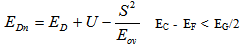
Figure 4. The dependence of the fitted defect-pool DB DOS parameters upon the assumed value for Eov. (a) EC - ED (b) S (c) U (d) σh-h0

3.3. Temperature Dependence of Capture Cross-Sections

Additional insight into hole capture by the D0 and D- states may be provided by examining the underlying temperature dependence of the cross-sections (σh(T)). From the electron work[18,19] the capture of electrons (e) by DBs was found to proceed by physically distinct mechanisms with the e→D0 capture being identified as a strong multiphonon emission process, whereas the e→D+ capture was interpreted as being Coulombic in nature. To experimentally investigate σh(T) it is noted from Equation 3 that as P0 and P- are only weakly dependent upon temperature through statistical shifts in EF[1], the main temperature influences are likely to arise from µv(T) and (µτ)h(T) so that σh(T) may be expressed as:
(5)
The temperature dependence of µv(T) is expected to be weak on theoretical grounds with µv(T) ∝ T[1,2] and values of γ ≤ 1.0 have been inferred from the analysis of µv(T) using hole TOF data[26]. The temperature dependence for the hole capture cross-sections may therefore be experimentally explored by measuring (µτ)h as a function of temperature. Data obtained for two representative samples are presented in Figure 5 where µv has initially been assumed to be temperature independent (γ = 0) so that σh(T) ∝ (µτ)h(T)-1. Based upon the preceding analysis the specimen 1 data is expected to be dominated by h→D- capture events and should thus reflect the thermal signature for σh-(T), whereas the specimen 6 data is mainly due to h→D0 events and should correspond to σh0(T). In both cases a similar temperature dependence of the form σh(T) ∝ Tβ is obtained where β ≈ 2.0 ± 0.2. The actual β values that are returned will clearly depend upon the value that is assumed for γ, however, so that β ≈ 2 + γ from Equation 5.
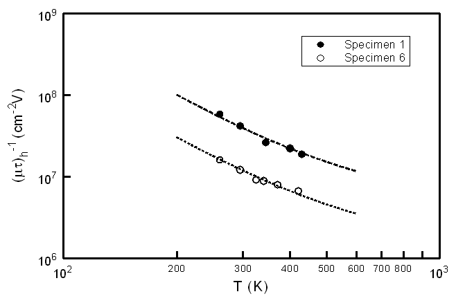
Figure 5. Double logarithmic plots of (µτ)h-1 against temperature for specimen 1 and specimen 6. The dashed lines represent the best fit of Equation 6 to the data for which Eov = 45 meV
The similar type of temperature behaviour that is obtained for σh0(T) and σh-(T) is unexpected for capture into defect centres possessing different charge states. Although a T-2 dependence is predicted from simple considerations of capture at a Coulomb potential well[27], this is generally weaker than the β values suggested from Figure 5 unless γ = 0. However, since the crystalline theory describing Coulomb capture is based upon a cascade of transitions down the boundstates of the Coulomb potential, such a model may be inappropriate for amorphous solids where the disorder potential may exceed the Coulomb potential of the charged centre at distances of the order of the capture radii. For the neutral capture process the situation is also confusing since neutral capture in crystalline solids (and crystalline silicon in particular) is generally observed to be temperature independent[28] or to increase with temperature[29].
Similar σ(T) investigations by Street for both electrons and holes also reveal power law capture behaviour of the form σ ∝ T-β into both neutral and charged danglingbond centres in aSi:H[24]. To explain this behaviour, a model that acknowledges the increasing importance of the tunnelling of trapped bandtail charge to danglingbond defects at lower temperatures was proposed. The introduction of tail-state tunnelling is demonstrated to enhance the effective cross-section magnitudes for the direct DB capture of holes at the valence band edge by a (temperature dependent) factor (1 + Q(T)). For an exponential valence bandtail the enhancement factor Q(T) may be approximated as follows (where kB = Boltzmann’s constant)[24]:
(6)
Over a restricted temperature range Q(T) is therefore capable of accounting for the behaviour displayed in Figure 5 as illustrated by the dashed curves which represent the optimum fit across both data sets using Eov as a common fitting parameter. For the temperature range that is accessible in the present work, values of Eov between 45 meV and 103 meV are found as the assumed value for γ is increased from 0 to 1.0. Valence band tail widths for a-Si:H which is lightly boron doped are reported to lie towards the lower end of this Eov range[3] which suggests that µv in Equation 5 is indeed very weakly temperature dependent. Tunnelling transitions between localised valence bandtail states anddanglingbond defects may therefore account for the observed σh0(T) and σh-(T) behaviour in aSi:H, assuming that the corresponding cross-sections for direct hole capture are essentially temperature independent. As the absolute magnitude of Q(T) is estimated to be larger by a factor of at least 3 for charged DBs compared to neutral DBs[24] the underlying cross-section ratio for direct hole capture may actually be as low as ~ 2 ↔ 3 based upon the data in Figure 4d. The apparent absence of similar tunnelling-enhanced capture of electrons by DBs above room temperature presumably reflects the much narrower distribution of conduction band tailstates[3].

3.4. Capture Cross-Section Radii

The absolute magnitude of the (µτ)h values that are generated by Equation 3 is determined by a pre-factor quantity µv / (NDB(U)σh0Vh) which is independent of EF and may therefore be used to provide an estimate for σh0, and subsequently σh- using the σh-h0 ratio. For the parameter set returned in Figure 4 it is found that µv / (NDB(U)σh0Vh) = 3.8 ± 0.6 x10⁻⁸ cm2V-1. Taking literature values for Vh = 107 cms-1 and 1 cm2V-1s-1 < µv < 10 cm2V-1s-1[1-3, 25] it is then found that 8x10-17 cm-2 < σh0 < 1x10-14 cm-2 for 3x1015 cm-3 < NDB(U) < 3x1016 cm-3. The capture radius for σh0 is thus estimated to lie between 0.5 Ǻ and 5.6 Ǻ, and with σh-h0 ≤ 10 the corresponding capture radius associated with σh- has a minimum value of 1.6 Ǻ. These capture radii accordingly fulfil the criterion for the use of a ballistic capture pre-factor in Equation 3 since the scattering length is estimated to be greater at around 2 Ǻ for the lower µv limit[24].

4. Conclusions

The variation of experimental (µτ)h data with EF in a-Si:H is qualitatively consistent with a hole capture rate which is greater for charged compared to neutral DB states. The relative occupation density of D0 to D- states with EF may consequently be used to estimate the underlying magnitude for σh-h0. Quantitative fitting of the (µτ)h data using alternative DB DOS models reveals that the capture cross-section ratio σh-h0 may vary from greater than 170 (fixed DOS) to less than 10 (defect-pool DOS). Whilst the smaller σh-h0 values returned by the defect-pool DOS appear to be more physically plausible for a-Si:H there is presently insufficient experimental data to discount the fixed DOS possibility on quantitative model fitting evidence alone. The temperature dependence of the hole capture cross-sections suggests that the capture of holes by DBs is enhanced by valence band-tail tunnelling transitions at room temperature in a-Si:H.

References

[1]  R. A. Street, Hydrogenated Amorphous Silicon, Cambridge Solid State Science Series, Cambridge, United Kingdom: Cambridge University Press, 1991.
[2]  K. Morigaki, Physics of Amorphous Semiconductors, London, United Kingdom: Imperial College Press, 1999.
[3]  Properties of Amorphous Silicon and its Alloys, EMIS DataReviews Series No.19, ed. T. Searle, London, United Kingdom: INSPEC, IEE, 1998.
[4]  Li, T. A., McIntosh, K. R. and Cuevas, A., 2008, Limitations of a simplified dangling bond recombination model for a-Si:H, J. Appl. Phys, 104(11), 113718 1-6.
[5]  Hubin, J., Shah, A. V., Sauvain, E. and Popoz, P., 1995, Consistency between experimental data for ambipolar diffusion length and for photoconductivity when incorporated into the standard defect model for a‐Si:H, J. Appl. Phys, 78(10), 6050-6059.
[6]  Asensi, J. M., Merten, J., Voz, C. and Andreu, J., 1999, Analysis of the role of mobility-lifetime products in the performance of amorphous silicon p-i-n solar cells, J. Appl. Phys, 85(5), 2939-2951.
[7]  Beck, N., Wyrsch, N., Hof, C. and Shah, A., 1996, Mobility lifetime product – a tool for correlating a-Si:H film properties and solar cell performances, J. Appl. Phys, 79(12), 9361-9368.
[8]  Prentice, J. S. C., 2000, Effect of gap-state parameters in intrinsic a-Si:H, J. Non-Cryst. Sol, 278, 164-169.
[9]  Klimovsky, E., Rath, J. K., Schropp R. E. I. and Rubinelli, F. A., 2002, Errors in a-Si:H-based solar cell modelling when dangling bonds are approximated by decoupled states, Thin Solid Films, 422(1-2), 211-219.
[10]  Kuznetsov, S. V., 2003, Independence of photoconductivity of p-type a-Si:H films on doping level and defect concentration, J. Non-Cryst. Sol, 316(2-3), 217-227.
[11]  Morgado, E., 2004, Influence of light-soaking and annealing on electron and hole mobility-lifetime products in a-Si:H, J. Non-Cryst. Sol, 338-340, 386-389.
[12]  Meaudre, R. and Meaudre, M., 2004, Method for the determination of the capture cross-sections of electrons from space-charge-limited conduction in the dark and under illumination in amorphous semiconductors, Appl. Phys. Lett, 85(2), 245-247.
[13]  Olibet, S., Vallat-Sauvain, E. and Ballif, C., 2007, Model for a-Si:H/c-Si interface recombination based upon the amphoteric nature of silicon dangling bonds, Phys. Rev. B, 76(3), 035326 1-14.
[14]  Wolf, S., Olibet, S. and Ballif, C., 2008,Stretched-exponential a-Si:H/c-Si interface recombination decay, Appl. Phys. Lett, 93(3), 032101 1-3.
[15]  Plagwitz, H., Terheiden, B. and Brendel, R., 2008, Staebler-Wronski-like formation of defects at the amorphous- silicon-crystalline silicon interface during illumination, J. Appl. Phys, 103(9), 094506 1-4.
[16]  Gradisnik V. and Linic, A., 2013, Defects in p-i-n a-Si:H photodiode i-layer, J. Non-Cryst. Sol, 363, 193-198.
[17]  Spear, W. E., Steemers, H. L. LeComber, P. G. and Gibson, R. A., 1984, Majority and minority carrier lifetimes in doped a-Si:H junctions and the energy of the dangling-bond state, Phil. Mag. B, 50(3), L33L40.
[18]  Spear, W. E., Hourd, A. C. and Kinmond, S., 1985, The temperature dependence of the D0 and D+ capture cross-section in a-Si, J. NonCryst. Sol, 77-78(1), 607-610.
[19]  LeComber, P. G. and Spear, W. E., 1986, The energy of the dangling-bond sates in a-Si, Phil. Mag. B, 53(1), LlL7.
[20]  Steemers, H. L., Spear, W. E. and LeComber, P. G., 1983, Thickness dependence of excess carrier lifetime and mobility in a-Si:H junctions, Phil. Mag. B, 47(5), L83-L88.
[21]  Spear, W. E. and Steemers, H. L., 1983, The interpretation of drift mobility experiments on amorphous silicon, Phil. Mag. B, 47(5), L77-L82.
[22]  Schweitzer, L., Grunewald, M. and Dersch, H., 1981, Influence of correlation effects on the electronic properties of amorphous silicon, J. de Physique, 42(10), 827-830.
[23]  Winer, K., 1989, Chemical-equilibrium description of the gap-state distribution in a-Si:H, Phys. Rev. Lett, 63(14), 1487-1490.
[24]  Street, R. A., 1984, Disorder effects on deep trapping in amorphous semiconductors, Phil. Mag. B, 49(1), L15L20.
[25]  Goldie, D. M., Spear, W. E. and Liu, E. Z., 1990, Electron and hole transport in compensated amorphous silicon, Phil. Mag. B, 62(5), 509-525
[26]  Goldie, D. M. and Spear, W. E., 1988, The extended-state hole mobility in amorphous silicon, Phil. Mag. Lett, 57(2), 135-141.
[27]  Lax, M., 1960, Cascade capture of electrons in solids, Phys. Rev, 119(5), 1502-1523.
[28]  Brotherton, S. D. and Bradley, P., 1982, Defect production and lifetime control in electron and γ‐irradiated silicon, J. Appl. Phys, 53(8), 5720-5732.
[29]  Henry, C. H. and Lang, D. V., 1977, Nonradiative capture and recombination by multiphonon emission in GaAs and GaP, Phys. Rev. B, 15(2), 989-1016.