-
Paper Information
- Next Paper
- Previous Paper
- Paper Submission
-
Journal Information
- About This Journal
- Editorial Board
- Current Issue
- Archive
- Author Guidelines
- Contact Us
American Journal of Materials Science
p-ISSN: 2162-9382 e-ISSN: 2162-8424
2013; 3(2): 29-35
doi:10.5923/j.materials.20130302.02
Nano-Sized Inclusions Influence on Semiconducting Material: Proton-Irradiated Silicon
 Abstract
 Reference
 Full-Text PDF
 Full-text HTML
Temur Pagava, Levan Chkhartishvili
Department of Physics, Georgian Technical University, Tbilisi, 0175, Georgia
Correspondence to: Levan Chkhartishvili, Department of Physics, Georgian Technical University, Tbilisi, 0175, Georgia.
| Email: |  |
Copyright © 2012 Scientific & Academic Publishing. All Rights Reserved.
Formation of the nanoscale inclusions is an effective way to control the properties of semiconductors, when required characteristics of the material cannot be achieved by the standard method of doping. Typically, these inclusions are “dielectric”, i.e. possess lower conductivity than the semiconducting matrix. Formation of the “metallic” inclusions, i.e. regions with higher conductivity than that of matrix, opens completely new perspectives to control material properties. There is demonstrated that the “metallic” clusters of radiation defects generated in single-crystalline silicon by the high-energy proton irradiated may be transformed into the “dielectric” ones and vice versa through a certain cycle of isochronous annealing.
Keywords: Nano-Sized Inclusions In Semiconductor, Electro-Physical Properties, Silicon
Cite this paper: Temur Pagava, Levan Chkhartishvili, Nano-Sized Inclusions Influence on Semiconducting Material: Proton-Irradiated Silicon, American Journal of Materials Science, Vol. 3 No. 2, 2013, pp. 29-35. doi: 10.5923/j.materials.20130302.02.
1. Introduction
- Traditionally, tuning of the properties of semiconductor materials is based on their doping with chemical elements creating the electronic levels within the band gap. However, in some cases this method cannot be realized due to the absence of impurities with suitable levels, low solubility of an impurity in semiconducting substance, high concentration of electrically active structural defects (both intrinsic and generated in the process of doping), etc. In this regard, it has been actively developed an alternative approach to the creation some kind nanoscale inclusions in semiconducting matrices. Physical mechanisms and methods of formation of the nano-sized atomic clusters in semiconductors have been considered in[1].In semiconductors, the stable complexes of various types can be formed by elastic, electrostatic or chemical interactions between host atoms, dopant and residual impurities, as well as intrinsic point defects. Effective technologies of the formation of these inclusions are: combination of different types of radiation and heat treatments, laser and rapid thermal annealing, plasma-chemical etching, complex doping, gettering the rapidly diffusing impurities and defects, ion implantation, doping with isovalent impurities, chemical heat treatment, passivation of electrically-active and recombination centers, etc.Frequently, nanoscale inclusions are formed by the decomposition of supersaturated solid solutions both directly, when they are grown in the cooling process, and during the subsequent heat or other external treatments of the material that contains dopant and residual impurities or vacancies and interstitials in concentrations above their solubility limits, e.g., clusters of intrinsic interstitial atoms can be formed in the supersaturated solid solution based on crystalline silicon (because of the rather large interstitials characteristic for this lattice the corresponding elastic strain energy is too small). A typical example of the formation of supersaturated solid solutions of the residual impurities is oxygen-rich single-crystalline silicon grown by the Czochralski method.It should be noted that typically the volume-share of nanoscale inclusions in the semiconductor matrix is less than a few percents. To obtain materials with such kind inclusions in a significant volume-share, one should use special techniques such as direct deposition of semiconductor nano-clusters on substrates or initial-stage crystallization inside hydrogenated amorphous semiconductors resulting in composites of large number of nano-crystals and amorphous matrix. Another example of a nano-cluster material is porous silicon, in which the pores average size is a few nanometers.In view of the small sizes of inclusions, the corresponding electron wave function may be confined by a potential barrier. Thus, nano-inclusions can create the local levels within the band gap, similar to the impurities levels, and thus have a significant impact on the fundamental semiconducting properties being the effective centres of radiative and non-radiative recombination, and determining to a large extent the degree of compensation, concentration and scattering of the charge carriers, material photosensitivity, etc. All these allow the elaboration of unique device structures widely used in electronics, e.g. advanced semiconductor lasers[2].From the point of view of electro-physical properties, nano-inclusions may be “dielectric” or “metallic” depending on their conductivity, which can be much less or much more than that of the semiconducting matrix. In this regard, for silicon, the basic material of modern electronics, the situation is as following. Semi-insulating and true-dielectric inclusions can be obtained, e.g. applying material passivation by acceptors diffusion in electron-conductivity regions in the process of formation of two-dimensional microcavities embedded in the plane ultra-narrow quantum wells[3] or local oxidation forming silicon dioxide when manufacturing microring resonators[4], etc. In addition, porous silicon is widely used in photonics[5], electrical[6] and solar[7] batteries, etc. because the pores act as perfect (with zero conductivity) dielectric inclusions.The true metallic nano-clusters embedded in a semiconducting matrix usually contain a sufficiently large number of atoms to affect the material properties by the different doping mechanism[8]. If at the metal–semiconductor interfaces Schottky barriers are formed the Fermi level is placed near the middle of the band gap. Therefore, both in n- and p-type semiconductor matrices the space-charge layers adjacent nano-contacts have to appear. These layers are essentially non-transparent to the charge carriers. So, true-metallic inclusions effectively act as “dielectric” ones.Recently, in silicon samples irradiated with high-energy protons and heat-treated in a certain way, we observed[9, 10] a sharp increase in effective Hall mobility of charge carriers within the temperature-range of phonon-scattering. Such high values indicate the creation of high-conductivity, i.e. “metallic”, inclusions with Ohmic contacts at the interfaces with the semiconductor matrix[11]. Apparently, in silicon these inclusions are nano-clusters of interstitial atoms, which in this material can be intensively formed by irradiation with light ions and heat treatments[12, 13].This paper aims to examine the feasibility of formation in silicon both “dielectric” and “metallic” nanoscale inclusions, as well as their mutual transformation through a combination of high-energy proton-irradiation and isochronous annealing (IA) of corresponding radiation defects (RD). Our results may give impact to the development of semiconducting materials technology of new type.
2. Experimental and Results
- The test specimens were the single crystals of n-Si of sizes 1 mm × 3 mm × 10 mm doped with phosphorus P to the concentration of 6 • 1013 cm–3. They were irradiated by the 25 MeV energy protons at ambient temperature 300 K. The radiation dose was 8 • 1012 cm–2. The irradiated crystals were subjected to IA in the temperature range 80 – 600 С with step of 10 С for 10 min.We have studied changes in the character of electrons Hall-concentration nH, Hall-mobility μH and material conductivity σ dependences on temperature T in specimens treated at annealing temperatures Tann from the range 80 – 600 С. Hall-measurements were performed not only in the dark, but also under the illumination (photo-Hall-effect). IR illumination was selective monochromatic with photon energies of 0.17 and 0.44 eV which correspond, respectively, the ionization energies of A-and E-centers – vacancy complexes with oxygen O and phosphorus P, the dominant electron-levels in irradiated silicon. The level of charge carriers injection estimated from their concentration temperature-dependences obtained both in the dark and under IR illumination did not exceed ~ 5 %. Ohmic contacts needed in the Hall-measurements were made by rubbing aluminum Al on the samples surfaces. Characteristics nH – T, μH – T and σ – T were mapped from the nitrogen boiling point up to room temperature, 77 – 300 K, with relative errors less than ∼ 10 %. The specimen temperatures during Hall measurements and IA process were monitored, respectively, by copper–constantan and chromel–alumel thermocouples. The obtained curves are shown in Figs. 1, 2 and 3.The curves were treated as follows. Ionization energy Ei of the i-type levels are determined by the slope of the nH – T characteristics. Concentrations of various RDs after each IA process are calculated based on nH – T and nH – Tann stepwise dependences within the temperature ranges 77 – 300 K and 80 – 600 С, respectively.
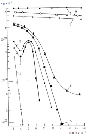 | Figure 1. Dependence of electron Hall concentration on reciprocal temperature in n-Si crystals irradiated with protons: 1 – before irradiation, 2 – after irradiation, after annealing at 3 –110 and 4 – 160 С, 5 – under IR illumination with photon energy of 0.44 eV after annealing at 110 С, 6 – under IR illumination with photon energy of 0.17 eV after annealing at 160 С, after annealing at 7 – 400 and 8 – 550 С |
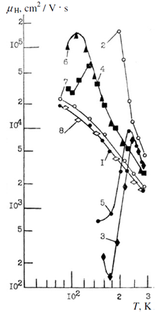 | Figure 2. Dependence of electron Hall mobility on temperature in n-Si crystals irradiated with protons: 1 – before irradiation, 2 – after irradiation, after annealing at 3 –110 and 4 – 160 С, 5 – under IR illumination with photon energy of 0.44 eV after annealing at 110 С, 6 – under IR illumination with photon energy of 0.17 eV after annealing at 160 С, after annealing at 7 – 400 and 8 – 550 С |
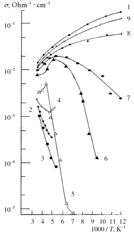 | Figure 3. Dependence of conductivity on reciprocal temperature in n-Si crystals irradiated with protons: 1 – before irradiation, 2 – after irradiation, after annealing at 3 – 80, 4 – 90, 5 – 110, 6 – 120, 7 – 290, 8 – 350 and 9 – 550 С |
3. Discussion
- The obtained results have been analyzed based on the following data available on RDs in silicon.In crystals irradiated by particles with relatively low energy, it can be formed a large diversity of point defects. Dominant ones are complexes of vacancies with donor, usually phosphorus P: V + P, i.e. E-center; acceptors, usually boron B: V + B; residual impurities, usually oxygen O: V + O, i.e. A-center, and carbon C; divacancy V2, as well as multi-complex point RDs of VmOn-type, m, n = 1, 2, 3, … , determining the basic semiconducting properties of the irradiated silicon up to annealing temperature of 600 С[14-16].However, an irradiation with high-energy (> 10 MeV) particles forms complex structural damages, so-called disordered regions (DRs), which according to the model[17] are non-transparent for charge carriers, i.e. act as “dielectric” inclusions.A review on the effects of radiation-induced displacement damage in semiconductor materials and devices with emphasis placed on effects in technologically important bulk silicon devices was provided in[18]. Energetic heavy particles incident on a solid lose their energy to the production of displaced atoms as they travel through the material. In particular, incident protons with energies > 10 MeV produce a mixture of isolated point and clustered defects. The primary point defects initially created in lattice are the combinations of a vacancy and an adjacent interstitial – Frenkel pairs. When a number of Frenkel pairs are produced relatively close together they form a local region of disorder referred as a defect cluster. The mechanism involved is the initial transfer of a significant amount of energy from single incident proton to a single Si atom. The dislodged primary knock-on atom then displaces many other Si atoms locally, thereby creating a DR. Once defects are formed by incident radiation, those defects will reorder to form more stable configurations. Because the vacancy in silicon is an unstable defect and is quite mobile at room temperature, after vacancies are introduced they move through the lattice and form more stable defects such as vacancy–impurity complexes and divacancies or larger local groupings of vacancies. This is a reason why disordered nano-inclusions in irradiated silicon mainly consist of interstitial atoms and, in lesser extent, vacancy-complexes.In silicon crystals containing DRs, within the phonon-scattering temperature range there is observed the decrease in effective (measured) values of the charge carriers’ Hall mobility related to the reducing in the volume allowed for their movement[19]. DRs, if they are localized, are annealed at 200 – 260 С. But, at high irradiation doses, when amorphous layers are formed inside the crystal, the structure characteristic of crystalline silicon is restored only after annealing at 570 C[20]. In the samples irradiated with high-energy protons, after natural aging at ambient temperature 300 K for 30 days (or low-temperature, 90 C, annealing) one can observe the sharp reduction in the effective Hall mobility of electrons. We have attributed[9] this effect with screening the clusters of interstitial atoms by the negatively charged secondary RDs that are formed around these inclusions in the process of aging.Analyzing performed Hall-measurements, we tried to determine: (i) what defects are the sources of non-equilibrium vacancies generated in the process of IA; (ii) the type of RDs formed during quasi-chemical reactions between impurity atoms and non-equilibrium vacancies concentrated around “metallic” inclusions; (iii) what RDs are responsible for the screening the “metallic” inclusions and, correspondingly, the effective reduction of the effective mobility; and (iv) the dependence of the characteristic radius of “metallic” inclusions on the IA temperature and the temperature of their complete annealing.Curves 2 – 4 in Fig. 1 correspond to the depleted acceptor centers EC – 0.38 eV, i.e. divacancies. This means that all the free electrons are captured by the E-centers, divacancies and some unidentified defects with levels at EC – 0.54 eV and EC – 0.57 eV. As for the A-centers, they are in neutral state and, consequently, their concentration cannot be determined from nH – T curves. After a certain part of E-centers is annealed (Tann ≥ 100 С), A-centers became charged and one can track the changes in their concentration during IA.As can be seen from Fig. 2, immediately after exposure to the test crystals they provide the increased electron mobilities (Curve 2). After the annealing at 80 C, the electron mobility, as well as conductivity decrease slightly. but, they grow again after the annealing at 90 C (Fig. 3, Curves 3 and 4). The annealing at 110 C leads to the appearance the μH – T curve, in which the mobility values are reduced by almost an order of magnitude if compared to initial ones (Fig. 2, Curve 3). The annealing at 160 С increases mobility values, but they remain still less than in irradiated non-annealed specimen (Fig. 2, Curve 4).In[9, 10], the increasing in μH value immediately after irradiation by 25 MeV protons has been explained by the formation of “metallic” inclusions with Ohmic contacts at the boundaries with matrix. These inclusions are clusters of interstitial atoms creating in silicon elastic stresses and, consequently, reducing Tann for vacancy defects, such as tetravacancies V4, etc.[14]. It is known that even at Tann = 110 С the significant part of E-centers are annealed.Non-equilibrium vacancies that are the decay products of V4 and E-centers move toward to clusters of interstitials and participate in quasi-chemical reactions with impurity atoms. At the initial stages of the IA of E-centers, around clusters of interstitial atoms in addition to RDs with high thermal stability (e.g. A-centers) there are again generated E-centers. As a result, around these inclusions there are formed the negatively charged shells of secondary RDs (A- and E-centers, V2, etc.) non-transparent for the conduction electrons. They cause the observed decrease in μH value after annealing at 110 C (Fig. 2, Curve 3).It should be noted that A-centers formed around the clusters of interstitial atoms in the vicinity of minimum at 180 K are uncharged and, therefore, not in a position to cause a decrease in mobility. As for the formation of divacancies from the charged monovacancies, this process seems to be unlikely because strong electrostatic repulsion between reagents. It remains to think that E-centers are responsible for the reducing in the mobility at 180 K: at this temperature they are formed more efficiently than other RDs in result of the reaction between positively charged donors P+ and negatively charged vacancies V –.For the sources of non-equilibrium vacancies in process of the IA, apparently, serve also RDs of vacancy-type, which are undoubtedly presented in proton-irradiated silicon crystals. As noted[9], they play an important role in the formation of non-transparent for conduction electrons shells around the “metallic” inclusions.The occupancy k of the deep centers existing in the atmosphere around clusters of interstitial atoms is close to 1. The energy of interaction between these centers is E ≈ k E0, where E0 = e2 / ε d ≈ 0.5 eV (ε is the silicon dielectric constant and d and is the average distance between neighboring defects). As noted, a significant part of the E-centers are annealed by the heat treatment at 110 С. The concentrations of the electrons released during this process and charged A-centers will be 2-fold greater (depletion of A-centers corresponds the monotonic curve). The above mentioned electrostatic interaction between the negatively charged defects will change their energies of deionization. Apparently, when Ei ≥ 0.17 eV the excitation of electrons from the A-centers into the conduction band occurs at lowered temperatures than usually. Because of the electrostatic interaction into the conduction band electrons are transferred not only from A-centers, but also from some deeper levels. In addition, electrons are transferred from centers associated with complexes of interstitial and substituting carbon atoms CiCs with level at EC – 0.16 eV[21, 22]. As a result, the slope-angle of the corresponding nH – T curve increases and the electrons Hall concentration reaches its maximum at 200 K. After deionization of A-centers the electrostatic forces of interaction between the radiation-induced defects reduce.At 250 K, free electrons are trapped by the deep levels. In the conduction band, it remains electrons with the concentration of 4 • 1012 cm–3, which corresponds to A-centers charged during the annealing of E-centers at 110 С. With further increase in the measurement temperature the electron concentration increases monotonously. In case of absence the electrostatic interactions, this value would change so that the slope of the curve reveal the depletion of A-centers.The total concentration of A-centers is 2.5 • 1013 cm–3. Its increasing up to 3 • 1013 сm–3 in the irradiated crystal after annealing at 290 С is related to the additional formation of A-centers during the annealing of divacancies in the temperature range 225 – 290 C. At Tann = 300 С, it starts the annealing of A-centers[23] and they are fully annealed at Tann ≈ 400 С (Fig. 1, Curve 7).In the process of IA, a significant part of E-centers are annealed at 120 С, while the concentration of additionally created E-centers is negligible. Accordingly, the energy of the electrostatic interaction between the negatively charged defects decreases and the nH – T curve rises monotonously. Behavior of the nH – T characteristic cannot be changed even after annealing at higher temperatures (up to Tann = 600 С).In this case, after the annealing of E-centers in the defect-impurity atmosphere around the “metallic” inclusions the degree of screening of clusters of interstitial atoms decreases leading to an increase in the effective value of μH (Fig. 2, Curve 4).The observed oscillations of the electrons Hall mobility value at a given temperature can be explained by the changes in the degree of screening of clusters of interstitial atoms in the process of IA. Changes in concentrations and the charge states of the RDs which can influence the degree of screening of “metallic” inclusions affect the charge carriers’ mobility in silicon.Annealing of the E-centers increases the crystal conductivity allowing the Hall measurements below to the nitrogen boiling point. At ≤ 140 K, A-centers are completely charged. This would undoubtedly lead to an increase in the degree of screening the clusters of interstitials and thus decrease in μH, as it was observed experimentally. After the annealing of A-centers (at 350 С) decrease in the μH values in the vicinity of 77 K is not observed.After the annealing at 550 C, the temperature-dependence of the electron Hall mobility characteristic of initial crystal practically restores (and further does not change). At this temperature, clusters of interstitial atoms seem to be finally annealed (Fig. 2, Curve 8). Although, the concentration of electrons after the IA cycle is not completely restored (Fig. 1, Curve 8). This must be due to the formation of deep RDs in the process of crystals cooling after their annealing at 600 С.Suggested interpretation of the Hall measurements in the dark have been confirmed by experiments on the photo-Hall-effect. In the specimen annealed at 110 С, electrons photo-excited from the level of 0.44 eV in the conduction band increase the μH value in the minimum and at the same time slightly shifts its position to lower temperatures (Fig. 2, Curve 5). On the other hand, in the sample annealed at 160 С electrons photo-excited from the level of 0.17 eV increase the μH value in the maximum also shifting its position to lower temperatures (Fig. 2, curve 6). In general, from Fig. 2 one can see that the illumination affects the μH – T dependence not only at relatively low temperatures (~ 100 K), i.e. in the region of scattering by charged centers, but also at higher temperatures (≥ 180 K), when the phonon scattering mechanism is dominant.The increase of μH within the range of 140 – 230 K under the IR photo-excitation of electrons from the level EC – 0.44 eV is explained by the reduction in degree of screening of the atomic clusters and the corresponding increase in the volume-share of “metallic” inclusions. In the same temperature interval, E-centers segregated around the “metallic” inclusions are exhausted due to the influence of high temperature and electrostatic interaction between neighboring centers. When electrons are IR photo-excited from the EC – 0.17 eV level the similar effect is observed at ∼ 100 K and associated with the deionization of A-centers. Photo-excitation of electrons from the level EC – 0.44 eV into the conduction band leads to an increase in the effective Hall mobility of electrons in a broader temperature range than that from the level EC – 0.17 eV since E-centers, in contrast to the A-centers, are negatively charged over the entire interval of measurements.Thus, the results obtained by the photo-Hall-effect method once again confirm the above considerations that the screening of “metallic” inclusions, i.e. their transformation into quasi-dielectric ones, is mainly caused by the negatively charged A- and E-centers segregated in the shells of such inclusions.Based on changes in the value of the electron mobility at 300 K, we are able to trace the changes in the average radius R of the atomic clusters during the IA of irradiated n-Si crystals. This value can be estimated by the formula R = √3 f / 4 π N, where N is the concentration of atomic clusters, which in n-Si crystals irradiated with 25 MeV protons with the dose of 8 • 1012 cm–2 equals ~ 5 • 1013 cm–3[10]; and f is the inclusions volume-share calculated from the relation μeff = μH (1 + 3 f) / (1 – 6 f)[11]. Here μeff stands for the effective mobility of electrons in irradiated crystals, while μH is electron Hall mobility before irradiation. The obtained dependence R – Tann is shown in Fig. 4.
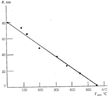 | Figure 4. Average radius of nano-sized atomic clusters in proton-irradiated n-Si crystals versus annealing temperature |
4. Conclusions
- We have shown that the high-energy proton irradiation in the n-Si crystals mainly forms relatively highly conducting inclusions with Ohmic contacts at the interface with the semiconductor matrix. It explains the observed increase in the effective electron Hall mobility. Such inclusions have to be clusters of interstitial atoms, which generate elastic stresses. In the process of isochronous annealing, dissociation products of the vacancy-type radiation defects – non-equilibrium vacancies move toward these inclusions. A certain portion of vacancies recombines with interstitial atoms. Others engaging in quasi-chemical reactions with impurity atoms around the clusters of interstitials create negatively charged and consequently non-transparent for conduction electrons shells containing A- and E-centers and other acceptors (creation of divacancies from pairs of negatively charged vacancies is unlikely because their electrostatic repulsion). These processes explain the decrease in the Hall mobility effective value. At high temperatures, 200 – 300 K, E-centers become responsible for the screening the “metallic” inclusions, while below 200 K – not only E-, but also A-centers.Clusters of interstitials finally are annealed at 550 С. As all the main secondary radiation defects (E-centers, divacancies and A-centers) and vacancy-type disordered regions in silicon are annealed below 550 С, these defects cannot be formed in the samples irradiated at ∼ 400 С or can be formed in very small amounts. Then, under these conditions in n-Si, only nanoscale atomic clusters can be formed.Thus, under the irradiation the silicon with high-energy protons an anomalous increase in the carriers’ effective mobility is observed. It is explained by the formation of “metallic” inclusions with Ohmic contacts at the interface with the semiconductor matrix. In a cycle of isochronous annealing, the shell built from the negatively charged acceptor radiation defects are formed or broken around the “metallic” inclusions, respectively, sharply decreasing or increasing the effective electron mobility. This oscillatory dependence of the mobility on the annealing temperature related to the changes in degree of screening of “metallic” inclusions by the negatively charged shells. Clusters of interstitial atoms – “metallic inclusions” – finally are annealed at 550 С.As noted above, if the nanoscale atomic clusters represent a significant part of the semiconducting specimen, the changes in their sizes and concentration leads to the changes in the band gap width, conductivity, energies of fundamental optical transitions and more other important semiconductor characteristics. This fact allows us to create new nano-composite semiconducting materials whose properties are very different from those of the matrix. Since silicon is the basic material of modern solid-state electronics the implementation of such opportunities for silicon is of great practical interest and requires further studies.