-
Paper Information
- Previous Paper
- Paper Submission
-
Journal Information
- About This Journal
- Editorial Board
- Current Issue
- Archive
- Author Guidelines
- Contact Us
American Journal of Materials Science
p-ISSN: 2162-9382 e-ISSN: 2162-8424
2012; 2(6): 215-220
doi: 10.5923/j.materials.20120206.08
Observation of Conductivity Type Change in Swift Heavy Ion Irradiated Metal/Semiconductor Devices
 Abstract
 Reference
 Full-Text PDF
 Full-Text HTML
S. P. Pandey
IIMT College of Engineering, Greater Noida, G.B. Nagar, U.P., India
Correspondence to: S. P. Pandey, IIMT College of Engineering, Greater Noida, G.B. Nagar, U.P., India.
| Email: |  |
Copyright © 2012 Scientific & Academic Publishing. All Rights Reserved.
Metal/Semiconductor (n-type & p-type) devices were irradiated with Au(7+) and Si(8+) ions of energy ~100MeV with different fluencies (1010 – 1013 ions/cm2). Electronic properties have been studied from I-V and C-V characteristics of the devices before and after the irradiation. Hydrogenation of the irradiated devices has also been performed to investigate the hydrogen passivation effect of the irradiation induced defects. The devices were annealed upto 400C and Infrared spectroscopic studies have been carried out at each annealing temperatures to study the nature of irradiation induced defects. The result has been discussed in the realm of radiation hardness and the conductivity type change of the irradiated electronic devices.
Keywords: Swift Heavy Ions, Radiation Induced Defects, Hydrogenation, Carrier Removal, Carrier Compensation
Cite this paper: S. P. Pandey, "Observation of Conductivity Type Change in Swift Heavy Ion Irradiated Metal/Semiconductor Devices", American Journal of Materials Science, Vol. 2 No. 6, 2012, pp. 215-220. doi: 10.5923/j.materials.20120206.08.
Article Outline
1. Introduction
- The interaction of swift heavy ions with electronic materials is a complex phenomenon and attracts attention of researchers for space applications of electronic devices since last decay. For space application, the electronic devices and solar cells suffer radiations of high energy that causes defects/damage in electronic materials in different ways. The complex action of radiation induced defects with impurity (like carbon, oxygen, hydrogen) will result to the development of new generation technology of electronic devices and solar cells. The electrically active defects are arises due to interaction of swift ion interaction with semiconducting materials. Theses electrically active defect may changes the electrical parameters of semiconductor devices i.e. decrease in net ionized donor concentration[1], which results to increase in series resistance[2]. Impurities like carbon, oxygen are also expected to influence the formation of defects during the swift heavy ion radiation. A curiosity arises to know the change in electronic properties of the devices when hydrogenated after exposure to high energy heavy ions.Hydrogen in semiconductor material play major role because of its H+ and H- state and influences strongly electrical and optical properties of such materials[3-5]. Due to its single vacancy (H+ & H-), hydrogen has ability to passivate the electrically active dangling bonds in crystalline silicon semiconductor[6-9]. For the p-type silicon, hydrogen gas has a positive charge state[10]. The hydrogen content and its profile across the hydrogenated Pd/Si devices have been analysed with swift heavy ions by elastic recoil detection analysis (ERDA) measurements[11]. It has been established that the incident ion change the both physical and chemical properties of materials at its projected rang. Radiation induced defects change their configurations with temperature. The degradation in the electrical properties due to swift ions and its recovery with annealing temperatures was reported by Srivastava et al.[12]. Annealing causes the passivation or in other way reduction in the number of defects and increases their separation[13]. The defects may act as trapping or recombination centers which may move with annealing temperatures and complex with impurities. Carbon and oxygen are well known impurities in silicon which occupy interstitial position. Interstitial oxygen atom in silicon traps mobile vacancies to produce V-O complexes known as ‘A’ center. V-O may change to VO2 by trapping one more interstitial oxygen as VO + Oi = VO2. The two VO centers may also combine to give rise to a VO2 and release a vacancy. These VO2 centers can further trap interstitial oxygen to form VO3 complexes[14,15]. In the present paper, the electronic properties of swift ion irradiated Pd/Si(n- & p-type) devices have been studied from J-V and C-V characteristics of the devices. The adsorbed hydrogen dissolved into metal, diffuses to the metal-semiconductor interface[11]. A dipole layer is formed at the interface which changes the work function differences between the metal and semiconductor. The diffused hydrogen in the semiconductor causes the defect deactivation phenomenon[9]. The irradiated and hydrogenated devices subsequently annealed with an aim to modify the radiation induced defects. The IR spectroscopic study of annealed (Pd/n-Si and Pd/p-Si) device has also been carried out to investigation the presence of di-vacancies and their complexes (with impurities like hydrogen, carbon and oxygen). The energy and the concentration of the radiation induced deep states have also been estimated from C-V characteristics.
2. Experimental
- Pd/Si(n- & p-type) devices were fabricated by vacuum deposition of Palladium film of ~200Å on various substrates. We have used Pd as a metal for Schottky contact in view of hydrogenating the devices. The p-Si substrates were <111> cut p/p+ wafer of 2-3 ohm-cm. The thickness of the epi-layer was 12-18µm. The wafers were given to a quick chemical etch in a solution of HF:HNO3:H2O. The wafers were, then, thoroughly rinsed in de-ionized water and dried in a clean chamber before the metal deposition. The palladium metal was deposited as dots of 0.5-0.8 mm diameter, by electron beam evaporation technique in vacuum chamber at ~10-6 torr. These devices were characterized through J-V and C-V measurements. The I-R spectroscopic studies have been carried out using a Perkin-Elmer (820) spectrophotometer for the irradiated and also subsequently annealed devices. The J-V and C-V measurements were performed using Keithley SMU-236 and HP 4277 LCZ meter respectively prior to and also after the heavy ion irradiation and hydrogenation. The frequency range was taken as 100 kHz in all cases. The positive voltage hereafter refers to metal positive and semiconductor negative whereas negative voltage refers to metal negative and semiconductor positive. The devices were subjected to irradiation by high energy heavy ions with ~100 MeV gold ions with 3 - 5pna at Inter University Accelerator Centre (formerly known as Nuclear Science Center, NSC), New Delhi. No external bias was applied to the devices during ion beam irradiation. 100MeV gold ions were of our interest for irradiation, to study the effect of radiation induced defects at the interface of the devices due to the electronic energy loss. For the gold ions the electronic energy loss (Se) is greater than the nuclear energy loss (Sn) in a target material[16]. The depth range of these gold ions in our devices, as calculated by the SRIM program, is only 12.81µm which is near the interface region of the M-S junction. These devices were hydrogenated by keeping them in an evacuated chamber (of vacuum ~10-4 torr) after the irradiation. For hydrogenation, the devices (without any bias) were kept in a bell-jar chamber which was evacuated then hydrogen gas was introduced in it. The devices were in the hydrogen atmosphere for ~24 hours before being taken out for further measurement. To anneal the devices, a setup attached with rotary pump was made. Annealing of devices was performed in the vacuum of ~10-3 torr. The annealing studies of irradiated and hydrogenated devices were carried out in the range 100 to 400C for 30min. After each annealing temperature, the C-V characteristics and I-R spectra were recorded.
3. Results
3.1. I-V Characteristics
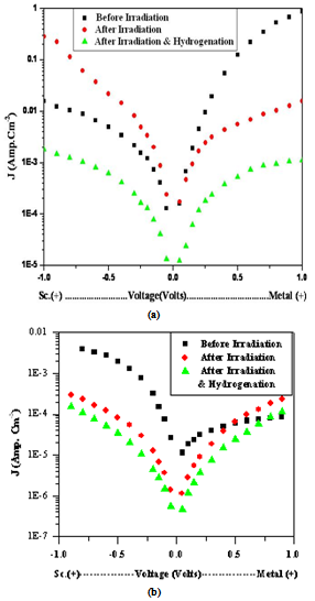 | Figure 1. J-V characteristics of (a) Pd/n-Si and (b) Pd/p-Si devices irradiated with ~100MeV gold ions of fluences1.5x1012 ions/cm2 |
3.2. C-V Characteristics
- Figure.2a shows the C-V characteristics for Pd/n-Si device before and after the irradiation with fluence 1.5x1012 cm-2. It is observed that the capacitance value decreases significantly after the irradiation with a conductivity change (from n- to p-) because the polarity of the forward and reverse bias voltage is observed to be reverted to feature the characteristics for p-type. The capacitance is observed to decrease further after the hydrogenation. The C-V characteristics of the devices prior to the irradiation also show the presence of interfacial layer of charges (Figure.2a). The dip in the reverse bias capacitance shows the presence of majority carrier deep traps whereas a dip in the forward bias reflects the presence of minority carrier deep traps[17]. In Fig.2a, the C-V characteristics feature a dip in the forward bias after the irradiation. After Hydrogenation the characteristics show a reversal of the conductivity type from p- to n- and a peak in the reverse bias. It is interesting to observe that the hydrogen seems to revert the carrier compensation caused by the radiation induced defects to bring back the radiation induced conductivity type change. The observed feature may be attributed to the hydrogen defect complexes. The observed dip of the irradiated devices correspond to deep donors (hole traps) which are localized near ~Ec – 0.69eV with a peak density ~7.2x107 cm-2. The energy level has been estimated by using the voltage value of the capacitance dip and the barrier height. The density of states has been estimated from the area of the dip on the C-V characteristics. The devices after hydrogenation (Figure.2a) show a peak which seems to corresponds acceptors localized near ~Ev + 0.13eV with density of states of ~4.6x107 cm-2. The irradiated devices (Figure.2b) show a similar reduction in capacitance (from nF to pF) and also show the conductivity type change from p-type to n-type on hydrogenation. Moreover, The C-V characteristics of the irradiated and hydrogenated devices are deviated from the usual one and show the presence of deep states (Figure. 2b). The shallow acceptor density estimated from C-2 Vs V plots, shows a reduction by two orders of magnitude after the irradiation (The linear portion of C-2 Vs V plots has been used to estimate the carrier density). The irradiated devices show a capacitance peak near the forward bias. It represents the presence of deep states which are donor type (hole trap) and the density of these traps has been estimated to be of 4.6x108 cm-2 which is located near ~Ev + 0.29eV. These devices show a conductivity type change after the hydrogenation because the C-V characteristics are observed to be reverted for the forward and reverse bias (Fig. 2b). The irradiated and hydrogenated devices were annealed in a vacuum (of ~10-3 torr) at different temperatures upto 400C for half an hour at each annealing temperature.
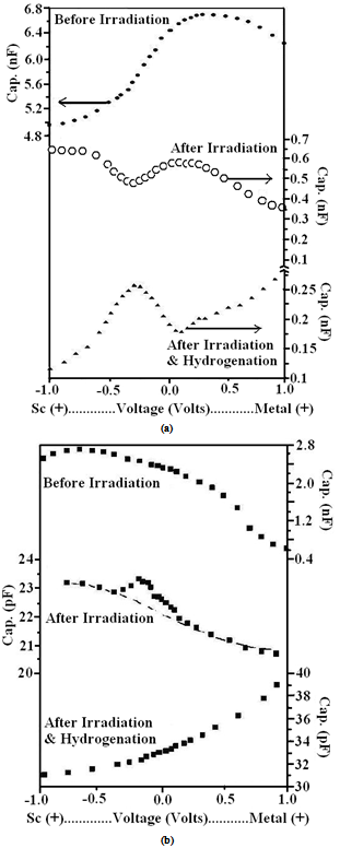 | Figure 2. C-V characteristics of (a) Pd/n-Si and (b) Pd/p-Si devices irradiated with ~100MeV gold ions of fluence 1.5x1012 cm-2 |
3.3. Infra-Red Spectroscopy
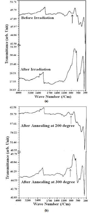 | Figure 3. I-R Spectra of Pd/p-Si devices irradiated with 100MeV gold ions of fluence 1.5x1012 cm-2 in (a) Before and After Irradiation, (b) After annealing at 200 C and 300 C[5] |
4. Discussions
- The increase in resistivity of the devices after the irradiation can be understood as decrease of majority carrier density and/or decrease of carrier mobility. Monita et al[20] have shown that the reduce in carrier mobility is limited up to some extent due to presence of radiation induced defects (acting as deep levels) but the observed increase of resistivity on the irradiation is high enough than expected from the aforesaid possible change in mobility. The loss of carriers after the irradiation is also termed as the carrier removal phenomenon due to the radiation induced defects. The radiation induced defects acting as majority carrier traps reduce the effective current carriers and hence may work as carrier removal centers. The device resistance is a series combination of metal semiconductor interface, the bulk resistance of the semiconductor substrate and the bottom ohmic contact. Thus, the observed increase in resistivity after the irradiation is a net effect of the entire device. The capacitance of the devices is controlled by the charge exchange in the depletion region spread near the metal/semiconductor interface. Carrier removal has been found to be a significant characteristic of the displacement damage[22]. It seems that the high energy heavy ions irradiation of our devices cause the displacement damage to feature the carrier removal phenomenon to increase the resistivity on the irradiation. The measured capacitance depends upon the emission of trap (e) and rate of change of applied a.c. signal (w). Most of the charge captured by ‘slow traps’ for which w>>e is retained in the depletion region during the measurement and so contribute to the measured capacitance. Whereas the fast traps traps (for which e>>w) at the measurement temperature, referred to as ‘fast traps’, do not affect the measured capacitance significantly. The observed majority carrier traps (acting as deep acceptors at Ec – 0.69eV) in gold ion irradiated devices are from a depletion depth of ~3.0µm. The density of these traps (4.7x107 cm-2) is sufficient enough to cause the observed carrier removal in the irradiated devices. It seems that it could be possible to visit these localized states by the capacitance signal of the device, because the depletion region widens deep due to the reduced capacitance (from nF to pF range) on irradiation. The depletion width (of ~3.0 µm) is shallower than the range of the irradiated ions of gold in silicon (12.81 µm from SRIM calculation). Thus the observed electronic states may be related to the damage defects caused by the electronic energy loss of the incident ions in the target lattice (of silicon).The di-vacancies can be formed by the combination of vacancies. These di-vacancies become mobile at temperatures between 200C - 300C and may complex with impurities forming VxOy complexes[23]. The mono vacancy produced by irradiation either trapped by the Oi to form V-O, annihilate by silicon or combine with other to form di-vacancy.
5. Conclusions
- The electronic properties of Pd/n-Si and Pd/p-Si devices have been studied as a function of irradiation fluence, hydrogenation and annealing temperatures. The radiation induced defects may kill/remove/compensate the carriers which reflects in decrease of current density and capacitance values. The decrease in the current density and capacitance values after irradiation reflects the widening of the depletion region. It is observed that the radiation induced defects are playing important role to change the conductivity type of devices. Decrease in electronic values of irradiated and hydrogenated devices show the compensating effect of carriers due to complexation of radiation induced defects and hydrogenation. The observed change in conductivity type is attributed to carrier removal phenomenon that may happen due to change in configuration of defect (vacancy/multi-vacancies) – hydrogen complexes. Movement of defects and defect hydrogen complex on annealing also show the net effect of carrier removal and/or carrier compensation phenomenon. It is possible that vacancy/multi-vacancy hydrogen complexes configure differently as a donor or acceptor state to cause the conductivity type change on irradiation and annealing at different temperatures. The I-R absorption studies show the absorption bands for VO, VO2 near (900 ± 20) cm-1 which has also been studied from other experimental techniques like electron paramagnetic resonance (EPR) and Infra red spectroscopy[24, 5]. The observed change in conductivity after annealing at different temperatures seems related to annealing of V-O centers which is changing its configuration with temperature.
ACKNOWLEDGEMENTS
- The authors wish to acknowledge the support and academic suggestions of our teacher Prof. P.C. Srivastava (Dept. of Physics, Banaras Hindu University, Varanasi, India). Dr. D. K. Avasthi and Dr. K. Asokan from Inter University Accelerator Center (Nuclear Science Centre), New Delhi, India is also acknowledged for support and suggestions for the irradiation work.