-
Paper Information
- Next Paper
- Previous Paper
- Paper Submission
-
Journal Information
- About This Journal
- Editorial Board
- Current Issue
- Archive
- Author Guidelines
- Contact Us
American Journal of Materials Science
p-ISSN: 2162-9382 e-ISSN: 2162-8424
2012; 2(6): 210-214
doi: 10.5923/j.materials.20120206.07
Characteristics Study of Silicon Nanoparticles Produced by Physical Vapour Deposition
 Abstract
 Reference
 Full-Text PDF
 Full-Text HTML
Wafaa M. S. Al-Khayat1, 2, Gerhard Wilde2
1Department of Physics, College of Science, Al-MustansiriyahUniversity, Baghdad, Iraq
2Institute for Material physics, University of Munster, Wilhem, Klemm-Str.10
Correspondence to: Wafaa M. S. Al-Khayat, Department of Physics, College of Science, Al-MustansiriyahUniversity, Baghdad, Iraq.
| Email: |  |
Copyright © 2012 Scientific & Academic Publishing. All Rights Reserved.
SiliconNanoparticles with thickness ranging between 40 to 50 nm and an average diameter of 80 nm were prepared by Physical Vapour Deposition (electron beam). The Nanoparticles showed blue and visible light emission from 300 Ao to 900 Ao, with peak intensity at 350-700 Ao .Also AFM measurements were carried out and the regularity of silicon Nanoparticles was calculated and found to be equal to 0.3858 according to a quantitative hexagonal regularity calculation.
Keywords: Silicon nanoparticles, PVD, Surface morphology, Photoluminescence (PL), AFM
Cite this paper: Wafaa M. S. Al-Khayat, Gerhard Wilde, "Characteristics Study of Silicon Nanoparticles Produced by Physical Vapour Deposition", American Journal of Materials Science, Vol. 2 No. 6, 2012, pp. 210-214. doi: 10.5923/j.materials.20120206.07.
Article Outline
1. Introduction
- Nanoparticles are constituted of several hundreds or thousands of atoms or molecules and can have a variety of sizes, states and morphologies (amorphous, crystalline, spheres, needles, tubes, wires, etc.).The potential impact of nanomaterial's stems directly from the small spatial and temporal scales that are involved in engineering bulk macroscopic materials and devices from Nano scaled building blocks. This, in turn, means that Nano-engineered substrates can be designed to exhibit very specific and controlled bulk chemical and physical properties as a result of the control over their molecular synthesis and assembly. As one prominent and technologically highly relevant example, the optical and electrical properties of such organized Nano crystal solid could be tuned through the characteristic nanocrystasize.Due to the reduced size of their constituent building blocks, nanostructured materials have electronic, magnetic and chemical properties, which differ considerably from those of the corresponding bulk materials For example, nanostructured materials have been found to exhibit increased strength and hardness, higher electrical resistivity, enhanced diffusivity, reduced density etc. compared to the bulk materials. Thus, these new materials are promising candidates for a variety of applications, which include heterogeneous catalysis, gas sensor technology, microelectronics, nonlinear optics, etc.Depending on the size range, shape and chemical composition of the nanoparticles, different techniques have been used for producing such samples. Among them are wet chemical processes, physical methods and combined techniques[1-3]. Silicon is a key material for the microelectronics industry. In contrast to its extensive use in electronic devices, bulk silicon has limited optoelectronic applications due to the indirect nature of its band gap. However, the development of nanostructured Si has triggered many possible avenues for the application of nanostructured silicon[4-6].Si nanoparticles: Si is the leading material concerning high density electronics. Nano structuring silicon is an efficient way to turn silicon into a photonic material. The small size results in new quantum phenomena that yield extraordinary properties Materials properties change drastically at the Nano scale because quantum confinement effects arise from the confinement of electrons and holes in the material. Moreover, at the Nano scale, short range forces such as Vander Waals forces predominate[7, 8].Silicon Nanoparticles have gained much attention as potential low-cost emitters for optoelectronics. Especially, the recent demonstration of electrical injection and optical gain makes this material highly interesting. As silicon is asemiconductor with an indirectbandgap, the role of phonons for photoluminescence is of significant relevance. However, the vibrational properties of silicon nanoparticles are strongly altered due to the nanoscopic dimensions. This is usually explained in the picture of the phonon confinement effect. While this model seems to be of some value to qualitatively asses the Raman scattering in first- order processes, it is difficult to use for scattering processes of higher order. The studyof Si nanostructures is a very active field of research because of the strong room-temperature photoluminescence (PL) and the observation of quantum size effects. A bright red PL was first observed for porous Si[9].As mentioned above, Si has an indirect band gap, which causes a very long radiated life time in the mille-second range for excited electron- hole pairs. Competing non-radiate recombination processes thus prevail and cause most of the excited electron-hole pairs to recombine non-radiative.In addition, when the number of excited electron-hole pairs increases, other non-radiated recombination processes start to play a role. Luminescent semiconductornanoparticles offer a promising opportunity to explore the photo physics and chemistry of materials in the intermediate regime between bulk and molecular behaviour. Among their many unique optical and electronic properties is the ability to obtain efficient size- tuneable photoluminescence (PL) in the visible and near visible regions of the spectrum. Recently, the group IV semiconductor Si, and to a lesser extent Ge, has received considerable interest with researchers working toward applications in the wide ranging areas of fluorescent lighting, optoelectronics or as luminescent markers for biophysical system. Here, we report on the optical characterization of ultra-small silicon Nanoparticles (Si-np) ~ 1 nm in diameter and with strong PL in the near UV-to blue. The emphasis is on their behaviour in aqueous environments as markers for biological systems[10].
2. Experimental Work
- There are two experimental components to this study. First, ultra-thin Alumina membranes (UTAM.) are prepared as masks for a subsequent deposition process.Secondly, Silicon nanoparticles were obtained by physical vapour deposition (using an electron beam evaporation system). Finally, the obtained Si nanostructures are examined by SEM, AFM and PL measurements.
2.1. Preparation of Ultra-Thin Alumina Membranes as Masks
- A carefully smoothened Al sheet was polished by applying a grinding process to obtain a mirror-like surface. Afterwards, the sheet was electro polished under constant current conditions (current =5.6A) for 3 min.Anodization was conducted under a constant cell potential condition (voltage=27V) in oxalic acid solution. After anodization, the anodic oxide film was chemically removed from the Alumina using a saturated copper chloride solution, this method carried out to removal alumina. A subsequent etching treatment was carried out in a 5 weight per cent phosphoric acid solution for42 min. This allows observing the arrangement of the pores by removing the bottom part of the anodic oxide film, i.e. the “barrier layer”. The structure of the anodic porous alumina formed under different conditions was observed from the bottom side of the film using a scanning electron microscope (SEM)[11,12]. As a well-knownNano template, alumina membranes have been widely used in fabricating different one- dimensional (1D) nanostructure, especially after the large improvement in the pore regularity of alumina membranes based on a two – step anodization process. The synthesis of ordered arrays of (1D) nanostructures benefits from the regularity of the arrayed pores of the alumina membranes with monomodal diameters. Recently, using UTAMs as the evaporation or etching masks, large scale ordered arrays of surface nanostructures (e.g., Nano dots, Nanoparticles…) have been successfully synthesized on the surface of substrates (mainly Si wafers). This UTAM surface Nano patterning technique possesses some attractive advantages such as large pattern area (>1cm2) high throughput, ultrahigh density (1010-1012 cm-2) of the surface nanostructures and low costs[13, 14].A typical UTAM on Si is shown in fig (1). The UTAM is quite thin with a thickness of about 300nm–350nm. The pore regularity of the UTAM is very high. The area of the UTAM can be as large as several square centimetres[15, 16].Figure 1 shows the surface morphology of anodic porous alumina.
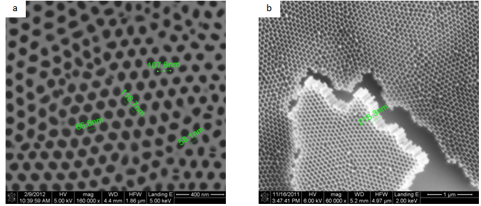 | Figure 1. SEM micrographs of anodic porous alumina a)top view b) tilted view including the cross -section |
2.2. Preparation of Si Nanoparticles
- Si nanoparticles were prepared by physical vapour deposition using an electron beam (EB) evaporationsystem. Silicon chips were placed in a graphite crucible in the electron beam chamber. A Silicon wafer was placed in the holder centred above the EB source. The chamber that was cooled by liquid nitrogen was evacuated to a base pressureof (2*10-6mbar). The process of Si nanoparticle preparation takes 8h- 12h, depending on the deposition rate. After this step, the UTAM mask was completely removed to obtain the free-standing Si nanoparticles[17-24].
3. Resultsand Discussion
3.1. Photoluminescence (PL)
- Photoluminescence (PL) spectroscopy is an important tool to study the excited electronic states in solids. The PL intensity is determined by the population density of excited states and the quantum yield. Therefore, PLmay provide information on the relaxation dynamics of excited states. Measuring PLfrom distinctly populated excited electronic states enables, for instance, to examine effects from electron-electron interaction.The absorption spectrum of a material contains all possible transitions while photoluminescence involves emission of a particular wavelength that corresponds to the respective transition. Photoluminescence occurs when an excited state relaxes to the initial state by releasing the energy difference of the two states involved through photon emission. The process can be direct or indirect depending on the electronic band structure[7].This section focuses on the PL result obtained on the Si nanoparticles deposited on the silicon surface. Figure 2 displays the PL spectra of Si nanoparticles measured at room temperature. All plots extend to cover blue and red emissions. The fact that distinct peaks are not observed might be related to the substrate or to size confinement effects[25-27].
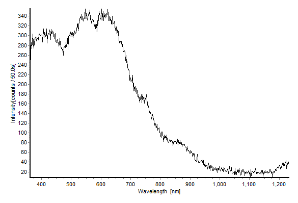 | Figure 2. Photoluminescence spectrum of Si nanoparticles on a Si wafer |
3.2. Scanning Electron Microscopy (SEM)
- Characterization of the Si nanoparticle’s structure had been conducted using scanning electron microscopy (SEM) and atomic force microscopy (AFM) in order to gain understanding of their formationmechanism. The most challenging task in preparing Si- Nanoparticles is to succeed in controlling the particle size and morphology as well as the surface properties[28].Figure 3 shows scanning electron micrographs of the deposited Si nanoparticles prepared by electron beam deposition. The Si wafer substrates were placed directly above the target. The sample generated at 2*10-6mbar showed a rough surface structure composed of Si nanoparticles.
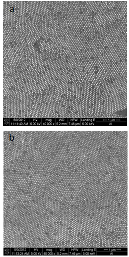 | Figure 3. SEM plane view of Si Nanoparticles a) atdeposition rate of 0.2(Ao/sec). b) atdeposition rate of 0.1(Ao/sec) |
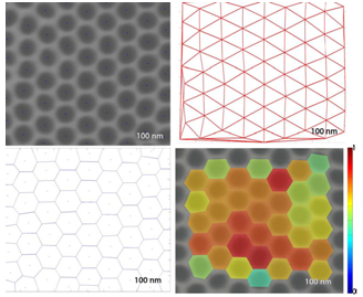 | Figure 4. Principle of the regularity analysis, depending on the Voronoi tessellation |
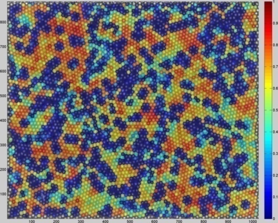 | Figure 5. Regularity analysis of Nanoparticles |
 The calculated hexagonal regularity, which equals R = 1 for perfect hexagonal order is equal to:RSi = 0.3858This value corresponds to a medium regularity with the size of the hexagonally ordered regions that span about the first and second nearest neighbour shells.The atomic force microscope produces topological images of surfaces at very highmagnification and it is even possible to observe the atomic structure of crystals. The aim of this study with the atomic force microscope is to obtain information about the formation of the surface. The morphology of the Si-nanoparticles film is very sensitive to the deposition parameters, such as the deposition rate, the position of the substrate and the regularity of the UTAM mask.
3.3. Atomic Force Microscopy (AFM):
- The AFM images shown in Figure (6) have been analysed using the software “Gwyddion”. Line profiles were employed to estimate the size and height of the nanoparticles. The nanoparticle density has been calculated by counting particles in the window using the image processor.
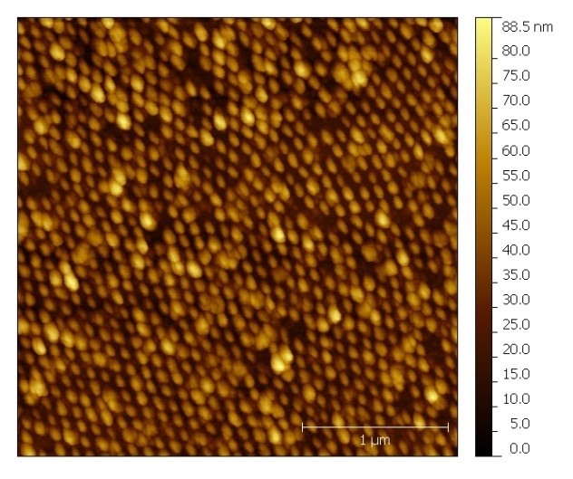 | Figure 6. AFM image of Si nanoparticles |
4. Conclusions
- 1. Ultra-Thin Alumina Membranes (UTAMs) with an almost ideal ordered honeycomb structure could be obtained in oxalic acid solution, time of opening pores and anodic voltage effect on arrays regularity.2. The large scale ordered arrays of quantum –sized surface structures are promising candidate structures for new types of optoelectronic and display devices on the basis of the quantum confinement effect.3. The photolumince (PL) spectra at room temperature revealed a broadband spectrum in a range 350nm to more than 700nm.4. The SEM images show array of Si Nanoparticles.5. Results show that the film morphology could be controlled by different parameters like UTAMs mask regularity and deposition rate.6. The morphological study of the deposition Si Nanoparticles that is revealed from the AFM analysis depends on Quantitative Hexagonal Regularity Calculation principles show the calculated hexagonal regularity which equals R=1 for perfect hexagonal order is equal to :Rsi=o.3858.