-
Paper Information
- Next Paper
- Previous Paper
- Paper Submission
-
Journal Information
- About This Journal
- Editorial Board
- Current Issue
- Archive
- Author Guidelines
- Contact Us
American Journal of Materials Science
p-ISSN: 2162-9382 e-ISSN: 2162-8424
2012; 2(6): 179-184
doi: 10.5923/j.materials.20120206.04
Design and Simulation of MEMS Based Piezoelectric Shear Actuated Beam
 Abstract
 Reference
 Full-Text PDF
 Full-Text HTML
K. Srinivasa Rao1, G. Srinivas2, M V V K Srinivas Prasad2, Y. Srinivas3, B. Shudheer4, A Venkateswar Rao5
1Department of Electronics & Instrumentation, Lakireddy Bali Reddy College of Engineering (Autonomous), Mylavaram-421230, A.P, India
2Department of Physics, KL University, Vadeswaram, Guntur District, Andhra Pradesh, India
3Department of Computer Science Engg, GITAM University, Hyderabad Campus, A.P, India
4Department of Mechanical Engineering, Lakireddy Bali Reddy College of Engineering (Autonomous), Mylavaram-421230, A.P, India
5Department of Physics, DNR College, Bhimavaram, A.P, India
Correspondence to: K. Srinivasa Rao, Department of Electronics & Instrumentation, Lakireddy Bali Reddy College of Engineering (Autonomous), Mylavaram-421230, A.P, India.
| Email: |  |
Copyright © 2012 Scientific & Academic Publishing. All Rights Reserved.
Now-a-days, there has been growing demand for the development of micro scale devices, due to its less cost, space requirements, high dimensional stability and especially manufacturing time. This paper reports the modeling of MEMS based Piezoelectric shear actuated beam by using COMSOL Multiphysics software of version 4.2a.The dimensions of the model beam is of 100-mm long, 30-mm width, 10-mm thickness. In this paper, we analysed the deflection of beam under different voltages. In the first step, deflection of beam is analysed by changing the material of sandwiched beam. In the second step deflection of beam is explored by changing material of electrodes. In the third step, deflection of beam is analysed by changing both materials of sandwiched beam and electrodes. In the final step defection of beam is explored by changing both thickness and material of electrodes. Finally, the results of analysis allowed to conclude us to design a piezo electric shear actuated beam with different ranges and resolutions, under the condition of changing both thickness and material of electrodes gives the optimum deflection of 216nm under 30v excited input voltage.
Keywords: MEMS, Sensor, Actuator, Piezoelectric Beam
Cite this paper: K. Srinivasa Rao, G. Srinivas, M. S. Prasad, Y. Srinivas, B. Shudheer, A Venkateswar Rao, "Design and Simulation of MEMS Based Piezoelectric Shear Actuated Beam", American Journal of Materials Science, Vol. 2 No. 6, 2012, pp. 179-184. doi: 10.5923/j.materials.20120206.04.
Article Outline
1. Introduction
- MEMS is a process technology used to create tiny integrated devices or systems that combine mechanical and electrical components. They are fabricated using integrated circuit (IC) batch processing techniques and can range in size from a few micrometers to milli meters. These devices (or systems) have the ability to sense, control and actuate on the micro scale, and generate effects on the macro scale[1].The interdisciplinary nature of MEMS utilizes design, engineering and manufacturing expertise from a wide and diverse range of technical areas including integrated circuit fabrication technology, mechanical engineering, materials science, electrical engineering, chemistry and chemical engineering, as well as fluid engineering, optics, instrumentation and packaging. The complexity of MEMS is also shown in the extensive range of markets and applications that incorporate MEMS devices. MEMS can be found in systems ranging across automotive, medical, electronic, communication and defence applications. Current MEMS devices include accelerometers for airbag sensors, inkjet printer heads, computer disk drive read/write heads, projection display chips, blood pressure sensors, optical switches, micro valves, biosensors and many other products that are all manufactured and shipped in high commercial volumes[2-4]. MEM has been identified as one of the most promising technologies for the 21st Century and has the potential to revolutionize both industrial and consumer products by combining silicon based microelectronics with micromachining technology. Its techniques and micro system based devices have the potential to dramatically affect of all of our lives and the way we live[5-8].In this paper, we designed and simulated MEMS based piezoelectric shear actuated beam by using COMSOL Multiphysics software of version 4.2a
2. Geometry of Model
- The model consists of a 100-mm long sandwiched cantilever beam. This beam is composed of a 2-mm thick flexible foam core sandwiched by two 8-mm thick aluminium layers. Further, the device replaces part of the foam core with a 10-mm long piezoceramic actuator that is positioned between x=55 mm and x=65 mm. The cantilever beam is orientated along the global x-axis.B OUN D A R Y C O N DI T I O N S:
 | Figure 1. Geometry of model |
2.1. Material Properties
- The following table gives the properties of materials used in the model:
|
2.2. Design Procedure
- The modeling mems based piezoelectric shear actuated beam is done in the COMSOL MULTIPYSICS software. In this, first piezoelectric devices present in structural mechanics module in the ADD PHYSICS tree. Then we have to select STUDIES in preset studies. The next step is to construct geometry of the beam, which consists of three blocks of 100-mm long each with different thickness. The next step is to define co-ordinate system as base vector system.The next is to do physical interface i.e., to add material to that model and to specify values of properties of that materials. Then we have defined fixed constraints, electric potential and ground boundaries. Then mesh of the model has to build. Then compute the model by and get displacement plot as follows:The same model can be simulate by changing voltages, materials and can observe for displacement plots.
2.3. Simulations
- The following simulations are done on the model of piezoelectric shear actuated beam:
 | Figure 2. Deflection plot |
2.3.1. Simulation-1 for Pzt-5h and Al
- In this pzt-5h as piezoceramic material and aluminium as electrodes are taken and compute by applying 10V, 20V, 30v. The displacement plots are as follows:
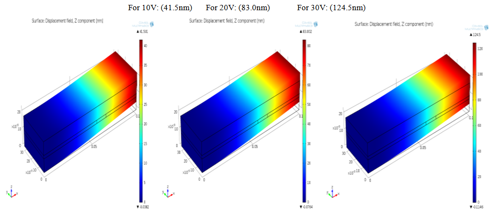 | Figure 3. Deflection plot for simulation-1 |
2.3.2. Simulation-2 for Pzt-5h and Cu
- In this pzt-5h as piezoceramic material and copper as electrodes are taken and compute by applying 10V, 20V, 30v. The displacement plots are as follows:
 | Figure 4. Deflection plot for simulation-2 |
2.3.3. Simulation-3 for Barium Titanate and Cu
- In this barium titanate as piezoceramic material and copper as electrodes are taken and compute by applying 10V, 20V, 30v. The displacement plots are as follows:
 | Figure 5. Deflection plot for simulation-3 |
2.3.4. Simulation-4 for Barium Titanate and Al
- In this barium titanate as piezoceramic material and aluminium as electrodes are taken and compute by applying 10V, 20V, 30v. The displacement plots are as follows:
 | Figure 6. Deflection plot for simulation-4 |
2.3.5. Simulation-5 for Pzt-5h and Cu with 4-Mm Thickness
- In this pzt-5h as piezoceramic material and 4-mm thickness copper as electrodes are taken and compute by applying 10V, 20V, 30v. The displacement plots are as follows:
 | Figure 7. Deflection plot for simulation-5 |
3. Results and Discussions
- The analysis from the above table is as follows:●With increase in voltage the deflection of the beam increases but beyond 30V the model becomes unstable. So we can apply voltage up to 30V.●The piezoceramic material, lead zirconate titanate gives high shear than any other piezoceramic material and also with decrease in the thickness of electrodes and using copper, high electrical conductivity material than aluminium gives maximum shear in the beam.● Thus, for the application of actuator, which requires deflection particularly 216nm, this model with piezoceramic material of PZT-5H of 2-mm thickness and copper electrodes of 4-mm thickness can be used.The deflection plot with optimum displacement is as follows;
 | Figure 8. Deflection plot |
4. Conclusions
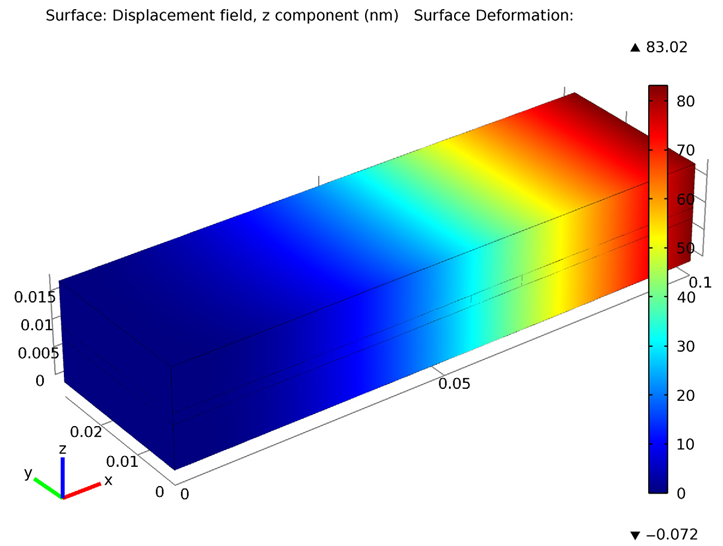
- The conclusion to this paper is that with the model-“PIEZOELECTRIC SHEAR ACTUATED BEAM” having 4-mm thickness of copper electrodes and 2-mm thickness PZT-5H when excited by 30v gives optimum deflection of 216 nm when compared to the model of 8-mm thickness aluminium electrodes and 2-mm thickness PZT-5H when excited by 20v gives a deflection of 83 nm. The material selection and dimensions of a user specific mems based Piezo electric shear actuated beam are selected with optimized range and resolution. Thus this actuating operation finds a usage specifically in an application which needs a deflection of 216nm.
ACKNOWLEDGEMENTS
- The author Dr.K.Srinivasa Rao would like to thank IISc, Bangalore, for providing research facilities under NPMASS Scheme. The authors also would like to thank the director and The Management of Lakireddy Bali Reddy College of engineering for constant encouragement for the development of MEMS Technology. The author is very thankful to anonymous referee of this paper for valuable suggestions and comments, which greatly help to improve the quality of this paper.
References
| [1] | Micro electro mechanical systems by Dennis M. Freeman; The MEMS handbook edited by Mohammad Gad-El-Hak University of Notre Dame. |
| [2] | K.Srinivasa Rao et;al, Advances in Applied Science Research, 2(6), 570-579 (2011); Archives of Physics Research, 2(4), 158-165 (2011) |
| [3] | Micro Electro-Mechanical Systems, Advanced materials & Fabrication methods. (1997) NMAB-483, National academy press, Washington, D.C. 1997. |
| [4] | V. Piefort, Finite Element Modeling of Piezoelectric Active Structures, Ph.D. thesis, University Libre de Bruxelles, Belgium, Dept. Mechanical Engineering and Robotics, 2001. |
| [5] | A. Benjeddou and others, A Unified Beam Finite Element Model for Extension and Shear Piezoelectric Actuation Mechanisms, CNAM (Paris, France), Structural Mechanics and Coupled Systems Laboratory, 1997. |
| [6] | Benjeddou, A., Trindade, M. A. & Ohayon, R., 1998, ‘A new shear actuated smart structure beam element’, AIAA 98-1922. |
| [7] | Cady, W. G., 1946, Piezoelectricity; an Introduction to the Theory and Applications of Electromechanical Phenomena in Crystals, Mc Graw-Hill, New York, London. |
| [8] | Crawley, E. F. & Anderson, E. H., 1989, ‘Detailed models of piezoceramic actuation of beams’, AIAA 89-1388-CP. |