-
Paper Information
- Previous Paper
- Paper Submission
-
Journal Information
- About This Journal
- Editorial Board
- Current Issue
- Archive
- Author Guidelines
- Contact Us
American Journal of Materials Science
p-ISSN: 2162-9382 e-ISSN: 2162-8424
2012; 2(5): 160-164
doi: 10.5923/j.materials.20120205.05
Cuinse2 Solar Cells Efficiency Optimization
 Abstract
 Reference
 Full-Text PDF
 Full-Text HTML
N. Touafek 1, 2, M. S. Aida 1, R. Mahamdi 3
1Laboratoire Couches minces et Interface Faculté des Sciences, Université de Constantine, 25000, Algerie
2Département d’Electronique, Faculté des Sciences de l’Ingénieur, Université de Constantine, 25000, Algerie
3Département d’Electronique, Faculté de Technologie, Université Hadj Lakhdar Batna, 05000, Algerie
Correspondence to: M. S. Aida , Laboratoire Couches minces et Interface Faculté des Sciences, Université de Constantine, 25000, Algerie.
| Email: |  |
Copyright © 2012 Scientific & Academic Publishing. All Rights Reserved.
In the present paper calculation of CuInSe2(CIS)/CdS solar cell efficiency is presented. The influence of the thickness and the optical band gap of CdS and CIS layers on the solar cell performances are investigated. The thickness of CdS buffer layer, which is generally neglected is taken into account. The solar cells performances calculations are based on the calculation, by means of developed software written with Matlab, of photocurrent from the resolution of the well known three coupling equations: continuity equation for holes in the CdS (n-region) and for electrons in the CIS (p- region) and Poisson equation. The obtained results indicated that the solar cell efficiency can be improved by reducing the CdS thickness or by increasing the CIS thickness. The efficiency increasing rates are 0.01 %/ nm and 0.5 %/nm for CdS and CIS layer thickness respectively. The CdS layer alters the shorter wavelength of the solar spectrum, while the CIS layer alters the longer wavelength. CIS layer optical band gap is the most crucial parameter by comparison to the optical gap of CdS layer.
Keywords: Solar Cell- Cuinse Photovoltaic-Thin Films
Cite this paper: N. Touafek , M. S. Aida , R. Mahamdi , "Cuinse2 Solar Cells Efficiency Optimization", American Journal of Materials Science, Vol. 2 No. 5, 2012, pp. 160-164. doi: 10.5923/j.materials.20120205.05.
Article Outline
1. Introduction
- During the last years solar cells based on CuInSe2 (CIS) has emerged as a potential candidate for low cost thin films solar cells production. The 19.5 % efficiency obtained in ZnO/CdS/CIS[1] hetrostructure is encouraging and is considered as an interesting stimulant for the development of thin film solar cells technology. Currently CIS solar cells have attracted interest for spatial applications because of the stability of CIS solar cells against electron and proton irradiation then silicon or III-V semiconductors.There is a worldwide effort to reduce the material for solar cells production with a higher ratio power on weight. The reduction of different active layers thicknesses will have two direct consequences: (i) the reduction of solar cell cost and (ii) the use of less scare material; such as In and harmful and toxic ones such as Se and Cd on the other hand . Thereafter, the thickness is an important parameter to study and to optimize its influence on solar cells properties. Actually most studies made on CdS/CIS solar cells are mainly experimental, due to the fact that researchers are interested much more in experimental work to the detriment of the theoretical research which remains always insufficient. However calculation is a simple method, economic and it saves effort and time to optimize solar cells technological parameters ( layer thickness, material optical gap, doping ..etc). The merit of numerical study is to test and predict the results and the influence of the process parameters on the device without fabrication. The present paper deals with the numerical study of the influence of CdS layer thickness on the performance of CIS based solar. Generally the absorption in CdS layer is neglected, however it can contribute in short wavelength available in the sun spectrum[2]. Since the optical band gap of the CIS layer can be tailored by controlling the deposition parameters[3-6], the influence of CIS absorber layer and its optical band gap is also investigated. The solar cell efficiency and spectral response dependence on the thickness and optical band gap of both CdS and CIS layers are investigated to determine the factor limiting the cell performance.
2. Calculation Procedure
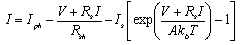
- In this study, the cell is made up of a stacking of thin layers ZnO/CdS/CuInSe2. ZnO layer is a highly conducting window used as transparent electrode. The heterojunction partner are the n- type CdS layer and the p-type CuInSe2 layer . A schematic drawn of the cross section and the band diagram structure of the device are shown in figure 1. We have developed a software by the Matlab language run on a PC computer. The photocurrent is calculated from the resolution of the well known three coupling equations: continuity equation for holes in the CdS (n-region) and for electrons in the CIS (p- region) and Poisson equation. The determination of the efficiency of the cell was carried by considering the real electrical model of a solar cell (as a diode in parallel to a courant generator, series and shunt resistance). The output I current in this model is expressed by the following empirical relation:
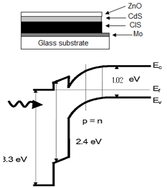 | Figure 1. (a) a schematic cross section and (b) band diagram of the hetrostructure forming the studied CIS solar cell |
 Vm and Im are respectively the voltage and current of the maximum operating point , Pin is the incident sun power.
|
3. Results and Discussions
3.1. Influence of CdS Thickness Layer
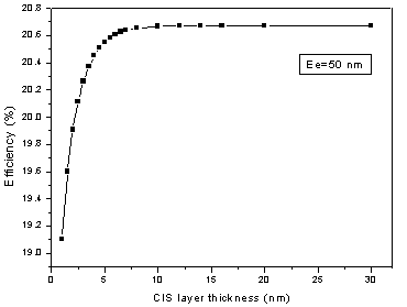
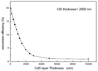 | Figure 2. The variation of CIS solar cell efficiency as a function of the window layer thickness |
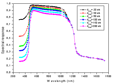 | Figure 3. The variation of CIS solar cell quantum efficiency as a function of the incident wavelength for different CdS layer thickness for a fixed absorber layer thickness equal to 2000 nm |
 | Figure 4. The variation of the CIS solar cell efficiency as a function of the absorber layer thickness |
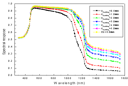 | Figure 5. The variation of CIS solar cell quantum efficiency as a function of the incident wavelength for different CIS layer thickness for a fixed window layer thickness equal to 50 nm |
3.2. The Influence of Cuinse2
- For mass production the reduction of the layer thickness reduces the amount of material consumption (especially scarce ones such as In) and then solar cell cost. Current research has focused on reducing the absorber layer thickness without adversely altering the solar cell performances. This explains the importance of the study of influence of absorber thickness upon the solar cell efficiency. In figure 4 we have reported the calculation results of the efficiency as function of absorber layer thickness with a fixed the window layer thickness at 50nm. In the range of 1 to 6000nm CIS thickness, the solar cell efficiency increases linearly with a rate of 0.5% /nm. However further increase in the CIS thickness beyond 6000 nm do not improve the efficiency, this is due to the high absorption coefficient of CIS, 6000 nm is enough to absorb all the solar spectrum incident photons. The influence of the absorber layer come from its influence mainly in the short wavelength region of the visible spectrum, as can deduced from the variation of the quantum efficiency reported in figure 5. This is due to the low band gap of the CIS material.As seen in figures 3 and 5, the CdS and CIS thickness layer alter the quantum efficiency of solar cells. CdS layer affects the shorter wavelength of the visible spectrum, while the CIS layer affects the longer wavelength region. It worth noting that the available solar spectrum is not symmetrical, the maximum intensity is located around 1.8 eV, which is closer to the CIS optical gap than to CdS optical gap. This explains the larger influence of CIS thickness upon the solar cell quantum efficiency.
3.3. Influence Of The CIS and Cds Optical Gaps
- The optical gaps of CdS and CIS can be varied when prepared as thin films. Several techniques have been used to prepare CdS thin films namely: sputtering[8] , thermal evaporation[9] electrodeposition[10], spray pyrolysis[11] and chemical bath deposition (CBD)[12]. Each technique have its specification but as well as for other physical properties, the optical gap can be tailored with varying the deposition parameters (substrate temperature, power, temperature, molarity or pH of solution). CIS thin film can be also prepared by a variety of different fabrication techniques, such as vacuum evaporation[13], flash evaporation[14], molecular beam epitaxy[15], sputtering [16–21], electrodeposition[22] and selenization of Cu–In precursors[23,24]. As well as for CdS its optical gap can be controlled by the deposition parameter and also by adding amount of Ga and S. Alloying with Ga[25], Al[26] or S[27] increases the bandgap of CuInSe2 and makes it more suitable for high-efficiency devices. Solar cells are fabricated using CIS alloys cousin such as: Cu(In,Ga)Se2 (CIGS) and Cu(In,Ga)(Se,S)2, which have higher band gaps (to about 1.2 eV compared to 1.04 eV for CIS) . An increase in the band gap resulted in the production of high-performance solar cells with efficiencies of 19.2% for small-area[28]. The relationship between absorber energy gap and the open-circuit voltage and device efficiency for a large variation in Ga content show that open circuit voltage Voc scales linearly with optical gap Eg over a wide range (up to 1.4eV) of Ga concentration, but the efficiency decreases when Eg is greater than 1.25 eV[25]. We have investigated the influence optical band gap of both window and absorber layers. In figures 6.a and b we have reported the variation of the solar cell efficiency as a function of CdS ( figure 6.a) and CIS optical gaps (figure 6.b). We have considered a thickness equal to 50 nm for the front layer and to 2000 nm for the absorber layer. We have varied the CdS layer band gap in the range (2,42 -2,54 eV) and CIS band gap layer in the range (0,95 -1,20eV) . These ranges are chosen after a synthesis of compiled data from the literature[29, 30]. As can be see, the influence of CdS optical gap on the efficiency is insignificant. However the optical gap of the absorber layer is more decisive. The efficiency increases linearly with the optical gap of CIS layer. It reaches the value of 27% for a gap of 1.20 eV. It approaches the theoretical optimum for the conversion of the solar energy[31] .
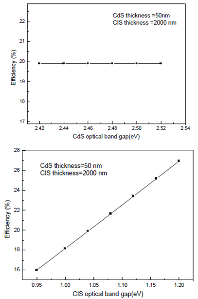 | Figure 6. Variation of CIS solar cell efficiency as a function of (a) CdS layer optical band gap and (b) CIS optical band gap |
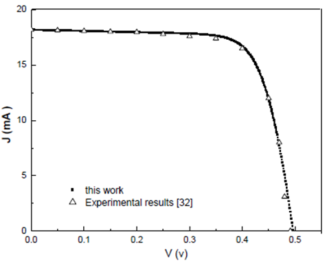 | Figure 7. Calculation results of current-voltage characteristic of CIS solar cell compared with experimental results |
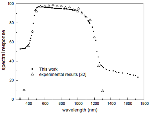 | Figure 8. Calculated quantum efficiency of CIS solar cell compared with experimental results |
4. Conclusions
- In the present work we have carried a numerical investigation of the thicknesses and optical gap of CdS and CIS layers used in CdS/CIS solar cell . The obtained results indicates that the reduction in CdS window layer thickness enhances the solar cell efficiency with a rate of 0.01% /nm. The cell efficiency is more sensitive to the absorber layer thickness, an increase in CIS thickness enhances the efficiency with the rate 0.5%/ nm . However, the cell efficiency saturates beyond 6000 nm CIS thickness. The CdS thickness alters only the short wavelength response of the solar cell, while the absorber layer alters the longer wavelength region. We have concluded also that CdS optical gap influence on cell efficiency is insignificant. A slight decrease in the cell efficiency follows an increase in CdS optical. The influence of CIS optical gap is more crucial. The solar cell efficiency increases linearly with the optical gap. The calculated results are in god concordance with the experimental ones. From our calculations we concluded that an efficiency as high as 27% can be achieved in CIS solar cell formed with CIS optical gap equal 1.2 eV and thickness of 2000 nm and 50 nm CdS layer thickness.
References
| [1] | M.A. Contreras, K. Ramanathan, J. AbuShama, F. Hasoon, D.L. Young,B. Egaas, R. Noufi, Prog. Photovoltaics 13 (2005) 209. |
| [2] | A.Mordes –Acerto energy procedia 2(2010)169 |
| [3] | J. Muller, J. Nowoczin, H. Schmitt Thin Solid Films 496 (2006) 364. |
| [4] | Tomoaki Terasakoa,_, Yuji Unoa, Tetsuya Kariyab,Sho Shirakata Solar Energy Materials & Solar Cells 90 (2006) 262 , |
| [5] | A. Bouraiou, M.S. Aida, O. Meglali, N. Attaf to be published in Current Applied Physics (in press) |
| [6] | Z. Zhang, J. Li, M.Wang, Mi. Wei, G. Jiang, C.i Zhu Solid State Communications 150 (2010) 2346] |
| [7] | Karl W. Boer, Energy Conversion and Management 52 (2011) 426 |
| [8] | J.Pouzet, J.C.Benede, A.Khellil, H.Essaidi and S. Benhida, Thin Solid Films 208(1992)252. |
| [9] | R. Inov and D.Desheva, Thin Solid Films213(1992)230. |
| [10] | R.P.Raffaelle,H.Forsell,T.Potdevin,R.Fridefeld,J.G.mantovani,S.G.Bailey,S.M. Hubbard, E.M. Gordon and A.F. Hepp, Sol. Energy Mater. Sol. Cells 57(1999)167. |
| [11] | K.Subba Ramaiah and V. Sundara Raja, Sol. Energy Mater. Sol.Cells 32(1994)1 |
| [12] | M.T.S. Nair, P.K. Nair, R.A.Zingaro and E.A.Meyers,J.Appl.Phys.75(1994)1557 |
| [13] | L.L. Kazmerski, M.S. Ayyagari, F.R. White, G.A. Sanborn, J. Vac. Sci.Technol. 13 (1976) 139. |
| [14] | B. Schumann, H. Neumann, E. Nowak, G. Ku¨ hn, Cryst. Res. Technol. 16(1981) 675. |
| [15] | S.P. Grindle, A.H. Clark, S. Rezaie Serej, E. Falconer, J. McNeily, L.L.Kazmerski, J. Appl. Phys. 51 (1980) 5464. |
| [16] | T. Yamaguchi, J. Matsufusa, H. Kabasawa, A. Yoshida, J. Appl. Phys. 69(1991) 7714. |
| [17] | T. Tanaka, Y. Demizu, T. Yamaguchi, Jpn. J. Appl. Phys. 35 (1996) 2779. |
| [18] | T. Tanaka, N. Tanahashi, T. Yamaguchi, Sol. Energy Mater. Sol. Cells 50(1998) 13. |
| [19] | T. Tanaka, T. Yamaguchi, A.Wakahara, Thin Solid Films 343– 344 (1999)320. |
| [20] | J.L. Hernandez-Rojas, M.L. Lucia, I. Martil, G. Gonzalez-Diaz, J.Santamaria, F. Sanchez-Queseda, Appl. Opt. 31 (1992) 1606. |
| [21] | S. Isomura, H. Kaneks, S. Tomioka, I. Nakatni, K. Musumoto, Jpn. J.Appl. Phys. 19 (1980) 23. |
| [22] | A.M. Fernandez, P.J. Sebastian, R.N. Bhattacharya, R. Noufi, M.Contreras, A.M. Hermann, Semicond. Sci. Technol. 11 (1996) 964. |
| [23] | T. Nakada, A. Kunioka, Jpn. J. Appl. Phys. 37 (1998) L1065. |
| [24] | S. Zweigart, S.M. Sun, G. Bilger, H.W. Schock, Sol. Energy Mater. Sol.Cells 41/42 (1996) 219 |
| [25] | W.N. Shafarman, R. Klenk, B.E. McCandless, J. App. Phys. 79(1996)7324 |
| [26] | P.D. Paulson, M.W. Haimbodi, S.Marsillac, R.W. Birkmire, W.N. Shafarman. J. Appl. Phys. 91(2002) 10153. |
| [27] | M .Engelmann, B.E. McCandless, R.W. Birkmire. Thin Solid Films 387(2001) 14. |
| [28] | S., Wagner, J.L., Shay and H.M. Kasper, Appl. Phys.Lett., 27(1975), 89. |
| [29] | C. Deokjoon, N. K. Huang, K. Sunmi, , Journal of Wuhan University of Technology, vol.19,(2004) 1. |
| [30] | G. Pankaj and J. C. Garg, Thin Solid Films, 192(1990)L5. |
| [31] | A.Jehad, A. AbuShama, R. Noufi, Steve Johnston, Scott Ward, X. Wu, Proceedings of the 31st IEEE Photovoltaic Specialists Conference, Lake Buena Vista, Florida, 2005. |
| [32] | A.Jehad A.M.Abushama, S.Johnston, T.Moriarty, G.Teeter, K.Ramanathan and R.Noufi. Progress inphotovoltaics :Research and Applications 12(2004)39. |