-
Paper Information
- Previous Paper
- Paper Submission
-
Journal Information
- About This Journal
- Editorial Board
- Current Issue
- Archive
- Author Guidelines
- Contact Us
American Journal of Materials Science
p-ISSN: 2162-9382 e-ISSN: 2162-8424
2012; 2(4): 131-137
doi: 10.5923/j.materials.20120204.06
Optical Properties of 3,4,9,10-Perylenetetracarboxylic Diimide (PTCDI) Organic Thin Films as a Function of Post-Annealing Temperatures
 Abstract
 Reference
 Full-Text PDF
 Full-Text HTML
M. El-Nahhas 1, H. Abdel-Khalek 2, E. Salem 2
1Physics department, Faculty of Education, Ain Shams University, Roxy 11757, Cairo, Egypt
2Physics Department, Faculty of Science, Suez Canal University, Ismailia, Egypt
Correspondence to: E. Salem , Physics Department, Faculty of Science, Suez Canal University, Ismailia, Egypt.
| Email: |  |
Copyright © 2012 Scientific & Academic Publishing. All Rights Reserved.
In this work, effect of post-annealing on the structural and optical properties of thermally evaporated PTCDI films deposited on quartz substrates is reported. The optical properties were investigated using spectrophotometric measurements in wavelength range 200-2500 nm for as-deposited and annealed films with the same thickness at different temperatures. The XRD studies confirm the films have orthorhombic structure (PNA21) space group. The optical constants were accurately determined using reflectance and transmittance spectra. The dispersion of the refractive index is discussed in terms of single oscillator model. In addition, the ratio of free carrier concentration to its effective mass was estimated. The absorption analysis has been also performed in order to determine the type of electronic inter-band transitions for the films. Both direct and indirect transitions are present. The direct and indirect bandgap energy decreases with increasing temperature. The decrease in the energy can be explained by increase of delocalized π electrons due to thermal annealing.
Keywords: Organic Thin Films, Optical Properties, Solar Cell
Article Outline
1. Introduction
- A great increase in demand for low cost, high effect solar cell has intensified research into improving current technology and developing cutting-edge next generation photovoltaic devices. Today, most commercial solar cells are made from silicon. Like many conventional semiconductors, silicon offers excellent, well-established electronic properties. However, the use of silicon or other conventional semiconductors in photovoltaic devices has been limited by the high cost of production. The fabrication of even the simplest semiconductor cell is a complex process that has to take place under tightly controlled conditions, and for this reason researchers have long considered organic alternatives. Organic semiconductors can often be made a flexible, lightweight and inexpensive form of solar cells. The technology for these solar cells is progressing and they are gaining popularity due to their environmentally safe composition. Research into new technologies for the development of next generation photovoltaic has focused on the research and technical development of organic devices.Extended and π-conjugated organic semiconductors have received much attention due to their excellent electronic performances. For example, the fluorescent dye 3,4,9,10- Perylenetetracarboxylic diimide or PTCDI is used extensively as an industrial pigment, because of its brilliant colour, strong absorption and fluorescence, and good thermal, chemical, and photochemical stability[1-4]. PTCDI and its derivatives are effective n-type organic semiconductors with various applications. For example, they are used as tunable laser dyes, light-harvesting materials, transistors, molecular switches, solar cells, and optoelectronic devices, such as light-emitting diodes, because of their unique optical and electrochemical properties[5-10]. There are indications that derivatives of perylenetetracarboxylic acid favour charge transfer due to large intermolecular coupling, and this may lead to the formation of charge transfer excitons[11,12].Optical properties of active layer in solar cell are considered as trivial factor. Generally, it is believed that annealing can improve the crystallization and orientation of organic layer and influenced organic photovoltaic device efficiency significantly. Under thermal annealing processing, the refractive index (n) and extinction coefficient (k) of the active layer varies with distinct temperature. Through the optical constant variation, optical property of the multilayer system (solar cell) can be optimized. Therefore, Post-growth annealing has been proved to be an efficient approach to improve crystalline quality and optical properties of organic thin films. In this work, post-growth annealing was performed on 3,4,9,10-Perylenetetracarboxylic diimide thin films grown by thermal evaporation at room temperature. Ex situ optical spectroscopic measurements were performed to investigate the optical properties of annealed PTCDI thin films.
2. Experimental Details
- Different PTCDI films with the same thickness of 400 nm were prepared by conventional thermal evaporation technique at a pressure of
 . Purified PTCDI powder (99.99% Sigma Aldrich Co.) was loaded into a molybdenum cell with nozzle of 5 mm in diameter on the top. The flat quartz substrates were located above 15 cm from the source. The substrates were carefully cleaned by putting them in chromic acid for 20 min and then they were washed several times with distilled water. After that the substrates were rinsed by isopropyl alcohol. The substrates were dried in a steam of dry nitrogen, and finally were cleaned by atomic bombardment in an initial stage of evacuation. The film thicknesses were controlled by using a quartz crystal thickness monitor and subsequently calibrated interferometrically by Tolansky’s method[13]. All films were deposited at room temperature and the rate of deposition was 2.5 nm/s. After deposition, several films have been annealed at different temperatures under vacuum (
 ) for two hours.Room temperature XRD measurements (X'Pert PRO Philips X-ray diffractometer) were carried out using
  radiation in the (
 ) geometry. The spectra of the films were scanned over the range of 5o to 90o (2
 ), with a step rate of 0.02o (2
 ) and a fixed counting time of 10s for each step, in order to obtain spectra with sufficient signal to noise ratio. The transmittance
  and reflectance
  spectra of both as-deposited PTCDI and annealed films were measured at normal incidence at room temperature in the spectral range 200–2500 nm by using a computer-aided double-beam spectrophotometer (JASCO model V-570 UV–VIS-NIR). A blank quartz substrate was used as a reference for the transmittance scan. In order to calculate the refractive index (n) and the absorption index (k) of the thin films at different wavelengths, the following equations were applied:
 | (1) |
 | (2) |
 | (3) |
3. Results and Discussion
3.1. Structural Investigation
- Figure 1 shows the X-ray diffraction (XRD) spectra of the powder, the as-deposited and the annealed PTCDI films. The CRYSFIRE & CHECKCELL computing programs[14,15] were used to index all the diffraction lines, calculate the Miller indices (hkl) and the interplanar spacing (dhkl) value for each diffraction peak and finally to calculate the lattice parameters.
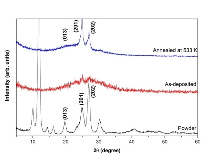 | Figure 1. XRD spectra of 3, 4, 9, 10-perylene-tetracarboxylicacid-diimide, PTCDI in powder form and thin film as indicated in the figure |
 ,
, ,
,  and
and . Table 1 gives the values of Miller indices hkl for each diffraction peak,
  and the interplanar spacing (
 ) before and after refinement. These patterns also indicate that the as-deposited film is amorphous/nanocrystalline structure, while the annealed film is crystallized with (201) and (202) orientations.
|
3.2. Optical characterizations
- The spectral behaviour of the transmittance, T and reflectance, R measured at normal incidence in a wavelength range 200–2500 nm for as-deposited and annealed PTDCI films of thickness 400 nm is shown in Fig. 2. It is quite clear that the intensities of transmittance within the absorption region increase by annealing process. Also, the maximum reflectance intensity for as-deposited film and annealing temperature show that the reflectance intensities within the absorption region. In transparent region, (
 ) all films have the same behaviour of T and R which indicate that the thickness does not change by annealing.
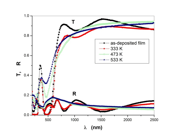 | Figure 2. The spectral dependence of the transmittance, T and reflectance, R for as-deposited and annealed PTCDI films with thickness of 400 nm |
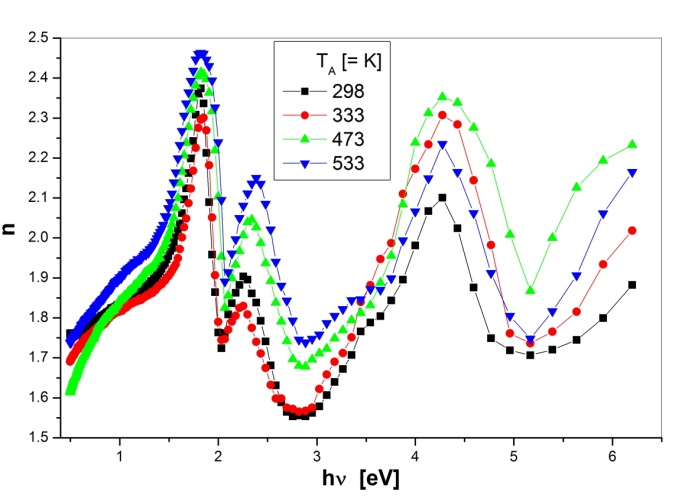 | Figure 3. Spectral dependence of the real part of refractive index, n, for as-deposited and annealed PTCDI films |
 ) and a normal dispersion in the range (
 ). At low photon energy,
  , the calculated value of real part of refractive index decreases by an amount of
  after annealing at 533 K. In addition (Fig. 3) shows three peaks at 1.8, 2.2 and 4.3 eV. There are visible variations in the intensity of these peaks with a blue shift in the peak positions as a result of annealing. It is also found that the films with lower refractive index correspond to higher annealing temperature, leads to a decrease in mass density[16]. Figure 4 shows the variation of the imaginary part of the refractive index, extinction coefficient, k with photon energy for as-deposited and annealed PTCDI films. There are considerable differences in the intensity and in the position of the absorption peaks for the as-deposited and annealed films. It is clear that, there is a blue shift in the absorption edge and the intensity of the absorption peaks decreases with annealing temperature.
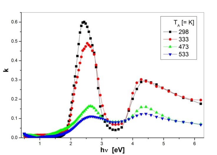 | Figure 4. Spectral dependence of the imaginary part of refractive index, k, for as-deposited and annealed PTCDI films |
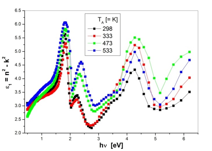 | Figure 5. The variation of real part of complex dielectric constant with photon energy for as-deposited and annealed PTCDI films |
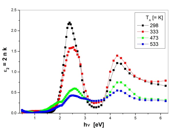 | Figure 6. The variation of imaginary part of complex dielectric constant with photon energy for as-deposited and annealed PTCDI films |
 characterizes completely the propagation, reflection and loss of light in thin film structure and provide important information about the electronic structure of materials. The complex dielectric constant is given by:
 | (4) |
 is the real part and
  is the imaginary part of the complex dielectric constant, while
  is the loss factor. Figures 5 and 6 show the real and imaginary parts of the complex dielectric constant, respectively. Hence, in the PTCDI films, the variation of
  as a function of photon energy follows the same behaviour as n, whereas the variation of
  follows the behaviour of k which is related to absorption coefficient
 .
.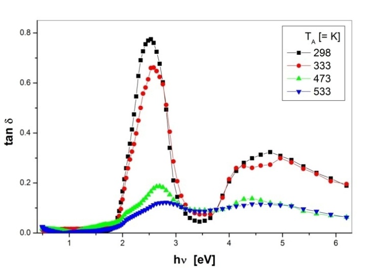 | Figure 7. The variation in the loss factor with photon energy for the as-deposited and annealed PTCDI films |
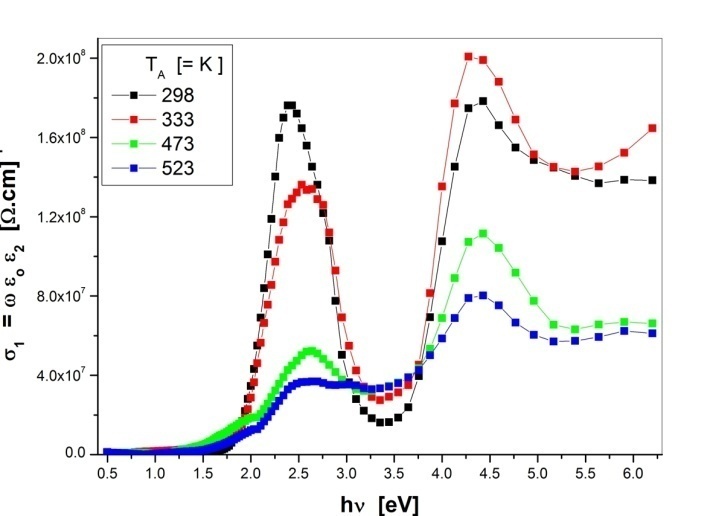
 with photon energy for the as-deposited and annealed PTCDI films is shown in Figure 7. The complex optical conductivity
  is related to the complex dielectric constant by the relation[17]:
 | (5) |
 is the permittivity of free space. The real
  and imaginary
  parts of the optical conductivity as a function of the photon energy are shown in Figures 8 and 9, respectively. It is also possible to calculate the volume and surface energy loss functions (VELF and SELF) by using the relations[18]:
 | (6) |
 | (7) |
 | (8) |
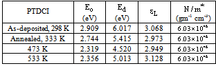
 is the single oscillator energy (is related to the lowest direct gap) and
  is the dispersion energy (is independent of both the absorption threshold (band gap) and the lattice constant)[20]. By plotting
  versus
  and fitting the data to a straight line,
  and
and  can be determined from the intercept,
  and the slope
 .
. | Figure 8. The variation of real part of optical conductivity with photon energy for as-deposited and annealed PTCDI films |
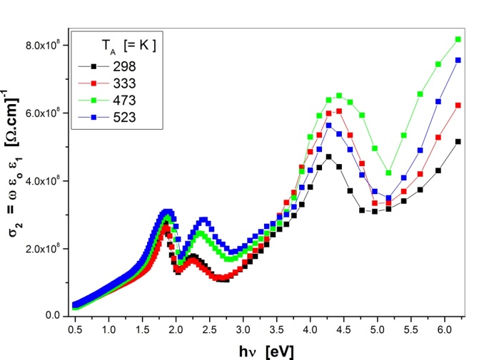 | Figure 9. The variation of imaginary part of optical conductivity with photon energy for as-deposited and annealed PTCDI films |
 | (9) |
 is the lattice dielectric constant, e is the elementary charge, c is speed of light and N/m* is the ratio of carrier concentration to the effective mass. The values of
  and (N/m*) are determined from the extrapolation of relation between n2 and
  to
to  and from the slope of the graph for the as-deposited and annealed PTDCI films and listed in Table 2.
 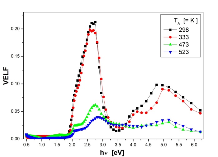 | Figure 10. VELF as a function of photon energy for as-deposited and annealed PTCDI films |
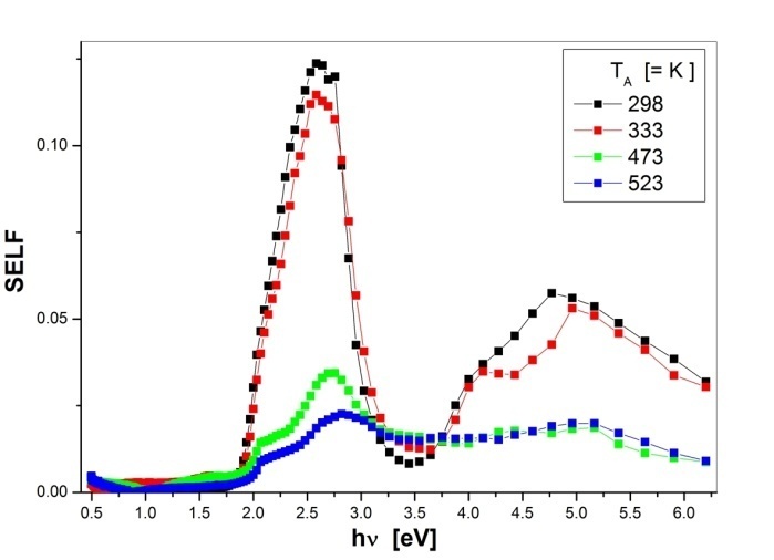 | Figure 11. SELF as a function of photon energy for as-deposited and annealed PTCDI films |
|
3.3. Optical Energy Gap
- The spectral distribution of the absorption coefficient (
 ) for as-deposited and annealed PTCDI films are shown in Fig. 12. The dependence of the absorption coefficient on the photon energy is important to obtain information about the energy band structure and the type of optical transition. The general expression that relates the absorption coefficient to the energy band near absorption edge is given by[24]:For allowed direct transitions
  | (10) |
 | (11) |
 and
and  represent the band gap energy, while
  and
and  are characteristic constant parameters, independent of photon energy, for direct and indirect transition, respectively.
 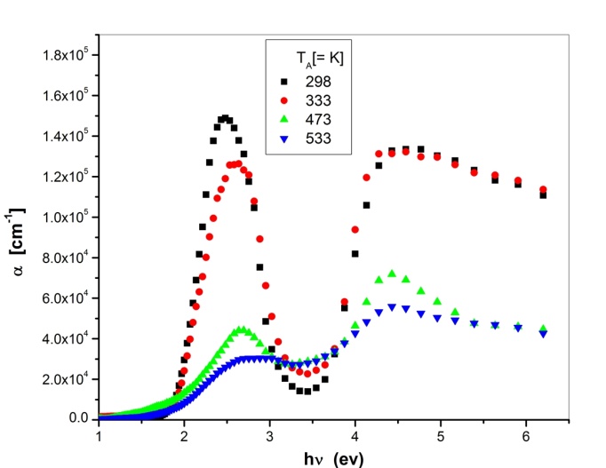 | Figure 12. Spectral behaviour of the absorption coefficient for the as-deposited and annealed PTCDI films |
|
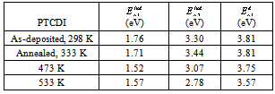
 versus
  (allowed direct transitions) and
  versus
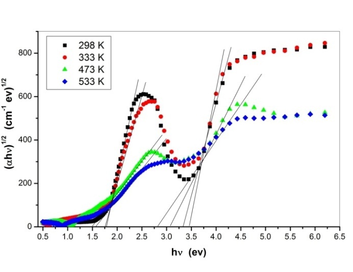
  (allowed indirect transitions) for the as-deposited and annealed PTDCI films are shown in Figs. 13 and 14 respectively. The extrapolation of the straight line graphs to zero absorption gives the values of the energy gap and these values are listed in Table 3. In case of indirect transition there are two different transitions. The value of the indirect energy gap decrease by increasing the annealing temperature. On the other hand, there is only one transition for direct type of transition. The values of direct energy gap also decreases by increasing the annealing temperatures. The decrease in the energy gap can be explained because of the thermal annealing results in more delocalized π electrons, the lowering of the band gap between π and π *, and the increase of the optical π - π * transition which results in the observed red shift in the gap[25,26].
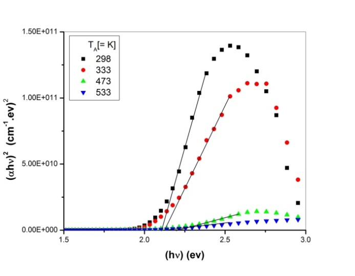 | Figure 13. The plot of  versus the incident photo energy ( versus the incident photo energy ( ) for as-deposited and annealed PTCDI films ) for as-deposited and annealed PTCDI films |
 | Figure 14. The plot of  versus the incident photo energy ( versus the incident photo energy ( ) for as-deposited and annealed PTCDI films ) for as-deposited and annealed PTCDI films |
4. Conclusions
- Effects of post-annealing on the optical characterization of thermally evaporated PTCDI films have been carried out using spectrophotometric measurements. It was found that the refractive index of the as-deposited film increases with annealing. In addition, annealing affects the values of calculated dispersion parameters. The optical absorption spectra of the PTCDI film shows that the absorption spectra mechanism is due to both direct and indirect transition. The decrease in the energy gap can be explained because of the thermal annealing results in more delocalized π electrons, the lowering of the band gap between π and π *, and the increase of the optical π - π * transition which results in the observed red shift in the gap. All the results are self-consistent in the paper. This work would benefit the fabrication and investigation of organic solar cell and photovoltaic devices.