-
Paper Information
- Next Paper
- Previous Paper
- Paper Submission
-
Journal Information
- About This Journal
- Editorial Board
- Current Issue
- Archive
- Author Guidelines
- Contact Us
American Journal of Materials Science
p-ISSN: 2162-9382 e-ISSN: 2162-8424
2012; 2(4): 125-130
doi: 10.5923/j.materials.20120204.05
Gaussian Distribution on Electrical Characteristics of Al/SiO2/p-Si Structures
 Abstract
 Reference
 Full-Text PDF
 Full-Text HTML
A. B. Selçuk 1, S. Bilge Ocak 2, S. Karadeniz 1
1Sarakoy Nuclear Research and Training Centre, 06983 Saray, Kazan, Ankara, Turkey
2Gazi University, Atatürk M.Y.O., Çubuk, Ankara
Correspondence to: S. Bilge Ocak , Gazi University, Atatürk M.Y.O., Çubuk, Ankara.
| Email: |  |
Copyright © 2012 Scientific & Academic Publishing. All Rights Reserved.
The Al/ /p-Si Schottky diodes (39 dots) with native interfacial insulator layer SiO2 were fabricated on the same Si wafer. The current-voltage (I-V) and capacitance-voltage (C-V) characteristics of metal-oxide-semiconductor diodes, which are based on Al/SiO2/p-Si structures, have been measured at room temperature. Barrier height (BH), ideality factor (n) of these diodes has been calculated from their experimental forward bias current-voltage (I-V), reverse bias capacitance-voltage. Even though they are identically performed on the same quarter Si wafer, the calculated values of BH, which is obtained from I-V characteristic, have ranged from 0.687 to 0.772 eV and ideality factor n from 1.903 to 4.48. The values of barrier heights obtained from C-V characteristics range from 0.629 to 1.097 eV. It was found that the values of barrier height  obtained C-V characteristics is larger than that of these values from I-V characteristics. The experimental values BH distribution obtained from I-V and C-2-V characteristics have been fitted by Gaussian function and their mean values of BHs have been calculated to be 0.730 and 0.863 respectively. Normal distribution of ideality factors mean value is 3.160 with standard deviation 0.689. Experimental results show that the interface states at a native insulator layer between metal and semiconductor play an important role in the value of the BH, ideality factor and the other electrical parameters of Schottky diodes.
Keywords: Schottky Diodes, MOS, Current-Voltage Characteristics, Capacitance-Voltage Characteristics, Gaussian Distribution
Article Outline
1. Introduction
- The electrical properties of metal-semiconductor (MS), metal-insulator-semiconductor (MIS) Schottky diodes have been investigated because of their importance in electronic device applications[1]. The mechanisms of carrier transport and some structural parameters of Schottky barrier diodes have been studied both experimentally and theoretically in past decades, but little experimental information are available on Schottky barrier formation and electronic states at metal-semiconductor (MS) interface[2]. It has been generally assumed that the thin insulating layers between the metal and semiconductor is uniform and has distinct effects on the behaviour of MS-diodes. In recent years, there are a vast number of reports on experimental studies of characteristic parameters such as the barrier height (BH) and ideality factor in MS or, metal-insulator-semiconductor (MIS) Schottky diodes and solar cells[3]. Also theoretical studies based on the effect of a Gaussian distribution of barrier height (BH) on I-V characteristics have also been reported in literature[4].The interface qualities between the deposited metal and the semiconductor surface determine the performance and reliability of Schottky diodes. Conduction mechanism of MS contact is mainly based on thermionic emission (TE) current model. It is well known that thin insulators between metal and semiconductor affect behavior of the Schottky diode characteristics. Existence of interfacial thin oxide layers between metal and semiconductor may change to electrical characteristics of Schottky diodes by interface state charges[5-7]. Thus, real characteristics of Schottky diodes are affected by interfacial oxide layers[7]. The behaviors of the I-V characteristics of Schottky diodes and MOS diodes describe these effects. Experimental studies of characteristic parameters such as the barrier height and ideality factor in MS and MOS diodes have been widely reported for decades. In addition, effects of Gaussian distribution of the barrier height (BH) and the ideality factors on I-V characteristics have been studied, too.In generally, the BH is likely to be a function of the interface atomic structure, and the inhomogeneity at a MS interface may be caused by grain boundaries, multiple phases, facets, defects, and a mixture of different phases[8,9]. Due to various reasons, calculation of barrier heights has a great importance to determine electrical characteristics in the semiconductor technology.The experimental effective BHs and ideality factors are obtained from I-V and C-V characteristics. These parameters are different from diode to diode even though they are identically prepared[10].In the present study, we have calculated barrier heights of MOS diodes from the experimental forward bias current-voltage and reverse bias capacitance-voltage characteristics of these diodes. Gaussian distribution of barrier height (BH) was obtained from C-2-V and I-V characteristics. Additionally, ideality factors were calculated from forward bias I-V and the Gaussian distribution of the experimental ideality factors has been acquired from I-V characteristics.
2. Experimental Procedure
- The semiconductor substrates were boron doped p-type Si single crystals with a (100) surface orientation, 280 µm thick and 1.1 Ωcm resistivity. As the first step, the Si wafer was degreased for 5 min in boiling trichloroethylene, acetone and ethanol respectively. RCA cleaning procedure was applied to the wafer in order to be chemically cleaned (i.e., a 10 min boil in NH3+H2O2+6H2O, followed by a 10 min boil in HCl+H2O2+6H2O), then immersed to diluted HF for 30 s, and finally bathed in deionized water of resistivity 18.3 MΩcm with ultrasonic vibration and dried by high-purity nitrogen. After surface cleaning, high-purity aluminium (Al) metal (99.999%) was thermally evaporated from the tungsten filament with a thickness of 1500 A onto the back surface of the wafer in vacuum about
 Torr. Then, temperature treatment at 500 oC for 3 min in N2 atmosphere was applied to a low-resistivity ohmic contact. The front surface of the Si wafer was exposed to air in a clean glass box for a month at room temperature to construct the native oxidation. The rectifying contacts were formed on the other faces by evaporating aluminum (Al, 99.999%) with a thickness of 1500 A˚ as dots with a diameter of about 1.0 mm through a metal mask at the pressure of
  Torr. Metal layer deposition rates were monitored with the help of a digital thickness monitor (FTM6). The deposition rates were about 10–20 s-1. Thirty nine dots (Schottky contact) on the same semiconductor surface were performed for the Al/SiO2/p-Si (MOS) Schottky barrier diodes. The I-V measurements were performed using a Keithley 2410 programmable constant current source. The C–V and conductance–voltage (G/ω-V) measurements were performed at various frequencies using an HP 4192A LF impedance analyzer at room temperature in dark at a test signal of 40 mVrms.
3. Results and Discussion
3.1. Current-voltage (I-V) characteristics
- The current through a Schottky barrier diode according to thermionic emission (TE) theory is given by the following relation[11-13]
 | (1) |
 | (2) |
 is reverse saturation current, q is the electron charge, V is the applied voltage, A is the effective diode area, A* is the effective Richardson constant which is 32 A cm-2K-2, T is the absolute temperature, R is the series resistance, n is the ideality factor and
  is the zero-bias barrier height. Ideality factor n can be obtained from Eq. (1) as
 | (3) |
 plot is the ideality factor, interception point of
  axis, which means zero applied voltage and gives us
  value in linear region above
  . Then, zero bias barrier height or apparent barrier height can be determined by using Eq. (3).
 | (4) |
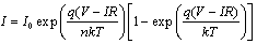
 , diodes are generally greater than unity caused by the effect of oxide layers, series resistances, inhomogeneities of barrier, etc[28]. One of the reason of barrier inhomogeneities in MOS structures may be attributed result of interface defects such as caused by grain boundaries, multiple phases, facets, defects, mixture of different phases, etc[29,30]. These effects cause for ideality factors to have larger values. Thus the inhomogeneities may play an important role and have to be considered in the evaluation of experimental I-V characteristics. As can be seen Fig.4, the BHs become smaller as the ideality factors increase. That is, there is a linear relationship between the experimental effective BHs and ideality factors of the Al/SiO2/p-Si SDs. The straight line in Fig.4 is the least squares fit to the experimental data. This finding may be attributed to lateral barrier inhomogeneities of Schottky diodes[16-27]. It has been mentioned that higher ideality factors among identically prepared diodes were often found to accompany lower observed BHs. The average BH value of approximately 0.775 eV for Al/SiO2/p-Si (MIS) diodes from extrapolation to n=1, will give the laterally homogeneous BH values. The difference between mean barrier height and lateral homogeneous barrier is the value of 0.045 eV. The value of the mean barrier height closes to lateral homogeneous barrier.
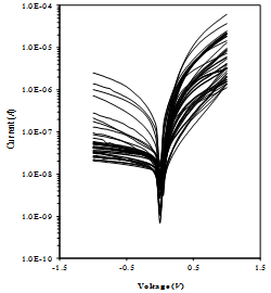 | Figure 1. Current-Voltage characteristics of Al/SiO2/p-Si MOS structure |
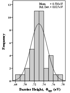 | Figure 2. Distribution of barrier heights obtained from I-V characteristics of MOS structures |
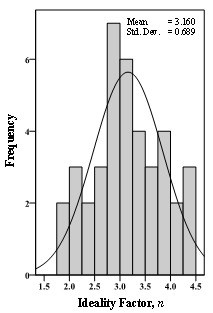 | Figure 3. Distribution of ideality factors obtained from I-V characteristics of MOS structures |
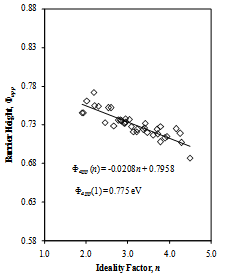 | Figure 4. Barrier height versus ideality factor plot of Al/SiO2/p-Si MOS structure |
3.2. Capacitance -voltage (I-V) characteristics
- Depletion layer capacitance of the diode is expressed as follow[7-9]
 | (5) |
 is the diffusion potential at zero bias which is determined from intersection point with V axis of C-2-V graphics,
  is the permittivity of semiconductor, A is the diode area, NA is the acceptor concentration of p-type Si semiconductor which can be obtained from slope of the C-2-V plot.Barrier heights from C-V characteristics are determined by
 | (6) |
 is the Fermi energy level,
  is the diffusion potential and
  is the image force barrier lowering.
  and
and  are given as
 | (7) |
 | (8) |
 is the effective density of states in Si valance band. This value for p-type Si substrate is 1.73×10¹⁶
 .Image force lowering can be expressed as
 | (9) |
 is the maximum electric field and is given by
 | (10) |
 with standard deviation of
  , respectively. Mean BH value with standard deviation and mean ideality factor with standard deviation are obtained from the statistical analysis of these parameters. The mean BH and a mean ideality factor values are 0.730 eV with standard deviation 0.017 eV and 3.160 with standard deviation 0.689, respectively. Ideality factor with greater than unity shows that there are series resistance of structure and localized interface states[31,32].The difference between the mean values of BHs obtained from C-V and I-V characteristics 0.133 eV is greater than the mean image force lowering value of 0.007 eV by using Eq. (9).As seen from the mean values, the difference between
  (I-V) and
  (C-V) for Al/SiO2/p-Si originates from the different nature of I-V and C-V measurements. Due to nature of the C-V ande I-V techniques barrier heights deduced from them are not always the same. The capacitance C is insensitive to potential fluctuations on a length scale of less than the space charge region and C-V method averages over the whole area and measures to describe BH. Additionally, the discrepancy between the devices may also be explained by the existence of an interfacial layer and trap states in semiconductor.As we know, the effective BHs and ideality factors from I-V and C-V measurements varied from each individual diode even which are prepared identically[10,18,25,26]. This result shows that the potential barrier at semiconductor interfaces depend more strongly on the applied voltage than predicted by the image-force effect for ideal contacts[17-19].
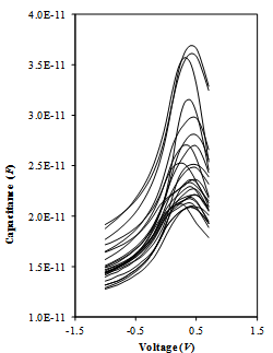 | Figure 5. Capacitance-Voltage characteristics of Al/SiO2/p-Si MOS structure |
 | Figure 6. C-2-V plot of Al/SiO2/p-Si MOS structure |
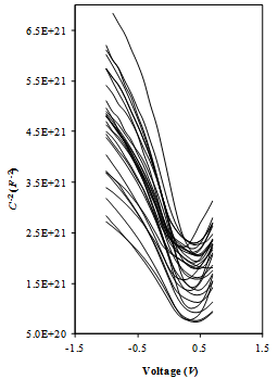
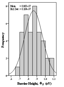 | Figure 7. Distribution of barrier heights obtained from C-V characteristics of MOS structures |
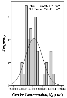 | Figure 8. Distribution of carrier concentrations of MOS structures |
4. Conclusions
- Electrical properties are measured from Al/SiO2/Si Schottky MOS diodes about 39 dots in this study. This structures prepared under the identical experimental conditions. Lateral homogeneous barrier height value is about 0.775 eV which is obtained from linear relationship between barrier heights and ideality factors. This value is lower than that of exact metal-semiconductor structure of Al/Si barrier height. Statistical analysis of barrier height and ideality factor from I-V measurements yields the mean effective barrier height as
 and ideality factor as
 . However, the mean barrier height from C-V measurement is
 . So, these values can be explained by oxide layer and lateral inhomogeneities.This study reveals that the effects such as interface states and insulator layer over I-V and C-V measurements must be taken into account. The main result of this work, although diodes were prepared as possible as identically, they have different characteristics from each other. This result shows that the potential barrier at semiconductor interfaces depend more strongly on the applied voltage than predicted by the image-force effect for ideal contacts[16,33]. Therefore, it is common practice to take averages for these values[18,33]. Statistical methods and computations can make more confidence results.