-
Paper Information
- Next Paper
- Previous Paper
- Paper Submission
-
Journal Information
- About This Journal
- Editorial Board
- Current Issue
- Archive
- Author Guidelines
- Contact Us
American Journal of Materials Science
p-ISSN: 2162-9382 e-ISSN: 2162-8424
2012; 2(3): 72-76
doi: 10.5923/j.materials.20120203.07
Electrical Characteristic Measurement of the Fabricated CdSe / P-Si Heterojunction Solar Cell Under Radiation Effect
 Abstract
 Reference
 Full-Text PDF
 Full-Text HTML
M. Ashry, S. Fares
National Center for Radiation Research and Technology (NCRRT), AEA, P.O. 29 Nasr City Egypt
Correspondence to: S. Fares, National Center for Radiation Research and Technology (NCRRT), AEA, P.O. 29 Nasr City Egypt.
| Email: |  |
Copyright © 2012 Scientific & Academic Publishing. All Rights Reserved.
The electrical and photovoltaic properties of CdSe/p-Si heterojunction solar cells prepared by evaporation cooting on a single-crystal p-type silicon substrates are examined ,under (100) mw/cm2, 25℃. The best fabricated cell shows an open-circuit voltage before irradiation is (0.62 V) and after irradiation is (0.44 V). The short-circuit current density before irradiation is (34 mA/cm2) and after irradiation is (13 mA/cm2). The fill factor before irradiation is (53 %) and after irradiation is (44.7 %). The conversion efficiency (active area) before irradiation is (11.1 %) and after irradiation is (2.5%). was observed during two-hour illumination test and after storing the cell in air for three months. The illumination is from the CdSe side (frontwall). The cells are analyzed using I-V and P-V measurements, spectral response and 1/C2-V measurements, with focus on the influence of the solar cell thickness, light intensity illumination and effective dose of γ-radiation, which play a crucial role to improve the solar cell efficiency. γ-irradiation campaign with different doses has been carried out on a series of solar cells.
Keywords: n-CdSe / P-Si Cells performance, γ-radiation Effects, Electrical and Photovoltaic Characteristics
Article Outline
1. Introduction
- The enormous gap between the potential of solar energy and our currently slight use of it is due to the modest energy density of the radiation, low conversion efficiencies of photovoltaic, and cost of materials currently required. The cost effective raising of conversion efficiency is primarily a scientific challenge: breakthroughs in fundamental understanding enable the development of materials and methods leading to the photovoltaic market progress. Several technologies have been developed for utilization of solar energy. Photovoltaic devices also known as solar cells convert solar energy to the electricity, which is the most convenient form of energy.Conventional single-junction semiconductor solar cells only effectively convert photons of energy close to the semiconductor band gap Eg as a result of the mismatch between the incident solar spectrum and the spectral absorption properties of the material[1]. Photons with energy Eph smaller than the band gap is not absorbed .Photons with energy Eph larger than the band gap is absorbed, but the excess energy Eph- Eg is not used effectively due to thermalization of the electrons. Several routes have been proposed to overcome these fundamental spectral losses that can account from as much as 50%. All these methods or concepts, which are referred to as Third Generation (3G) photovoltaic[2], concentrate on a better exploitation of the solar spectrum, e.g., intermediate band gaps[3], quantum dot concentrators[4] and down- and up-converters[5]. Third generation solar cells are the cutting edge of solar technology and still in the research phase. They are expected to achieve reasonable efficiencies at lower costs than first and second generation technologies[6] and contain a wide range of promising technologies including multijunction tandem cells [7], dye-sensitized solar cells (DSSCs)[8], organic solar cells based on small-molecule[9,10] and conjugated polymer [11,12], and organic/inorganic hybrid solar cells[13,14].The very first diffused silicon solar cells were made on n-type substrates in 1950s. The solar cell industry changed to p-type substrates soon after wards due to the higher resistance of this polarity to space radiation, when the only application for those cells was for space vehicles, and it is not be the best cell, choice for terrestrial application. N-type substrates usually have higher minority carrier life times than p-type substrates[15].There are four basic structures for the photovoltaic solar cells, homojunction, heterojunction p-i-n and n-i-p, multijunction.Heterojunction is a junction formed between two materials with different band gap[16,18]. A CdSe/p-Si solar cell involves a heterojunction formed between these two materials. Further, the semiconductor CdSe is used in heterojunction fabrication, as it has a good photosensitive and nano-crystalline property[19,20]. Sunlight is allowed to pass through the CdSe layer (band gap = 1.74 eV). In such a device the CdSe is referred to as the window layer. Cadmium solenoid has a nearly optimum band gap for the irradiation spectrum of sun light [21], thus the CdSe/p-Si thin film solar cell is promising candidate as a highly efficient and low-cost solar cell. However, to reduce the production cost and user hesitation due to toxicity of Cd, it is required to achieve a sufficient high energy conversation efficiency, using the PV active layer with a decreased thickness. On the other hand the PV performance of thickness solar cells is improved by the annealing temperature profile as will as the effect of γ-radiation.In this article, we report the results on structural and electrical and optical characterization of the (3, 7, 20 μm) thick CdSe/p-Si solar cells annealed under 525ok for 2 hours, dark (I-V) measurements and photo luminescence source used. In particular, we report the PV performances of (20 μm) thickness solar cell are improved by the modification of the thickness, effect of radiation and annealing temperature profile treatment .
2. Experimental Procedure
- the substrate materials are two-inch diameter (100) – oriented, p-type silicon wafers with a resistivity of (0.8-1.2 Ω.cm), corresponding with a doping density of (4-6)x1015 cm-3. These wafers were etched using CP4 etching solution for (2)min, (CP4 etching solution is prepared by adding 20mL of HF acid to 30 mL. Acetic acid and 60 mL concentrated HNO3). After etching, the Si-wafers were washed for 5 min. by distilled water, and then by ethyl alcohol. The CdSe: In film were evaporated onto the Si-wafers by using Cooting unit Edward type (E306A) , Evaporation was carried out at pressure (10-5 Torr ) in vacuum, to coated one side of the Si-wafers by n-CdSe thin film with different thickness. The CdSe thin film side, was over coated by an indium mesh to be used as grid electrode. After the CdSe: In film Coated, the ohmic rear contact was fabricated by vacuum evaporation of Gold, Indium silver, Bismuth and Aluminum electrodes. Then the front electrode was made by evaporating a Al metal grid, through a metal shadow mask. Finally, CdSe/p-Si Heterojunction were annealed for two hours (2H) at 523ok (250℃) to complete the Junction formation.
3. Results and Discussion
3.1. Electrical and Photovoltaic Characteristics of CdSe/ p-Si Solar Cell
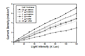
- The electrical characteristics of the photovoltaic cells were investigated in the dark and under different bias light conditions. The solar cell parameters, short circuit current density Isc, open circuit voltage Voc, and maximum out putted power (Pm) were determined. During dark I-V measurements, a light-proof cover shields the cell under test. The dark I-V curve is measured in forward and reverse directions as shown in Fig.(1) .For the measurements of the illuminated (I-V) curve a details investigation of solar cells, the illuminated (I-V) curves over a wide intensity range (10-120 k Lux).
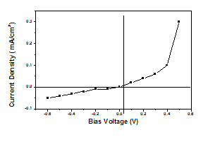 | Figure 1. Current voltage characteristics in dark |
|
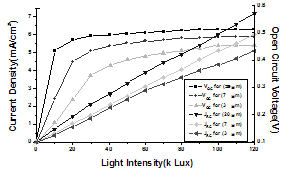 | Figure 2. Current density-voltage curve as a function of light intensity for different thickness cell |
3.2. Spectral Response Measurements
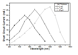
- Fig.(4) shows results of the spectral response for tested solar cells which were processed with different thickness (3, 7, 20 μm). As it can be seen, for whole cells, the optical properties of solar cells are almost the same trend but with different wavelengths range (i.e), as the solar cell thickness decrease, the maximum Isc value shifted towards the blue wavelength region.It can be noted that the spectral response at the long wave length decrease with the reduction in the (CdSe) layer thickness. Light transmission loss due to an insufficient absorption layer, and carrier recombination loss at the back contact , due to the probable presence of defect at the junction can be considered to be responsible for the total current loss in such thin films. In addition, the thin solar cell layer leads to the typically reduced response in the Infra Red region which leading to a significant reduction of recombination currents at the front surface .The spectral response behaviour can be discussed as follows, spectral down conversions was suggest in the 1970s to be used in so-called luminescent concentrators that were attached on to a solar cell [25]. In these concentrators, organic dye molecules absorb incident light and re-emit this at a red-shifted wavelength. Internal reflection ensures collection of all the re-emitted light in the underlying solar cells. As the spectral sensitivity of silicon is higher in the red than in the blue, an increase in solar cell efficiency was expected.
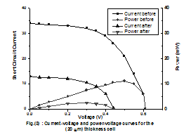 | Figure 3. current voltage and power voltage curves for the (20 μm) thickness cell |
 | Figure 4. Spectral response for different cell thickness |
3.3. Capacitance-Voltage Measurements
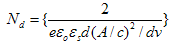
- One important property of semiconductor material is its charge carrier density. On the other hand, a too high carrier concentration causes unwanted recombination of the photogenerated charge carriers and thus deteriorates the conversion efficiency of the solar cell. Capacitance-voltage (C-V) measurements is the most commonly used method for the determination of carrier densities in semiconductor of material when the capacitance of a reverse biased semiconductor junction is measured as a function of the applied reverse bias (0.9 V), the apparent carrier density can be calculated from the slope of the (A/C)2 Vs.(V) plot according to the equation .
 Nd is the donor concentration in a p-type material, (e) is elemental charge, C is the space-charge capacitance, Vfb is the flat band potential, ε0 is the permittivity of free space, εs is the static permittivity of the semiconductor.Fig.(5) shows the 1/C2 –V plot of the CdSe/P-Si cell of Fig.(3) at (1 MHz) . Since band bending is primarily on the CdSe-Side, the (1/C2 –V) intercept of (0.9 V) on the x-axis is essentially equal to the diffusion potential within the CdSe. The slope of the straight line gives donor concentration Nd of ( ≈ 4.6x 10¹⁵) cm-3 .The C–V characteristics of CdSe / P-Si heterojunction was measured by applying reverse biased potential. When heterojunction was just irradiated with gamma irradiation the slope of the plot was found to be decreased. This is attributed to the increase in capacitance due to increase in charge carriers across the junction where electrons are drifted in n-region and holes are drifted in p-region. The extrapolated plots intersect on bias voltage axis at 0.9 V giving the value of built-in junction potential to be 0.9 eV. The crossover of the extrapolated plot on voltage axis shows the formation of abrupt p–n, (p)Si-/(n)CdSe, junction. But the increase is equal in magnitude for both types of charges; hence, essentially built-in junction potential has not changed. This also show that there are no structural changes or diffusion across the junction due to laser irradiation
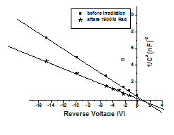 | Figure 5. The (1/C2-V) of the C dSe/p-Si solar cell at frequency of (1MHz) |
3.4. Effect of γ-radiation on Solar Cell Performance
- We have performed γ-exposures to study performance reliability and materials degradation of our fabricated solar cell. All the cells with different thickness was irradiated by γ-radiation with different doses (500, 1400, 1900 M Rad).In general, effects can be produced at the surface or in the bulk. Surface effects will clearly be most important for thin films[26], have suggested that the break point for considering only surface damage comes for thickness less than ( ~ 20 μm), and that in this case it is the energy fluency which is important (propagation of defects out of the irradiation layers take place over distance of 1-10 μm). For thicker materials both surface and bulk effects have to be considered, (i.e) the main effects are due to total ionizing dose[27,29]. They occur at higher levels than generally encountered in the natural space environment. For the three type solar cells with different thickness (0.3, 7, 20 μm), Fig.(6) shows that thin film solar cells have excellent radiation hardness . The results show that the thinner cells are only very slightly damaged than the more thickness ones (20 μm) which has the great degradation by γ-irradiation at a chosen fluency (1900 M Rad) .The photoelectrical characteristics (J–V curve) for the different cells thickness (3,7,20) were measured before and after γ-irradiation. The measured short circuit current density, open circuit voltage, fill factor and efficiency are 34 mA/cm2, 0.62 V, 52.6% and 11.1% for cell (20 μm) Fig. (3) For cell (3 μm) are 28 mA/cm2, 0.49 V, 34% and 4.8%. While the photoelectric performance before irradiation is better in cell (20 μm) compared with the corresponding one in cell (3 μm), due to the better spectral response for cell (20 μm) than in cell (3 μm), as shown in Table. (1). Also the strong effect of γ-radiation on the short circuit current (Jsc) and the open circuit voltage (Voc) is clearly observed. This is attributed to the permanent crystal damage created in the base region reducing the electronic lifetime of the generated carriers.During crystal damage, three phenomena, namely generation of electron–hole pairs, Compton effect and electron–positron pairs, occurred [30]. It is also observed that the gamma rays have a greater effect in reducing the Jsc than in Voc for cell (20 μm). The degradation percentage ratios in Jsc and Voc are 38% and 70 % for (20 μm) and 82% and 70% for cell (3 μm), respectively.
 | Figure 6. The effect of gamma radiation (1900 M Rad) on current density for different cell thickness |
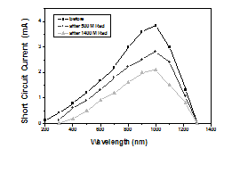 | Figure 7. Spectral response of (20 μm) cell thickness as a function of gamma dose |
4. Conclusions
- The fabrication of CdSe/p-Si Heterojunction by physical thermal evaporation method has been reported .We have investigated the influences of various conditions in the CdSe/p-Si solar cell performance. The effect of cell thickness were observed. The thin CdSe/p-Si cell .thickness leads to the typically reduced spectral response in the infrared, and the wave length which has the maximum spectral response was shifted towards the shorter wave length, as the cell thickness decrease .In addion the radiation hardness of solar cell performance. The effect of cell thickness was observed. The thin CdSe/p-Si solar cell was studied for γ- doses (500, 1400 Mrad). The effects of radiation noted a decrease in electrical performance as the radiation dose increase. Parameters such as donor concentration in CdSe, as well as current – voltage, and capacity voltage is described. Efficiency of the best performance solar cell CdSe/ Si approached around 11 %.