-
Paper Information
- Next Paper
- Previous Paper
- Paper Submission
-
Journal Information
- About This Journal
- Editorial Board
- Current Issue
- Archive
- Author Guidelines
- Contact Us
American Journal of Materials Science
p-ISSN: 2162-9382 e-ISSN: 2162-8424
2012; 2(2): 6-10
doi: 10.5923/j.materials.20120202.02
Photoluminescence Studies on Nanocrystalline Tin Oxide Powder for Optoelectronic Devices
L. C. Nehru 1, V. Swaminathan 2, C. Sanjeeviraja 1
1School of Physics, Alagappa University, Karaikudi, 630002, India
2School of Materials Science and Engineering, Nanyang Technological University
Correspondence to: C. Sanjeeviraja , School of Physics, Alagappa University, Karaikudi, 630002, India.
| Email: |  |
Copyright © 2012 Scientific & Academic Publishing. All Rights Reserved.
Nanocrystalline tin oxide (SnO2) powders have been synthesized by a low temperature chemical precipitation method. As-prepared and heated powders were characterized by XRD, SEM and luminescence studies. Crystallographic parameters such as crystallite size, lattice parameters and dislocation density in SnO2 nanocrystalline powders were calculated by Rietveld analysis. The average crystallite size of 9 - 43 nm was obtained for SnO2 powders through controlled heat treatment process. The washed powders morphology was almost spherical in shape and average agglomerate crystal size was between 0.2 – 0.4 μm. A Photoluminescence (PL) study was measured at an excitation wavelength of 265 nm for as-prepared and annealed powders; it showed a broad emission peak at 417 nm for all powders. The highest PL emission was attained for the powder annealed at 500℃. The synthesized nanocrystalline SnO2 oxide semiconductor material could be suitable for making optoelectronic and sensor devices.
Keywords: Nano, SnO2, Oxide, Chemical precipitation, Photoluminescence
Article Outline
1. Introduction
- Over recent years, nanoscience and nanotechnology are attracting and focusing more attention in many commercial applications. In semiconductor nanoparticles, particle size, shape and surface states are the predominant factors, which influences its properties such as optical, magnetic, electric and catalytic[1]. The optical properties with size effect of nanocrystalline semiconductors have been a subject of great interest in recent years. In quantum size effect, when the particle size of a semiconductor is compared to the Bohr radius[2], the ratio of surface atoms to those with the interior enhances the surface properties of the material. Due to these effects, band gap of the semiconductor nanoparticles has been modified, which makes a lot of changes in their electronic properties when compared to the bulk. Thus, there is an increase in the band gap i.e. the visible spectra show a blue shift, which is ascribed to quantum size effect[3]. This stimulated a great interest in both basic and applied research in semiconductor oxide nanomaterials. Recently tremendous R&D efforts in materials with reduced dimensions, in nanometer scale, have been developed for the fabrication of new miniaturized electronic devices and sensors, which would work more efficiently and selectively as compared to the existing devices so far. Among the various semiconductor materials, conducting n-type semiconductor tin oxide (SnO2) is having a wide band gap of Eg = 3.6- 3.8 eV [4] at room temperature. This conducting oxide is a well known functional material, which can be operative at low temperature with high sensitivity for applications such as gas sensors, transparent conducting electrode, transistor, solar cells, special coating for energy-conversion, low-emissivity windows, and nanoelectronic devices[5-7]. Thus, a great deal of research work has been devoted to the method of synthesizing SnO2 particles of nano sizes in a controllable manner.Many efforts have been applied to synthesize the SnO2 nanoparticles and nanowhiskers[8] and several methods have been developed for the synthesis of SnO2 nanoparticles like sol-gel route, chemical vapor deposition, thermal decomposition[9], co-precipitation[10], microwave-assisted solution[11], gas phase condensation[12] and laser ablation[13] etc., Preparation of nano-particles of SnO2 at low cost in industrial scale is a challenge in material production. So, using the cheap materials, simple synthesize route and suitable conditions of synthesis are the main requirement for this process. Therefore, the study of influence of various process parameters such as initial solution combination, time and temperature of heat treatments is very important for nanopowder production. The main purpose of the present research is to study the post-annealing temperature effect on nanoparticles size of SnO2 powders synthesized by the low temperature chemical precipitation method. A few publications described the production of SnO2 nanopowders by chemical synthesis. However, it is a challenge to find an efficient and simpler way, using low temperature, cost effective, homogeneous and convenient method suitable for large scale production of SnO2 powder with particle size about several nanometers by using this method. However, earlier research of high surface area powders with agglomeration and irregular particle morphology of tin oxide powders were reported. In the present context, it is challenging to overcome the above drawbacks through a controlled chemical precipitation method. Zhijie Li[7] recently reported the room temperature photoluminescence of blue emission with weak intensity. Few reports have been published on the luminescent characteristic of SnO2 nanocrystalline powder by chemical methods. Particle size plays a significant role in optical properties and its emission shift occurs due to the recombination of the electrons with holes in the valence band. Hence, it is another challenge to produce nanomaterials with stronger luminescence property with peak shift. In order to overcome the above drawbacks, we produced SnO2 nanocrystalline powders with desire size by chemical precipitation method which could enhance the photoluminescence property of the material. In the present paper, a systematic study on nanocrystalline SnO2 powder of various sizes by a simple low temperature chemical synthesize route, which can be subsequently processed by different annealing temperature has been presented in detail. Characterization of crystallographic parameters and photoluminescence shift for different annealing temperatures were performed and the results are discussed.
2. Experimental
- The experimental steps involved in the preparation of SnO2 nanocrystalline powder is shown in Fig.1.
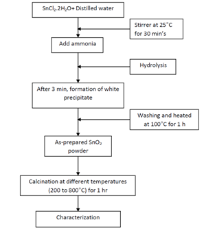 | Figure 1. schematic representation of nanocrystalline sno2 powders by chemical precipitate method |
2.1. Characterization
- The as-prepared and annealed nanocrystalline SnO2 powder was characterized by powder X-ray diffraction (XRD) method using a X’Pert PRO PANalytical diffractometer with CuKα radiation of wavelength 1.5405 Å. Diffraction patterns were recorded with a step size of 0.02°, scan speed of 2 s/step and scan angle 2θ from 10° to 80°. Crystallographic parameters were refined by XRD pattern and Rietveld refinement using TOPAS-3 and Diamond software was used to construct the structural parameters. The dislocation density (δ), defined as the length of dislocation-lines per unit volume of the crystal can be calculated from d = 1/D2 [14], where D is the crystallite size and the number of unit cell is calculated from n = 3.14 x (4/3) x (D/2)3 x (1/V) [15], where D is the crystallite size and V is the cell volume of the SnO2 sample. Morphological of as-prepared and annealed samples was examined by SEM (JEOL-6360). Nanoparticles and diffracted rings pattern was obtained from JEOL 2010 Transmission Electron Microscope. The photoluminescence measurements were carried out from 280 nm to 480 nm at room temperature using Varian Cary Eclipse spectrophotometer with 265 nm as the excitation wavelength of a 15 W Xenon pulse lamp. All emission spectra were recorded for the detector response and excitation spectra for the lamp profile.
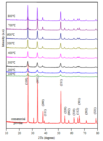 | Figure 2. The XRD patterns of SnO2 samples before and after annealed at different temperatures from 200 to 800℃ and peaks were indexed to the bulk SnO2 (MERCK) with JCPDS no. 88–0287 |
3. Results and Discussion
- Figure 2 shows the XRD patterns of SnO2 nanocrystalline powders for as –prepared and annealed powders at different temperatures from 200 to 800℃. For as-prepared and annealed powders, the XRD data showed that the tetragonal SnO2 phase was successfully produced, its lattice parameters were a =4.7493 nm and c =3.1898 nm (as-prepared); the lattice constants were comparable with earlier reports.
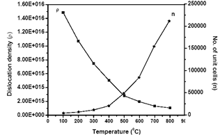 | Figure 3. Variation of Dislocation density and number of unit cells as a function of temperature |
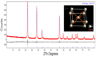 | Figure 4. Rietveld refinement of nanocrystalline SnO2 powder annealed at 500℃ for 1 h |
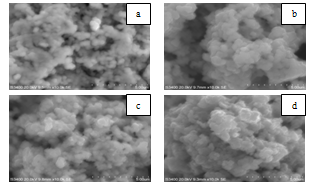 | Figure 5. Scanning electron micrographs of nanocrystalline SnO2 samples at different annealed temperatures (a) as-prepared, (b) 200℃, (c) 500℃ and (d) 800℃ |
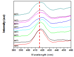 | Figure 6. Photoluminescence emission spectra of SnO2 heated at different temperatures (λex=265 nm) |
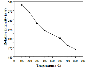 | Figure 7. Temperature dependence of relative photoluminescence intensity at 417 nm |
5. Conclusions
- In summary, tin oxide (SnO2) nanocrystalline powders are successfully synthesized by a simple precipitation method obtained at 100°C by a reaction of SnCl2 and NH3. The XRD patterns confirmed that SnO2 nanocrystalline powders possess a tetragonal rutile structure. The average crystallite size of the nanopowders are in the nanometer range, upon increasing the temperatures the crystallite size of the SnO2 was found to increase from 9 to 43 nm. The heating effect has influence the size of the crystallite on the nanocrystal powders. When samples were heated, the lattice parameters and dislocation density were decreased, so a smaller number of unit cells start to grow. Then, the obtained Rietveld refinement index value with weight percentage is ~11%, R Bragg value is ~1% and good of fitness is ~1% having good agreement in earlier reports. Photoluminescence emission exhibits a band at 417 nm. It is related to the recombination of electrons in singly occupied oxygen vacancies with photoexcited holes in the valence band. Then the heating temperature can also affect the luminescence process, the emission resulting in the decrease in the oxygen vacancies, as revealed by the decrease in luminescence at 417 nm.
ACKNOWLEDGEMENTS
- One of the authors, L.C.Nehru would like to thank University Grants Commission (UGC), India for the financial support under Research Fellowship in Sciences to Meritorious Students (RFSMS) to carry out this research work at School of Physics, Alagappa University, Karaikudi-3, India.
 Abstract
 Reference
 Full-Text PDF
 Full-Text HTML